N A N O E X P R E S S
Open Access
Low Power Consumption
Substrate-Emitting DFB Quantum Cascade Lasers
Chuan-Wei Liu
1,2, Jin-Chuan Zhang
1*, Zhi-Wei Jia
1,2, Ning Zhuo
1, Shen-Qiang Zhai
1, Li-Jun Wang
1,2, Jun-Qi Liu
1,2,
Shu-Man Liu
1,2, Feng-Qi Liu
1,2and Zhan-Guo Wang
1,2Abstract
In the present work, an ultra-low power consumption substrate-emitting distributed feedback (DFB) quantum cascade laser (QCL) was developed. The continuous-wave (CW) threshold power dissipation is reduced to 0.43 W at 25 °C by shortening the cavity length to 0.5 mm and depositing high-reflectivity (HR) coating on both facets. As far as we know, this is the recorded threshold power dissipation of QCLs in the same conditions. Single-mode emission was achieved by employing a buried second-order grating. Mode-hop free emission can be observed within a wide temperature range from 15 to 105 °C in CW mode. The divergence angles are 22.5oand 1.94oin the ridge-width direction and cavity-length direction, respectively. The maximum optical power in CW operation was 2.4 mW at 25 °C, which is sufficient to spectroscopy applications.
Keywords:Quantum cascade laser, Substrate-emitting, Low power consumption
Background
In recent years, quantum cascade lasers (QCLs) have undergone a rapid development and become the most promising source in the mid-infrared frequency region [1–3]. Benefited from their high power, single-mode operation and compact size, distributed-feedback (DFB) QCLs have been widely used in many applications such as trace-gas sensing, free space communication, and substance analysis [4–6]. However, the remaining dis-advantage of QCLs is their high electrical power dissi-pation, which has limited their application in some portable and highly integrated systems. To decrease the power dissipation, the most straightforward method is to decrease the geometry size of the device, such as shortening the cavity and narrowing the ridge. High-re-flectivity (HR) coating is also very effective for reducing the mirror loss. Some studies have been done to reduce the threshold power dissipation of Fabry-Perot (FP) QCLs by using a short cavity and depositing HR coating [7] or partial high-reflectivity (PHR) coating on the
facets [8], in which the dissipated power as low as 1.2 W at 22 °C and 0.83 W at 25 °C have been demonstrated by A. C. Richard et al. and Y. Bai et al., respectively. These methods could also be applied to DFB devices. In 2014, Ryan M. Briggs et al. reported a single-mode DFB QCL emitting at 4.8 μm with a CW threshold power con-sumption of 0.76 W and maximum optical power of about 17 mW at 20 °C [9]. In 2015, A. Bismuto et al. demonstrated short cavity, narrow ridge single-mode DFB QCLs emitting at 4.5μm with CW threshold dissi-pated power as low as 0.5 W at 20 °C [10]. The max-imum optical power is about 150 mW; however, the injected electrical power is more than 6 W. Other methods such as doping optimization and low-period active structure have also been investigated [7, 11]. For edge-emitting QCLs, HR coating is commonly deposited on the back facet and leaving the front facet uncoated or PHR coated to reduce mirror loss meanwhile maintain-ing the optical power emitted from the front facet. Instead, both facets can be HR coated for substrate-emitting to further decrease the mirror loss since the light is emitted from substrate instead of front facet. Be-sides, improved far-field distributions can be expected from substrate-emitting QCLs [12, 13]. According to our recent work, a substrate-emitting DFB QCL with low threshold power dissipation of 1.27 W at 20 °C * Correspondence:[email protected]
1Key Laboratory of Semiconductor Materials Science, Institute of
Semiconductors, Chinese Academy of Sciences, Beijing Key Laboratory of Low Dimensional Semiconductor Materials and Devices, Beijing 100083, People’s Republic of China
Full list of author information is available at the end of the article
was obtained by depositing HR coating on both facets [14]. The active region in Ref [14] consists of 40 super-lattice periods, and the threshold voltage is about 13 V. A lower threshold voltage, and thus, lower threshold power dissipation can be expected if the period number of active region is decreased. The cavity length of 1 mm could also be further shortened by properly designing the buried second-order grating to decrease the threshold power dissipation.
In the present work, an ultra-low power consumption substrate-emitting DFB QCL was developed. The thresh-old power dissipation working in CW mode is as low as 0.4 W at 15 °C and 0.43 W at 25 °C by shortening the cavity length to 0.5 mm and depositing HR coating on both facets. The maximum optical power in CW mode is 2.4 mW at 25 °C, which is sufficient to spectroscopy applications. Single-mode emission was achieved by employing a buried second-order grating. The divergence angles are 22.5o and 1.94o full width at half maximum (FWHM) in the ridge-width direction and cavity-length direction, respectively. The double-lobed far-field distri-bution in cavity-length direction indicates that anti-symmetric mode is favored. These devices can operate in CW mode without mode-hop in a wide temperature range from 15 to 105 °C and will be very suitable in high-integrated portable applications.
Methods
The active region of the device was based on strain-compensated two-phonon resonant design emitting at ~ 4.6 μm. The wafer was grown on an n-doped (Si, 2 × 1017 cm−3) InP substrate by solid-source molecular beam epitaxy (MBE). Thirty stages of In0.67Ga0.33As/
In0.36Al0.64As quantum wells and barriers were included
in the active core, which was similar to Ref. [15] The entire layer sequence was as follows: 1.2-μm-thick lower cladding layer (Si, 2.2 × 1016 cm−3), 0.3-μm-thick n-In0.53Ga0.47As layer (Si, 4 × 1016 cm−3), 30
active/in-jector stages, 0.3-μm-thick n-In0.53Ga0.47As layer (Si,
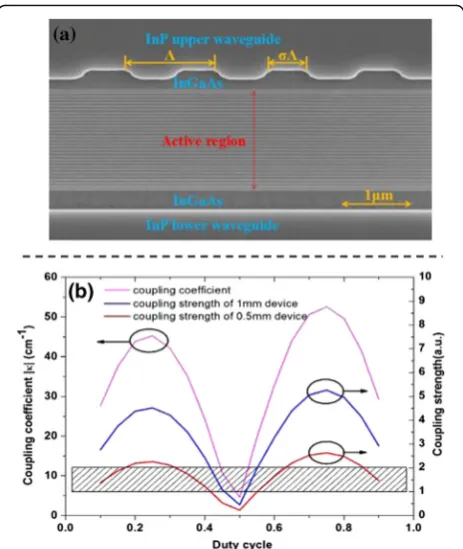
4 × 1016 cm−3), and top waveguide cladding player. To fabricate the buried grating, the top waveguide cladding layer was removed down to the upper InGaAs layer. The second-order grating with a period ofΛ= 1.42μm (duty cycle σ = 0.45, depth d = 130 nm) was defined on the 0.3-μm-thick upper InGaAs layer by holographic lithog-raphy technology and wet chemical etching. Figure 1a shows the scanning electron microscope (SEM) image of the buried second-order grating. After that, a 3-μ m-thick low-doped InP layer (Si, 2.2 × 1016cm−3) followed by a 0.15 μm gradually doped InP layer (Si, from 1 × 10¹⁷to 3 × 1017cm−3) and a 0.4-μm high-doped InP cladding layer (Si, 5 × 1018cm−3) were accomplished in sequence as upper cladding by metal-organic vapor phase epitaxy (MOVPE).
Following the implementation of the regrowth, the wafer was etched into double-channel waveguide struc-ture with an average core width of 7 μm. Then, a 450-nm-thick SiO2 was deposited by plasma-enhanced
chemical vapor deposition (PECVD) for insulation. A
2-μm-wide electron injection window was patterned on SiO2 layer of the ridge, and electrical contact was
pro-vided by a Ti/Au layer. For better heat dissipation, an additional 4-μm-thick Au layer was electroplated. Before actually cleaving, massive simulations for the design of the second-order buried grating was implemented with finite element method software (COMSOL), which was similar to Ref. [16] After thinning to 150μm, the wave-guide was cleaved to 0.5- and 1-mm-long devices, corresponding to coupling strength of 0.54 ~ 1.77 and 1.08 ~ 3.55, respectively. Then, both facets of these de-vices were HR coated by e-beam evaporation. The HR coating consisted of Al2O3/Ti/Au/Al2O3 (200/10/100/
120). The devices were mounted epi-layer down on copper heat sinks with indium solder, and then, wire bonded to an external contact pad.
Device testing was done on a thermo-electric cooler (TEC) stage with a thermistor regulating and monitoring the temperature of the heat sink. The output power of the QCL was measured by a calibrated thermopile de-tector (Coherent, EMP1000) that was put right in front
[image:2.595.306.538.86.361.2]of the device with a metallic tube collecting the laser emission. Then, the device was put on a step-motor con-trolled rotational stage with a resolution of 0.01ofor far-field distribution test and a room temperature HgCdTe detector (Vigo, PVMI-10.6) was put in front of the laser with a distance of 30 cm to detect the radiation. The spectra measurement was carried out using a Fourier transform infrared (FTIR) spectrometer (Thermo Fisher Scientific, Nicolet 8700) with a resolution of 0.25 cm−1 in rapid scan mode.
Results and Discussion
The COMSOL simulation result is shown as Fig. 1b. Ac-cording to the calculation, a coupling coefficient of |κ| = 35.5 ~ 10.75 cm−1is obtain for the buried grating with duty cycle of 0.35 ~ 0.45 and etching depth of 180 nm. The coupling strength g= |κ|L, whereL is the cavity length of the QCL. To obtain efficient surface emission, the coupling strength of 1–2 is always re-quired. For a device with 1 and 0.5 mm cavity-length, the simulated coupling strength are in the range of 3.55 ~ 1.07 and 1.78 ~ 0.54 when the duty cycle is 0.35 ~ 0.45. Therefore, the design of the buried grating is very essential for short cavity-length device.
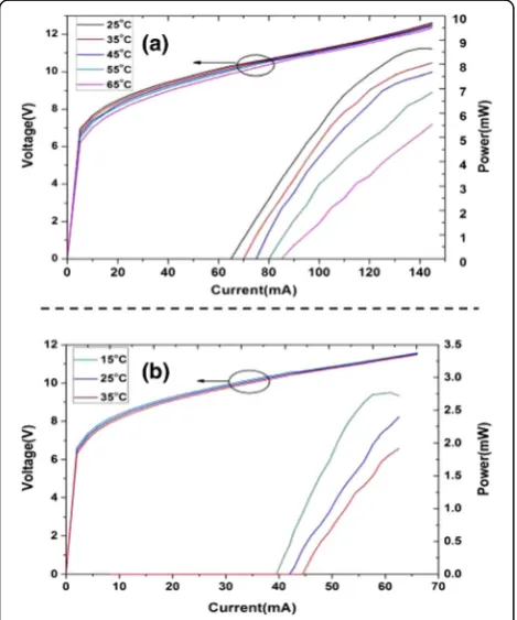
Of particular interest is the electrical characterization. The light-current-voltage (L-I-V) curve of the devices with different cavity length is shown as Fig. 2. The lasers
operated in CW mode and the heat sink temperature was regulated by a temperature controller (Thorlabs, ITC-QCL-4000). As shown in Fig. 2a, the device with 1 mm-long cavity exhibits a threshold current of 65 mA at 25 °C, corresponding to a threshold current density of 0.54 kA/cm−2 and power dissipation of 0.67 W. The maximum optical power is 8.6 mW with an injected electrical power of 1.66 W, and the slope efficiency is 0.11 W/A. At high temperature of 65 °C, the maximum optical power is still more than 5 mW. For a 0.5 mm cavity-length device, the threshold current and power dissipation are decreased to 39 mA and 0.4 W at 15 °C, as shown in Fig. 2b. The threshold current density is 0.65 kA/cm−2. The maximum optical power of 2.8 mW is deduced when the injected electrical power is 0.74 W. At 25 °C, the threshold current is slightly increased to 41 mA, corresponding to a power consumption of 0.43 W. As far as we know, this is the lowest threshold power consumption of QCLs at the same temperature. The maximum optical power of this device is 2.4 mW with a power dissipation of 0.76 W, which is very capable of some high-integrated sensor applications. At 35 °C, the maximum optical power is about 1.9 mW. This device can operate at temperature as high as 105 °C in CW
Fig. 2The L-I-V characteristics of the 1 mm (a) and 0.5 mm (b) devices
[image:3.595.307.540.395.707.2] [image:3.595.57.292.423.705.2]mode, but the output power will become small and too difficult to detect accurately. Compared to the previous works in Ref [9–11], the maximum optical power of our design is not remarkable because of the low wall-plug ef-ficiency of the device. This is inherently limited by the quality of the epitaxy wafer. Besides, the maximum wall plug efficiency of 0.5 mm cavity-length device is 0.32% at room temperature, less than that of 1 mm cavity-length device, i.e., 0.5%.
[image:4.595.58.291.391.692.2]The spectra characterization of the lasers is shown in Fig. 3. Both of the 1 and 0.5 mm devices can operate in CW mode without mode hop within a wide temperature range from 15 to 105 °C. This is the highest working temperature in all of the low power consumption QCLs. Such a high working temperature is mainly benefited from the reduced mirror loss brought by the HR coating on the facets. The temperature shift coefficient is − 0.21 cm−1/K and−0.19 cm−1/K, respectively. There is a small difference between the spectra regimes of the two devices at the same temperature range, which is prob-ably caused by the nonuniform lithography and etching process of the grating. The side-mode suppressing ratio (SMSR) of device is about 25 dB. The good linear tuning capability, single-mode and high operating temperature
of these devices make them very useful in some real ap-plications such as trace gas sensing.
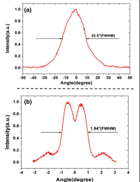
The far-field distribution of a 0.5 mm device is shown in Fig. 4. In ridge-width direction, a single-lobed pattern with divergence angle of 22.5o (FWHM) is observed, as shown in Fig. 4a. Figure 4b shows the far-field pattern in the cavity-length direction. The far-field pattern indicates that anti-symmetric mode is favored, which is caused by the nonuniformities of handmade cleaving and residual facet reflections [16]. Symmetric mode can be obtained by the use of distributed Bragg reflector (DBR) grating on both side of the DFB grat-ing region to eliminate the uncontrolled cleaved facets reflections [17].
Conclusions
We have developed a substrate-emitting DFB QCL with an ultra-low threshold power dissipation of 0.43 W at 25 °C operating in CW mode by shortening the cavity length to 0.5 mm and depositing HR coating on both of the facets. Its maximum optical power was 2.4 mW, and the corresponding power dissipation was 0.76 W. Single-mode emission without Single-mode-hop was obtained within a wide temperature from 15 to 105 °C by defining a buried second-order DFB grating. The divergence angles are 22.5o and 1.94oin the ridge-width direction and cavity-length direction, respectively. The low-consumption characteristic of the device could make it a promising light source in some battery-powered portable systems.
Abbreviations
CW:Continuous wave; DFB: Distributed feedback; FP: Fabry-Perot; FTIR: Fourier-transform infrared; FWHM: Full width at half maximum; HR: High reflectivity; MBE: Molecular beam epitaxy; MOVPE: Metal-organic vapor phase epitaxy; PECVD: Plasma-enhanced chemical vapor deposition; PHR: Partial high reflectivity; QCL: Quantum cascade laser; SEM: Scanning electron microscope; SMSR: Side-mode suppressing ratio; TEC: Thermo-electric cooler
Acknowledgements
This work was supported by the National Basic Research Program of China (grant no. 2013CB632801), National Key Research and Development Program (grant no. 2016YFB0402303), National Natural Science Foundation of China (grant nos. 61435014, 61627822, 61574136, 61404131, and 61674144), Key Projects of Chinese Academy of Sciences (grant nos. ZDRW-XH-2016-4 and QYZDJ-SSW-JSC027), and Beijing Natural Science Foundation (grant nos. 4162060 and 4172060).
We thank Ping Liang and Ying Hu for their help in device processing.
Authors’Contributions
CWL fabricated the device, performed the testing, and wrote the paper. JCZ and FQL designed the structure, provided the concept, and supervised the project. ZWJ, JQL, LJW, and SML supervised the testing. NZ and SQZ completed the MBE growth. ZGW supervised the project. All authors read and approved the final manuscript.
Competing Interests
The authors declare that they have no competing interests.
Publisher’s Note
Springer Nature remains neutral with regard to jurisdictional claims in published maps and institutional affiliations.
Fig. 4The far-field distribution of a 0.5-mm cavity-length device.a,
Author details
1Key Laboratory of Semiconductor Materials Science, Institute of
Semiconductors, Chinese Academy of Sciences, Beijing Key Laboratory of Low Dimensional Semiconductor Materials and Devices, Beijing 100083, People’s Republic of China.2College of Materials Science and Opto-Electronic
Technology, University of Chinese Academy of Sciences, Beijing 101408, People’s Republic of China.
Received: 24 March 2017 Accepted: 19 August 2017
References
1. Xie F, Caneau CG, LeBlanc HP, Visovsky NJ, Coleman S, Hughes LC, Zah C (2009) High-temperature continuous-wave operation of low power consumption single-mode distributed-feedback quantum cascade lasers atλ~ 5.2μm. Appl Phys Lett 95:091110
2. Lu QY, Bai Y, Bandyopadhyay N, Slivken S, Razeghi M (2009) 2.4 W room temperature continuous wave operation of distributed feedback quantum cascade lasers. Appl Phys Lett 98:181106
3. Liu YH, Zhang JC, Yan FL, Liu FQ, Zhuo N, Wang LJ, Liu JQ, Wang ZG (2015) Coupled ridge waveguide distributed feedback quantum cascade laser arrays. Appl Phys Lett 106:142104
4. Jouy P et al (2014) Mid-infrared spectroscopy for gas and liquids based on quantum cascade technologies. Analyst 139:9
5. Namjou K et al (1998) Sensitive absorption spectroscopy with a room-temperature distributed-feedback quantum-cascade laser. Opt Lett 23:3 6. Blaser S, Hofstetter D, Beck M, Faist J (2001) Free-space optical data link
using Peltier-cooled quantum cascade laser. Electron Lett 37:12 7. Cendejas RA et al (2010) Cavity length scaling of quantum cascade lasers
for single-mode emission and low heat dissipation, room temperature, continuous wave operation. IEEE Photonics J 3:1
8. Bai Y, Darvish SR, Bandyopadhyay N, Slivken S, Razeghi M (2011) Optimizing facet coating of quantum cascade lasers for low power consumption. J Appl Phys 109:5
9. Briggs RM, Frez C, Borgentun CE, Forouhar S (2014) Regrowth-free single-mode quantum cascade lasers with power consumption below 1 W. Appl Phys Lett 105:141117
10. Bismuto A, Blaser S, Terazzi R, Gresch T, Muller A (2015) High performance, low dissipation quantum cascade lasers across the mid-IR range. Opt Express 23:5
11. Xie F, Caneau C, LeBlanc HP, Coleman S, Hughes LC, Zah C (2012) Continuous wave operation of distributed feedback quantum cascade lasers with low threshold voltage and low power consumption. Proc SPIE 8277:82770S 12. Chen JY, Liu JQ, Guo WH et al (2012) High-power surface-emitting
surface-plasmon-enhanced distributed feedback quantum cascade lasers. IEEE Photon Technol Lett 24:11
13. Yao DY, Zhang JC, Liu FQ et al (2014) 1.8-W room temperature pulsed operation of substrate-emitting quantum cascade lasers. IEEE Photon Technol Lett 26:4
14. Liu YH, Zhang JC, Jia ZW, Yao DY, Liu FQ, Wang LJ, Liu JQ, Wang ZG (2015) Development of low power consumption DFB quantum cascade lasers. IEEE Photon Technol Lett 27:22
15. Zhang JC et al (2012) High-performance uncooled distributed-feedback quantum cascade laser without lateral regrowth. Appl Phys Lett 100:112105 16. Yao DY et al (2013) Surface emitting quantum cascade lasers operating
in continuous-wave mode above 70 °C atλ~ 4.6μm. Appl Phys Lett 103:041121