N A N O E X P R E S S
Open Access
Toward Single Atom Chains with Exfoliated
Tellurium
Hugh O. H. Churchill
1,2*, Gregory J. Salamo
1,2, Shui-Qing Yu
2,3, Takayuki Hironaka
2,3, Xian Hu
1,2, Jeb Stacy
1and Ishiang Shih
4Abstract
We demonstrate that the atom chain structure of Te allows it to be exfoliated as ultra-thin flakes and nanowires.
Atomic force microscopy of exfoliated Te shows that thicknesses of 1–2 nm and widths below 100 nm can be
exfoliated with this method. The Raman modes of exfoliated Te match those of bulk Te, with a slight shift (4 cm−1) due to a hardening of the A1and E modes. Polarized Raman spectroscopy is used to determine the crystal orientation of exfoliated Te flakes. These experiments establish exfoliation as a route to achieve nanoscale trigonal Te while also demonstrating the potential for fabrication of single atom chains of Te.
Keywords:Atom chain, Tellurium, Exfoliation, 1D layered material
Background
Dominated by carbon nanotubes and semiconductor nanowires, one dimensional (1D) materials have been extensively investigated for their extraordinary properties for electronics, photonics, and optoelectronics [1, 2]. Opportunities provided by 1D materials include transis-tors scaled to the smallest possible dimensions [3, 4], ex-tremely sensitive chemical and biological sensors [5, 6], and unique electronic phenomena originating from the similarity of optical fibers and ballistic electrons inside a 1D wire [7, 8]. Progress with carbon nanotubes for most applications has been hampered by chirality randomness, and at the smallest diameters, semiconductor nanowire properties are degraded by surface dangling bonds. Con-sequently, the focus of low-dimensional material re-search has shifted primarily to two-dimensional (2D) layered materials, which combine atomic-scale thickness and high-performance physical properties by virtue of weak bonding in one direction [9–13].
The layered material concept may be generalized from 2D materials, with weak bonds in one direction, to 1D materials, with weak bonds in two directions. Many 1D weakly bonded solids are now known [14, 15].
One-dimensional weakly bonded materials may be separated to produce small diameter nanowires, as has been done with Li2Mo6Se6 [16, 17]. We argue that 1D weakly bonded materials present an opportunity to revisit 1D materials, with a new possibility to achieve single atom chains with atomic-scale diameters and an expectation of new physical properties stemming from crystal struc-tures that are distinct from both carbon nanotubes and semiconductor nanowires. The anisotropic structure of 1D weakly bonded materials may allow single atom chains to be created by exfoliation, or possibly directly grown by molecular beam epitaxy or chemical vapor deposition.
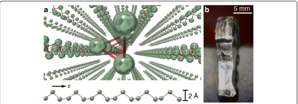
Two exemplary 1D weakly bonded materials are tri-gonal Se and Te, which have lattices consisting of spiral chains oriented along thec-axis, each spiral having three atoms per turn with adjacent chains arranged hexago-nally (Fig. 1). The chains are bound together to form a single crystal through the van der Waals force [18] or perhaps more accurately as a weakly bonded solid [19]. In this letter, we report mechanical exfoliation of tri-gonal Te single crystals to obtain nanoscale Te flakes and wires, which demonstrate the potential for fabrica-tion of single atom chains and a new platform for 1D electronics and photonics.
While there are many 1D weakly bonded materials from which to choose, several properties of isolated Se
* Correspondence:[email protected]
1Department of Physics, University of Arkansas, Fayetteville, AR 72701, USA 2Institute for Nanoscience and Engineering, University of Arkansas,
Fayetteville, AR 72701, USA
Full list of author information is available at the end of the article
and Te semiconductor atom chains set them apart from other 1D atomic layered materials. For example:
1. They are predicted to have direct semiconducting band gaps of 1 and 2 eV for Te and Se, respectively, with strongly thickness-dependent band gaps [19], creating new opportunities for tiny, wavelength-tunable detectors and emitters.
2. The helical structure of Se and Te chains is expected to confer unique electrical, optical, and mechanical properties, including novel spin-orbit coupling ef-fects boosted by heavy Se and Te atoms [20], nega-tive compressibility and band gap narrowing under pressure and strain [21], and extraordinary flexibility greater than typical elastic polymers [22].
3. Since they are composed of a single element, an isolated Se or Te atom chain would have the smallest diameter of any known 1D material. The height of the triangular spiral cross-section is 2 Å, and the inter-chain distance is 3.4 Å [23].
Experimental demonstration of the atom chain con-cept originates with STM manipulation of individual atoms on a substrate to achieve linear and planar arrays of coupled atoms [24, 25]. In addition to atom-by-atom assembly on surfaces, step edges of substrates have been decorated with atom chains [26], and self-assembled growth has been used to create large-area arrays of atom chains [27]. However, depending on the approach, all these pioneering experiments do not allow 1D structures to be created over large scales, choice of materials is lim-ited, or the structure is strongly bound to the substrate. In principle atom chains derived from 1D weakly bonded materials could overcome these limitations.
To date, the anisotropic structure of Se and Te has permitted growth of small diameter nanowires [28, 29],
self-assembly of single chains inside zeolite pores [30, 31] and carbon nanotubes [32], the growth of 2D mono-layer trigonal Te on graphene [33], and solution-growth of 2D Te [34, 35]. This earlier work demonstrates the tendency of Te to form chains and nanowires that are relatively stable mechanically and chemically outside the bulk Te crystal structure. Our objective is to use exfoli-ation of solid Te as a route to obtain single atom chains.
Methods
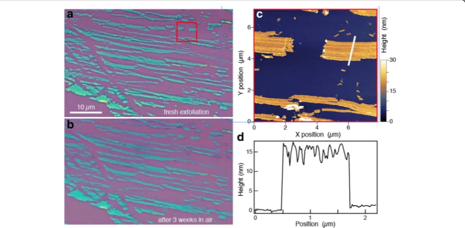
To provide evidence for the potential for fabrication of single atom chains, we investigated Te rather than Se because of the availability of large, high-quality Te single crystals [36]. Prior to exfoliation, silicon substrates with 90 or 300 nm of thermal oxide were sonicated in acet-one and isopropanol, then treated with oxygen plasma to improve adhesion of Te. Trigonal Te single crystals were mechanically exfoliated, without tape, directly on the silicon substrates [37] by manually sliding a freshly cleaved facet of Te on the substrate. We obtained the best results with the c-axis perpendicular to the direc-tion of modirec-tion. For Te exfoliadirec-tion, we have found this method to be significantly superior to tape exfoliation, which likely reflects an important difference in the bonding between 1D and 2D layered materials. Thin Te flakes were identified by contrast in an optical micro-scope (Fig. 2a). Thin Te flakes show up with a progres-sion of colors in reflected light microscopy with the thinnest crystals appearing as darker greens and blues on this silicon substrate.
Results and Discussion
Tellurium was exfoliated in anisotropic linear bands with lengths up to 50 μm (Fig. 2a). Atomic force microscopy of some of these bands reveals heights in the 10–15 nm range (Fig. 2c), with ridges running along the length of
[image:2.595.57.540.87.255.2]the bands that are evident in both the height image and a height profile taken perpendicular to one of the bands as shown in Fig. 2d. The modulated surface pattern and vari-ation in wire width are evidence that the atom chains ran-domly break away from the bulk crystal both laterally and vertically, unlike 2D layered materials such as graphene which exfoliate with mostly flat surfaces whether a tape or sliding technique is used. We were able to obtain wires of 1–2 nm thickness using this sliding technique.
For example, the atomic force images of the second sample reveal a similar anisotropic structure of the exfo-liated material (Fig. 3a), as well as significantly narrower Te nanowires with heights in the subnanometer range (Fig. 3b–d) or at least corresponding to two to four chains for an inter-chain distance of 3.4 Å [23]. These ultrathin Te nanowires have lengths of 100–200 nm (Fig. 3a). A height profile taken along thec-axis direction (green line in Fig. 3b, green curve in Fig. 3d) indicates that the surface roughness along the top of this 2–3-nm tall nanowire is comparable to or less than that of the SiO2substrate.
Stability in ambient environment is a concern for any newly exfoliated material because surface reactions that are negligible in bulk materials can dominate the proper-ties of ultrathin exfoliated materials. An optical image of the same Te sample in Fig. 2a is shown in Fig. 2b after storage for 3 weeks in air. Aside from differences in color contrast due to camera settings, the aged sample appears virtually the same as when it was freshly exfoli-ated. In particular, we note a complete absence of the blistering that occurs when 2D black phosphorus
degrades in air [38]. This observation is consistent with the observation that the timescale for degradation of Te nanowires in various solvents such as water is not indef-inite but quite long, from hours to days [39].
We further characterize the exfoliated Te by Raman spectroscopy. The Raman spectrum of bulk Te at room temperature is dominated by two sets of modes: an A1 singlet at 120 cm−1and a pair of E doublets at 92 (104) and 141 (141) for transverse (longitudinal) phonons [40]. The A1and E modes of trigonal Te may be visualized as symmetric and antisymmetric breathing modes of the triangular cross-section of the Te chain [41]. This spectrum is reproduced in Fig. 4a for an excitation wave-length of 633 nm, with the lower E mode absent because of the polarization direction of the incident light [42]. Peak positions agree with those reported in Ref. [40] to better than 1 cm−1. We note that excitation at 633 nm is near a resonance with the dielectric function of bulk Te; off-resonant excitation at 532 nm produces significantly less Raman scattering intensity [43].
The Raman spectrum of an approximately 30-nm-thick Te flake (red circle in Fig. 3a) shows the same two peaks, shifted to slightly higher frequencies (Fig. 4a). The measured Raman peak of the silicon substrate at 520.9 cm−1(not shown) indicates that the spectrometer is calibrated to better than 1 cm−1. We also note that the exfoliated Te spectrum shown in Fig. 4a, which was measured in air several weeks after exfoliation, is not consistent with the Raman spectra of either amorphous [44] or oxidized Te [45], which also establishes the en-vironmental stability of ultrathin exfoliated Te. Despite a
Fig. 2aTe exfoliated on a Si/SiO2 substrate, imaged immediately after exfoliation.bThe same sample as in (a) after storage in air for 3 weeks.c
[image:3.595.62.538.89.323.2]slight asymmetry in the Raman peaks for both bulk and exfoliated Te, a pair of Lorentzians fits the spectra rea-sonably well (black curves in Fig. 4a). Peak parameters extracted from the fits indicate a mode hardening for the exfoliated flake relative to the bulk crystal of 4 cm−1 for the A1mode and 2 cm−1for the E mode.
One interpretation of this mode hardening is a flake-substrate interaction, for example, if the Te is strained as it is exfoliated on the SiO2 substrate. Interaction with the substrate also generically hardens the radial breath-ing modes of carbon nanotubes [46]. Another possibility is that inter-chain interactions are reduced in ultrathin
a
b
Fig. 4aRaman scattering spectrum of bulk Te crystal (blue) and an exfoliated flake (red), under the same excitation conditions (633 nm, polarization parallel toc-axis). Spectra are normalized to the height of the dominant A1 peak. Fits (black curves) are a sum of two Lorentzians.
bPolar plot of Raman intensity averaged over the spectral range in (a) as a function of linear excitation polarization angle relative to thec-axis (plot origin is zero intensity). The fit is a sine function plus a constant. Theblack arrowindicates thec-axis direction (see text)
a
b
c
d
[image:4.595.63.537.86.357.2] [image:4.595.59.539.513.684.2]Te because a significant fraction of chains is missing one or more neighbors. A naïve expectation would be that weaker inter-chain coupling would soften the A1mode; however, applying pressure to Te crystals is known to re-duce the A1frequency [47]. Further, the A1frequency of isolated Te chains inside zeolite nanopores, where inter-chain coupling is zero (or significantly less than for bulk, considering the 6.6 Å nanopore diameter), is much higher than in bulk Te at 172 cm−1 [48]. The observa-tion that reduced inter-chain coupling hardens Te Ra-man modes is explained by a competition between inter-and intra-chain forces in Ref. [23]. Our measurement of a smaller shift for the E mode than the A1 mode (Fig. 4a) is also consistent with the pressure dependence re-ported in Ref. [43], but substrate-induced strain may be expected to produce similar behavior. We are unable to conclude within the scope of this work whether sub-strate interaction or reduced inter-chain interactions are responsible for the spectral shifts we observe.
For the sample shown in Fig. 3, both optical and atomic force microscopy display elongated, horizontally aligned Te flakes, which suggests that the c-axis of the Te crystal is horizontal in these images. However, the AFM images (Fig. 3b, c) also show that a significant frac-tion of the exfoliated flakes, particularly the thinnest ones, are tilted 45° away from horizontal. To confirm the crystal orientation of this sample, we use polarization-resolved Raman spectroscopy. The polarization of the excitation beam was rotated with a half-wave plate, and the integrated Raman intensity from 85 to 170 cm−1is shown in Fig. 4b. The intensities were normalized by the laser power under the microscope ob-jective measured at each polarization angle. The Raman intensity shows two maxima within one full rotation, lo-cated at 45° and 225° with respect to the X and Yaxes defined in the microscope images (Fig. 3). The intensity varies approximately sinusoidal (black curve in Fig. 4b), with an amplitude of +/−15% over a constant background.
Meanwhile, the optical absorption of bulk Te at 633 nm is stronger for light polarized perpendicular to the c-axis than for parallel polarization [49]. For Te flakes with nearly bulk-like optical properties (Fig. 4a), we therefore expect Raman intensity to be higher for light polarized perpendicular to thec-axis. Based on the angle of the Raman maximum in Fig. 4b, we conclude that the Te nanowires oriented at 45° in Fig. 3b, c are elongated parallel to thec-axis for that sample. Because different Te flakes on the same substrate were used for Raman spectroscopy and AFM, an assumption of this conclusion is that the crystal axes are the same for all exfoliated flakes shown in Fig. 3a. This assumption would not be appropriate for flakes prepared by the traditional tape exfoliation method, but it is a reasonable
assumption for the unidirectional rubbing technique used here. These observations demonstrate that polar-ized Raman spectroscopy is sufficient to determine the crystal orientation of nanoscale exfoliated Te. This tech-nique is useful in practice given that optical and atomic force microscopy do not provide unambiguous informa-tion about crystal orientainforma-tion. As the thickness and width of exfoliated Te approaches the single atom chain limit, we expect a cross-over in the crystal direction as-sociated with maximum Raman scattering because iso-lated Te chains inside nanopores have maximum Raman intensity for polarization parallel to thec-axis [48].
Conclusions
We have introduced trigonal Te as a weakly bonded ma-terial capable of being exfoliated to produce ultrathin Te single crystals. We demonstrate that the atom chain structure of Te allows it to be exfoliated as two-dimensional flakes and one-two-dimensional nanowires. Atomic force microscopy of exfoliated Te shows that thicknesses of 1–2 nm and wires of about 100 nm width can be exfoliated with this method. The Raman modes of exfoliated Te match those of bulk Te, with a slight shift (4 cm−1) due to a hardening of the A1and E modes. Polarized Raman spectroscopy is used to determine the crystal orientation of exfoliated Te flakes. These experi-ments establish exfoliation as a route to achieve nano-scale trigonal Te while demonstrating the potential for fabrication of single atom chains of Te. Our current ef-forts are focused on producing Te or Se single atom chains by molecular beam epitaxy or by improving exfoliation.
Acknowledgements
We acknowledge J. M. grant for graphical assistance. This work was supported by AFOSR award numbers 14-1-0205 (S.-Q.Y.) and FA9550-16-1-0203 (H.C.). H. C. acknowledges support from the University of Arkansas Connor Faculty Fellowship.
Availability of Data and Materials
The corresponding author (HC) should be contacted regarding requests for data and materials.
Authors’Contributions
HC, GS, and SQY conceived of the experiment and directed the research. IS grew the Te single crystals. HC and TH produced exfoliated Te samples. HC, TH, XH, and JS and acquired the data. HC, TH, and GS analyzed the data. HC, GS, and SQY wrote the manuscript with input from all authors. All authors read and approved the final manuscript.
Ethics Approval and Consent to Participate
Not applicable.
Consent for Publication
Not applicable.
Competing Interests
Publisher’s Note
Springer Nature remains neutral with regard to jurisdictional claims in published maps and institutional affiliations.
Author details
1Department of Physics, University of Arkansas, Fayetteville, AR 72701, USA. 2Institute for Nanoscience and Engineering, University of Arkansas,
Fayetteville, AR 72701, USA.3Department of Electrical Engineering, University of Arkansas, Fayetteville, AR 72701, USA.4Department of Electrical and
Computer Engineering, McGill University, Montreal, QC H3A 0G4, Canada.
Received: 15 June 2017 Accepted: 27 July 2017
References
1. Jorio A, Dresselhaus G, Dresseldhaus MS, editors (2008) Carbon nanotubes. Springer, New York
2. Zhang A, Zheng G, Lieber CM (2016) Nanowires. Springer, Switzerland 3. Tans SJ, Verschueren ARM, Dekker C (1998) Room-temperature transistor
based on a single carbon nanotube. Nature 393:49
4. Cui Y, Duan X, Hu J, Lieber CM (2000) Doping and electrical transport in silicon nanowires. J Phys Chem B 104:5213
5. Kong J et al (2000) Nanotube molecular wires as chemical sensors. Science 287:622
6. Cui Y, Wei Q, Park H, Lieber CM (2001) Nanowire nanosensors for highly sensitive and selective detection of biological and chemical species. Science 293:1289
7. Liang W et al (2001) Fabry - Perot interference in a nanotube electron waveguide. Nature 411:665
8. Refael G, Heo J, Bockrath M (2007) Sagnac interference in carbon nanotube loops. Phys Rev Lett 98:246803
9. Novoselov KS et al (2004) Electric field effect in atomically thin carbon films. Science 306:666
10. Novoselov KS et al (2005) Two-dimensional gas of massless Dirac fermions in graphene. Nature 438:197
11. Zhang Y, Tan Y-W, Stormer HL, Kim P (2005) Experimental observation of the quantum Hall effect and Berry's phase in graphene. Nature 438:201 12. Novoselov KS et al (2005) Two-dimensional atomic crystals. Proc Nat Acad
Sci USA 102:10451
13. Avouris P, Heinz TF, Low, T (2017) 2D materials: properties and devices. Cambridge, New York
14. Cheon G et al (2017) Data mining for new two- and one-dimensional weakly bonded solids and lattice-commensurate heterostructures. Nano Lett 17:1915
15. Island JO et al (2017) Electronics and optoelectronics of quasi-one dimensional layered transition metal trichalcogenides. https://arxiv.org/abs/1702.01865 16. Venkataraman L, Lieber CM (1999) Molybdenum selenide molecular wires as
one-dimensional conductors. Phys Rev Lett 83:5334
17. Venkataraman L, Kim P (2006) Electron transport in a multichannel one-dimensional conductor: molybdenum selenide nanowires. Phys Rev Lett 96:076601
18. Hippel ARvon (1948) Structure and conductivity in the VIbgroup of the
periodic system. J Chem Phys 16:372
19. Joannopoulos JD, Schlüter M, Cohen ML (1975) Electronic structure of trigonal and amorphous Se and Te. Phys Rev B 11:2186
20. Entin MV, Magarill LI (2002) Electrons in a twisted quantum wire. Phys Rev B 66:205308
21. Ren W, Ye J-T, Shi W, Tang Z-K, Chan CT, Sheng P (2009) Negative compressibility of selenium chains confined in the channels of AlPO4-5
single crystals. New J Phys 11:103014
22. Flory PJ (1969) Statistical mechanics of chain molecules. Interscience, New York
23. Martin RM, Lucovsky G, Helliwell K (1976) Intermolecular bonding and lattice dynamics of Se and Te. Phys Rev B 13:1383
24. Eigler DM, Schweizer EK (1990) Positioning single atoms with a scanning tunnelling microscope. Nature 344:524
25. Yazdani A, Eigler DM, Lang ND (1996) Off-resonance conduction through atomic wires. Science 272:1921
26. Gambardella P et al (2002) Ferromagnetism in one-dimensional monatomic metal chains. Nature 416:301
27. Yeom HW et al (1999) Instability and charge density wave of metallic quantum chains on a silicon surface. Phys Rev Lett 82:4898
28. Qian HS et al (2006) High-quality luminescent tellurium nanowires of several nanometers in diameter and high aspect ratio synthesized by a poly (vinyl pyrrolidone)-assisted hydrothermal process. Langmuir 22:3830
29. Xi G et al (2006) Large-scale synthesis, growth mechanism, and photoluminescence of ultrathin Te nanowires. Cryst Growth Des 6:2567 30. Bogomolov VN (1978) Liquids in ultrathin channels (Filament and cluster
crystals). Sov Phys Usp 21:77
31. Li IL et al (2005) Resonant Raman study of confined Se single helix and Se8
rings. Appl Phys Lett 87:071902
32. Medeiros PVC et al (2017) Extreme Te nanowires encapsulated within ultra-narrow single-walled carbon nanotubes. https://arxiv.org/abs/1701.04774 33. Huang X et al (2017) Epitaxial growth and band structure of Te film on
graphene. https://arxiv.org/abs/1703.07062
34. Wang Y et al (2017) Large-area solution-grown 2D tellurene for air-stable, high-performance field-effect transistors. https://arxiv.org/abs/1704.06202 35. Du Y et al (2017) 1D van der Waals material tellurium: Raman spectroscopy
under strain and magneto-transport. https://arxiv.org/abs/1704.07020 36. Shih I, Champness CH (1978) Czochralski growth of tellurium single crystals.
J Cryst Growth 44:492
37. Navarro-Moratalla E et al (2016) Enhanced superconductivity in atomically thin TaS2. Nat Comm 7:11043
38. Wood JD et al (2014) Effective passivation of exfoliated black phosphorus transistors against ambient degradation. Nano Lett 14:6964
39. Lan W-J et al (2007) Dispersibility, stabilization, and chemical stability of ultrathin tellurium nanowires in acetone: morphology change,
crystallization, and transformation into TeO2in different solvents. Langmuir
23:3409
40. Pine AS, Dresselhaus G (1971) Raman spectra and lattice dynamics of tellurium. Phys Rev B 4:356
41. Lucovsky G (1967) The structure of amorphous selenium from infrared measurements. In: Cooper WC, editor. The physics of selenium and tellurium. Canada. P. 255–267
42. Oyobuturi TS (1971) Physical properties of tellurium. J Soc Appl Phys 40:594 43. Richter WJ (1972) Extraordinary phonon Raman scattering and resonance
enhancement in tellurium. Phys Chem Solids 33:2123
44. Brodsky MH et al (1972) The Raman spectrum of amorphous tellurium. Phys Stat Sol B 52:609
45. Mirgorodsky AP et al (2000) Dynamics and structure of TeO2polymorphs:
model treatment of paratellurite and tellurite; Raman scattering evidence for newγ- andδ-phases. J Phys Chem Solids 61:501
46. Araujo PT et al (2010) Resonance Raman spectroscopy of the radial breathing modes in carbon nanotubes. Physica E 42:1251
47. Richter W et al (1973) Hydrostatic pressure dependence of first-order Raman frequencies in Se and Te. Phys Stat Sol B 56:223
48. Poborchii VV (1996) Polarized Raman and optical absorption spectra of the mordenite single crystals containing sulfur, selenium, or tellurium in the one-dimensional nanochannels. Chem Phys Lett 251:230