N A N O E X P R E S S
Shape-Controlled Synthesis of ZnS Nanostructures: A Simple
and Rapid Method for One-Dimensional Materials by Plasma
Hu PengÆBai LiuyangÆYu LingjieÆ Li JinlinÆ Yuan FangliÆChen Yunfa
Received: 17 March 2009 / Accepted: 24 May 2009 / Published online: 4 June 2009 Óto the authors 2009
Abstract In this paper, ZnS one-dimensional (1D) nano-structures including tetrapods, nanorods, nanobelts, and nanoslices were selectively synthesized by using RF ther-mal plasma in a wall-free way. The feeding rate and the cooling flow rate were the critical experimental parameters for defining the morphology of the final products. The detailed structures of synthesized ZnS nanostructures were studied through transmission electron microscope, X-ray diffraction, and high-resolution transmission electron microscope. A collision-controlled growth mechanism was proposed to explain the growth process that occurred exclusively in the gas current by a flowing way, and the whole process was completed in several seconds. In con-clusion, the present synthetic route provides a facile way to synthesize ZnS and other hexagonal-structured 1D nano-structures in a rapid and scalable way.
Keywords Zinc sulphide 1D nanocrystal
Thermal plasma
Introduction
In the past decade, considerable effort has been paid on the preparation of 1D nanostructures such as nanorods, nano-wires, nanobelts, and nanotubes due to their potential application as building blocks for constructing a range of electronic and photonic nanodevices (such as nanolasers,
nanosensors, field-effect transistors, and nanocantilevers, etc.) [1–8]. Among these materials, 1D sulphide nano-structures have attracted great interest due to their sizes and morphology-related properties and their emerging appli-cations in functional nanodevices. For example, in nano-composite-based photovoltaics, 1D sulphide may provide paths for more efficient transport of carriers from photo-induced interfacial charge separation, and thus increase the overall photocurrent efficiency [4, 9]. Accordingly, 1D sulphide materials are not only fundamentally interesting but also highly promising in a broad range of applications and merit extensive investigation.
ZnS is an important II–VI group semiconductor com-pound with a direct band gap of 3.7 eV that exhibits wide optical transparency from the visible light (0.4lm) to the deep infrared region (12 lm), which makes ZnS as one of the most common materials used in optical and optoelec-tronic fields [10–12]. For example, ZnS is widely used to fabricate the optical windows due to its excellent optical transparency together with the chemical and thermal sta-bility [13,14]. In recent years, nanoscale structures of ZnS, particularly the quasi 1D nanostructures, have been the focus of intensive research used as building blocks for nanoelectronic and nanophotonic systems [15–20]. Because of their enhanced properties significantly different from those of their bulk counterparts and the new nanostructure-based devices nanostructure-based on these properties, synthesis and fabrication of ZnS 1D nanostructures have been the focus of increasing research, and many methods have been devel-oped to synthesize ZnS 1D nanostructures [21–24]. Among these methods, thermal evaporation has been confirmed to be a simple way to obtain ZnS 1D nanostructures with different morphology. Naoto et al. [25], reported the syn-thesis of ZnS nanostructures by simple thermal evaporation of ZnS powder in the presence of Au catalysts at 970°C, H. PengB. LiuyangY. LingjieL. JinlinY. Fangli (&)
C. Yunfa
State Key Laboratory of Multi-phase Complex System, Institute of Process Engineering, Chinese Academy of Sciences, 100190 Beijing, China
and in their case, well-controlled wurtzite ZnS nanobelts, nanosheets, and nanorods were obtained. More complex structures, such as hierarchical structured nanohelices, have also been synthesized by the thermal evaporation process in Wang’s laboratory using zinc sulfide as source material [26]. Because the supersaturation plays a key role in the morphology of final products in vapor synthesis, the prod-ucts with different shape were often obtained at different temperature zone of the same substrate, which made an obstacle to separate and collect of the products with single shape. In addition, the main limitation of their methods is the small-scale quantities with the yields no more than gram level. The long reaction time and low process pressure were the main factors that restrict these methods to scale up.
In our previous report, uniform ZnO nanorods with closely controlled aspect ratio have been successfully synthesized by the RF thermal plasma beyond gram level per minute without using any catalysts, but the products with other shape (such as nanobelts, nanowires) could not be obtained [27]. Because the zinc and sulfur could be vaporized at a relatively low temperature due to their low vapor formation points at 1,180 K for Zn and 718 K for S, respectively, it is much easier and economical to fabricate ZnS nanostructures based on the reaction between the vapors of Zn and S. In this paper, we reported that the synthesis of ZnS 1D nanostructures in a scalable way using Zn and S powder as the starting materials, and the product shape could be well controlled by adjusting the experiment parameters. The plasma synthesis process has been proved as a facile way to obtain 1D nanostructures.
Experimental Section
In the present study, a RF thermal plasma reactor operated at 30 kW was used to synthesize ZnS nanocrystals. The plasma was generated by a three-turn, water-cooled induction coil from a RF power-supply system with a frequency of 4 MHz. In the experiment process, the start-ing materials of commercial Zn and S powder (-200 mesh) were firstly mixed together (according to the mole ratio of 1:1) and then fed into the plasma through a water-cooled atomizer probe by the carrier gas (nitrogen gas, at a flow rate of 150 L/h) in a continuous way. The raw materials subsequently underwent vaporization, nucleation, and growth processes, and the final products were collected at the bottom of the collector. Argon (1.0 m3/h) and nitrogen gas (5.0 m3/h) were injected as the plasma-form-ing gas and sheath gas, respectively. The chamber pressure was maintained at atmospheric pressure. A schematic illustration of the configuration of the apparatus is available in the literature [27].
The structural characteristics of as-synthesized samples were determined using an X-ray diffractometer (XRD, Philips X’Pert PRO MPD) through the 2h-range from 10 to 90 degree at a scan rate of 0.02 deg s-1operated at 40 kV and 30 mA with Cu Karadiation. The morphology of the products was characterized using both a scanning electron microscopy (SEM, JSM-6700F) and transmission electron microscope (TEM, Hitachi H-800). The detailed mor-phology and structural characterization were investigated by a high-resolution transmission electron microscope (HRTEM) and selected-area electron diffraction (SAED) in the same transmission electron microscope (TEM, JEOL JEM-2011). Photoluminescence (PL) measurements were carried out at room temperature using 325 nm as the excitation wavelength with a luminescence spectrometer (Perkin-Elmer, LS50B).
Results and Discussions
Figure2 reveals the XRD patterns of products synthe-sized at different experimental parameters, and we can conclude that the hexagonal wurtzite ZnS with the lattice constantsa=3.82 A˚ andc=6.25 A˚ was obtained in all cases, and no diffraction peaks corresponding to Zn and S are detected in the XRD patterns. The results demonstrate the formation of well-crystallized ZnS nanostructures, but
there still have three weak diffraction peaks indexed to wurtzite ZnO detected (as marked * in the XRD pattern) in the sample, which reveals the formation of trace amounts of ZnO in the synthesized process. This is because that the nitrogen gas used in our experiment contains about 0.5% content of oxygen gas, and the oxygen has higher activity than sulfur at high temperature. When the starting materials were supplied into the plasma flame, the reaction between zinc and oxygen is prior to zinc and sulfur attributed to the thermodynamics reasons. As a result, ZnO was formed prior to ZnS. Consequently, the products we obtained were wurtzite ZnS with little amount of ZnO.
The morphology and structure of synthesized ZnS products were also studied by the TEM analysis. Low-magnified TEM images (the results without show) of the products synthesized at different experimental parameters further proved that the crystals consist of different 1D nanostructures as the SEM images shown in Fig.1. Fig-ure3 shows the magnified TEM images and their corre-sponding HRTEM images of single ZnS 1D nanostructures, respectively. Magnified TEM images of synthesized single crystals of tetrapod, nanorod, and nanobelt were shown in Fig.3a–c, from which we can see that the synthesized crystals display uniform width all less than 100 nm along their axes, while the length varied from several hundred nanometers to micrometers. Figure3d–f illustrates the HRTEM images of corresponding nanostructures shown in Fig.3a–c, revealing their perfect hexagonal wurtzite
Fig. 1 SEM images of ZnS nanostructures produced with different sets of feeding rate and cooling gas flow ratea12 g/min and without cooling gas,b24 g/ min and without cooling gas,c
21 g/min and with cooling gas 3 m3/h, andd21 g/min and with cooling gas 6 m3/h
[image:3.595.183.546.58.347.2] [image:3.595.54.288.470.665.2]structure of ZnS. The measured spacing of the crystallo-graphic planes is about 0.625 nm, corresponding to the (001) lattice planes. The corresponding SAED taken per-pendicular to the axis of the nanostructures is shown in the inset of Fig.3d–f respectively. It, together with the HRTEM, confirms that the growth of single crystalline ZnS tetrapods and nanobelts was generally along [001] direc-tion, while the nanorods was perpendicular to [001]
direction. Although the synthesized nanostructures prefer to grow along different growth directions, they are all hexagonal elongation along the c-axis according to the theoretical and crystal habit of the ZnS.
In plasma synthesis process, the resident time of parti-cles in the plasma system is no more than several seconds, that is, the reaction time is very short. Even for the nano-belts longer than tens of micrometers, the growth is
Fig. 3 Magnified TEM images of synthesized single ZnSa
[image:4.595.183.547.55.597.2]completed in several seconds as well. One of the important features of synthesis in RF plasma system is that the growth rate is rather rapid when compared with the con-ventional vapor deposition process. In the experimental process, vapor species were formed due to the high pro-cessing temperature (up to 1.09104K) in the flame zone, and then cooled to form ultrahigh-level supersaturated vapor in the plasma tail, which provides intensive growth driver for ZnS to nucleate and grow. In addition, part of zinc was ionized in the plasma zone, which accelerates the transmittability of electrons from zinc to sulfur. All of these provide intensive growth driver for ZnS to nucleate and grow, and the 1D nanostructures were finally formed due to the anisotropic growth habit of ZnS crystals results from the cation- or anion-terminated atomic planes [26]. Different materials were also synthesized by this method in our laboratory (including previous reported ZnO, Zn, AlN, and WO3).
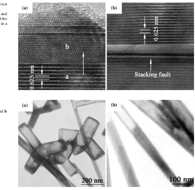
Meanwhile, rapid growth rate sometimes may cause the formation of crystal defects in crystal lattice during the growth process, and Fig.4 confirms the formation of two
different crystal defects in the final products. Figure4a illustrates the stacking fault existed in a single nanobelt, which is parallel to the axis and runs through out the nanobelt. Figure4b shows a leg of tetrapod ZnS with two types of structure zone, one consists of the wurtzite struc-ture (hcp, hexagonal close-packed) in zone a and the other is sphalerite structure (fcc, face-centered cubic) in zone b, and the two different structures were formed by changing the stacking sequence of the closed-packed planes of the ZnS crystal and resulted from the crystallogenesis of ZnS [28].
Interestingly, some hollow nanocrystals were obtained when we analyzed the products collected from the inner wall of the reactor. Figure5 shows the TEM images of obtained hollow tetrapod and tubular nanocrystals, which are resulted from the oxidation process of the ZnS nano-crystals by the atomic oxygen at high temperature. Loh et al. [29] reported the hollowing mechanism of zinc sul-fide nanowires by an atomic oxygen beam, and the oxygen atoms play key role in the formation of hollow structures. In our experiment, low concentration of oxygen gas was
Fig. 4 The crystal defects exist in the ZnS nanocrystalsa
stacking fault in a nanobelt and
bthe sphalerite structure and the wurtzite structure polytypes in a leg of tetrapod
Fig. 5 TEM images of synthesized hollow
nanostructuresatetrapod andb
[image:5.595.147.546.54.444.2]introduced into the reaction chamber continuously due to the impurity of the nitrogen gas. The oxygen gas was then heated to an ultra-high temperature and partially atomized even ionized in the plasma flame due to the effect of plasma electromagnetic field, which made oxygen possess high activity. When the atomized oxygen collided with the crystals attached on the reactor wall under high tempera-ture, the substituted reaction of S by O was occurred on the surface of the crystals, and the inner S was slowly diffused outward. Eventually, hollow nanostructures were formed after the ZnS core was removed completely, and EDX analysis also proved this point.
In the conventional vapor-solid (VS) process, evapora-tion, chemical reducevapora-tion, or gaseous reaction first generates the vapor. The vapor is subsequently transported and condensed onto a substrate, and then the nuclei are formed, continually absorbed the arrived vapor species and finally grew into 1D structures. The growth process of crystals occurs at an immovable spot, and the substrate plays a key role in the formation of 1D nanostructures. While in the plasma synthesis, this process is quite different. There is no settled spot for nuclei to deposit and grow. The starting materials are vaporized in the flame, and then undergo condensation, nucleation, and growth processes exclusively in the flowing gas current. The previously condensed vapor cannot complete the growth process by continually absorbing the latterly arrived vapor species because when the later formed vapor species arrived, the previously formed nuclei have already moved away in their falling process. Therefore, the nucleation and growth processes could only complete by colliding of different nuclei around
themselves. By this way, the condensed vapor absorbs other species and energy, completes the nucleation and growth process in the falling process, and finally forms the 1D nanostructures. Figure6 shows HRTEM image of synthesized ZnS tip, and there is no Zn metal or catalyst particles found on the tip, which further confirms that the growth process in the plasma is still a VS mechanism. Analyzing the flow conditions in our experiment reactor, it could be concluded that distribution of the stream lines in plasma reactor is mostly uniform by calculating the Reynolds’s number, which ensures the uniform environ-ment for different crystal to nucleate and grow. Accord-ingly, uniform products with singly shape were obtained in our experiment.
The PL measurement of the ZnS nanostructures was carried out with a Xe lamp at 325 nm excitation at room temperature. PL spectrum taken from the ZnS nanorods, nanowires, and tetrapods gives almost similar emission behavior, as shown in Fig.7. Three strong and broad emission bands located at 367, 453, and 487 nm have been observed. It is well known that the luminescent peak cen-tered at 367 nm could be assigned to the UV-excitonic emission [14]. The ZnS nanomaterials reported previously have PL emission with bands in the range 400–450 nm [30,31] associated with the sulfur vacancy. Therefore, the strong blue emission at around 453 nm should be assigned to the stoichiometric vacancies in the ZnS nanocrystal, and the nanobelts present high sulfur vacancy than the nano-rods and tetrapods according to intensity of the emission peaks. Another strong emission peak is located at 487 nm, which is similar to that of the well-known ZnS-related luminescence (at about 480 nm) produced by zinc vacan-cies [32]. Because the crystal growth in the plasma process
Fig. 6 HRTEM image of one tip of synthesized ZnS nanorods
Fig. 7 PL spectra of synthesized ZnS nanostructures ananobelts,
[image:6.595.53.288.463.698.2] [image:6.595.307.542.494.687.2]is very rapid and the structure defects are inevitably, we reasonably believe that the green–blue luminescence is associated with the defect-related emission of the ZnS host.
Conclusions
In summary, various 1D nanostructures of ZnS, including the tetrapods, nanorods, nanobelts, and nanoslices, were successfully synthesized by the thermal evaporation of zinc and sulfur powder using a plasma system. The morphology of synthesized products could be well controlled by vary-ing the feedvary-ing rate and the coolvary-ing flow rate, and the synthesized crystals display uniform width all less than 100 nm and the length varying from several hundred nanometers to micrometers. The formation mechanism of 1D nanostructures was due to the anisotropic growth habit of ZnS crystal, and the rapid growth rate of plasma syn-thesis process also caused the formation of crystal defects in the products. In addition, this method provides a facile way to synthesize ZnS and other wurtzite-structured 1D nanostructures in a scalable and continuous way.
Acknowledgments This work was supported financially by the National High Technology Research and Development Program of China (863) (No. 2008AA03Z308).
References
1. Z.L. Wang,Nanowires and Nanobelts-Materials, Properties and Devices: Nanowires and Nanobelts of Functional Materials (Tsinghua University Press, Beijing, 2004)
2. C.L. Yan, D.F. Xue, Adv. Mater.20, 1055 (2008). doi:10.1002/ adma.200701752
3. L. Li, Y. Zhang, Y.W. Yang, X.H. Huang, J.G. Li, L.D. Zhang, Appl. Phys. Lett.87, 31912 (2005). doi:10.1063/1.2000327 4. M. Law, J. Goldberger, P.D. Yang, Annu. Rev. Mater. Res.34, 83
(2004). doi:10.1146/annurev.matsci.34.040203.112300
5. B.X. Wang, D.F. Xue, J. Solid State Chem. 180, 1028 (2007). doi:10.1016/cj.jssc.2006.12.033
6. J.Y. Lao, J.Y. Huang, D.Z. Wang, Z.F. Ren, Nano. Lett.3, 235 (2003). doi:10.1021/nl025884u
7. J.S. Xu, D.F. Xue, J. Phys. Chem. B 110, 11232 (2006). doi: 10.1021/jp061274x
8. M.S. Arnold, P. Avouris, Z.W. Pan, Z.L. Wang, J. Phys. Chem. B
107, 659 (2003). doi:10.1021/jp0271054
9. W.U. Huynh, J.J. Dittmer, A.P. Alivisatos, Science295, 2425 (2002). doi:10.1126/science.1069156
10. P.V. Natarajan, D.G. Vaiude, B.M. Rao, Hybrid Circuits27, 28 (1992)
11. M. Bredol, J.J. Merichi, Mater. Sci.33, 471 (1998). doi:10.1023/ A:1004396519134
12. P. Calandra, M. Goffredi, V.T. Liveri, Colloids Surf.A Physico-chem. Eng. Asp. 160, 9 (1999). doi:10.1016/S0927-7757(99) 00256-3
13. S. Musikant,Optical Materials—An Introduction to Selection & Application(Marcel Dekker, New York, 1985)
14. H.J. Yuan, S.S. Xie, D.F. Liu, X.Q. Yan, Z.P. Zhou, L.J. Ci, J.X. Wang, Y. Gao, L. Song, L.F. Liu, W.Y. Zhou, G. Wang, J. Cryst. Growth258, 225 (2003). doi:10.1016/S0022-0248(03)01502-1 15. J.Q. Hu, Y. Bando, J.H. Zhan, D. Golberg, Adv. Funct. Mater.15,
757 (2005). doi:10.1002/adfm.200400084
16. S. Kar, S. Chaudhuri, J. Phys. Chem. B109, 3298 (2005). doi: 10.1021/jp045817j
17. C.J. Barrelet, Y. Wu, D.C. Bell, C.M. Lieber, J. Am. Chem. Soc.
125, 11498 (2003). doi:10.1021/ja036990g
18. Q.H. Xiong, G. Chen, J.D. Acord, X. Liu, J.J. Zengel, H.R. Gutierrez, J.M. Redwing, L.C. Lew Yan Voon, B. Lassen, P.C. Eklund, Nano. Lett.4, 1663 (2004). doi:10.1021/nl049169r 19. X. Fan, X.M. Meng, X.H. Zhang, W.S. Shi, W.J. Zhang, J.A.
Zapien, C.S. Lee, S.T. Lee, Angew. Chem. Int. Ed. 45, 2568 (2006). doi:10.1002/anie.200504069
20. X.S. Fang, L.D. Zhang, J. Mar. Sci. Technol.22, 721 (2006) 21. X.C. Jiang, Y. Xie, J. Lu, L.Y. Zhu, W. He, Y.T. Qian, Chem.
Mater.13, 1213 (2001). doi:10.1021/cm0006143
22. Q.S. Wu, N.W. Zheng, Y.P. Ding, Y.D. Li, Inorg. Chem. Com-mun.5, 671 (2002). doi:10.1016/S1387-7003(02)00523-3 23. X.J. Chen, H.F. Xu, N.S. Xu, F.H. Zhao, W.J. Lin, G. Lin, Y.L.
Fu, Z.L. Huang, H.Z. Wang, M.M. Wu, Inorg. Chem.42, 3100 (2003). doi:10.1021/ic025848y
24. J.F. Gong, S.G. Yang, H.B. Huang, J.H. Duan, H.W. Liu, X.N. Zhao, R. Zhang, Y.W. Du, Small 2, 732 (2006). doi:10.1002/ smll.200500419
25. C.H. Liang, Y. Shimizu, T. Sasaki, H. Umehara, N. Koshizaki, J. Phys. Chem. B108, 9728 (2004). doi:10.1021/jp037963f 26. D. Moore, Y. Ding, Z.L. Wang, Angew. Chem. Int. Ed.45, 5150
(2006). doi:10.1002/anie.200600429
27. P. Hu, F.L. Yuan, L.Y. Bai, J.L. Li, Y.F. Chen, J. Phys. Chem. C
111, 194 (2007). doi:10.1021/jp065390b
28. Y. Jiang, X.M. Meng, J. Liu, Z.Y. Xie, C.S. Lee, S.T. Lee, Adv. Mater.15, 323 (2003). doi:10.1002/adma.200390079
29. M. Lin, J. Zhang, C. Boothroyd, Y.L. Foo, M. Yeadon, K.P. Loh, J. Phys. Chem. B108, 9631 (2004). doi:10.1021/jp0485284 30. J.F. Suyver, S.F. Wuister, J.J. Kelly, A. Meijerink, Nano. Lett.1,
429 (2001). doi:10.1021/nl015551h
31. W.G. Becker, A.J. Bard, J. Phys. Chem.87, 4888 (1983). doi: 10.1021/j150642a026