NAN O R EVIE W
Open Access
Graphene-based optical modulators
Siyuan Luo
1,2, Yanan Wang
1, Xin Tong
1and Zhiming Wang
1,2*Abstract
Optical modulators (OMs) are a key device in modern optical systems. Due to its unique optical properties, graphene has been recently utilized in the fabrication of optical modulators, which promise high performance such as broadband response, high modulation speed, and high modulation depth. In this paper, the latest experimental and theoretical demonstrations of graphene optical modulators (GOMs) with different structures and functions are reviewed. Particularly, the principles of electro-optical and all-optical modulators are illustrated. Additionally, the limitation of GOMs and possible methods to improve performance and practicability are discussed. At last, graphene terahertz modulators (GTMs) are introduced.
Keywords:Graphene; Optical modulator; Photonics; Absorption; Electro-absorption; All-optical; Terahertz; Broadband; Ultrafast
Review Introduction
As one of the key components in photonics systems, an optical modulator is a device used to control the funda-mental characteristics of a carrier light propagating in free space or in an optical waveguide upon an external elec-tronics/photonics signal [1]. In order to meet specific re-quirements in applications, such as modern lasers, optical communication, and terahertz communication, various designs have been demonstrated. And thanks to the latest development in nanotechnology and material science, advanced-function materials are progressively involved in device fabrication. For instance, group III-V materials [2], germanium [3,4], polymers [5,6], and graphene [7,8] have been applied and incorporated to silicon-based modula-tors to form hybrid devices, with the aim to improve the modulation speed, broaden the modulation range, and re-duce the device footprint and energy consumption. Accord-ing to the parameters beAccord-ing modulated, these devices can be categorized as amplitude, phase, or polarization modulators. Generally, amplitude modulation is the most common due to its classified system. And the performance can be charac-terized by optical bandwidth, modulation depth, modulation
speed, insertion loss, area efficiency (footprint), and power consumption [9].
As the prime material for the semiconductor industry, silicon modulators have to be fabricated in large scale to obtain enough modulation depth, due to a relatively weak high-order electro-optical effect. On the other hand, modu-lators based on germanium and other compounds have problems to be integrated with current complementary metal-oxide-semiconductor (CMOS) techniques. For mod-ulators with resonators, narrow modulation bandwidth limits their development. By contrast, graphene can cover the needs of scale, speed, and techniques. And integration with graphene can help current modulators to improve their performance.
Graphene, a single layer of hexagonally packed carbon atoms, was first isolated from graphite via mechanical exfoli-ation in 2004. For these highly confined two-dimensional crystals, in-plane carbon atoms are connected by strong σ-bonds, while adjacent layers only share weak van de Waals force. The unique crystalline structure endows graphene extraordinary electronic, optical, thermal, and mechanical properties. Graphene is expected to grow into the new sili-con in future electronics and photonics. Many proof-of-concept photonics devices based on graphene, including photodetectors [10,11], ultrafast lasers [12,13], polarization controllers [14], and plasmonic structures [15-17], have been demonstrated.
* Correspondence:[email protected]
1Institute of Fundamental and Frontier Sciences, University of Electronic
Science and Technology of China, Chengdu 610054, People’s Republic of China
2
State Key Laboratory of Electronic Thin Film and Integrated Devices, School of Microelectronics and Solid-State Electronics, University of Electronic Science and Technology of China, Chengdu 610054, People’s Republic of China
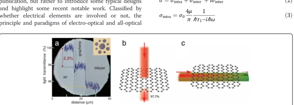
For applications in optical modulators, graphene has its unique advantages as follows: (1) High modulation speed: With a carrier mobility as high as 200,000 cm2/(V · s) at room temperature, graphene is considered as one of the fundaments of next-generation ultrafast electronics/pho-tonics devices [18]. Ultrafast (picoseconds) processes in graphene, such as photocarrier generation and relaxation, offer graphene a possibility to operate at over hundreds of GHz [19]. Thus, the Fermi level, which is directly related to the optical absorption of graphene, can be rapidly mod-ulated through gating voltage doping. (2) Wide optical bandwidth: Due to its unique electronic structure [10,11], graphene has a constant absorption of πα= 2.293% from visible to infrared wavelengths [12], whereα= e2/hcdenotes the fine-structure constant [13], as is shown in Figure 1a. This bandwidth covers the optical fiber communication bandwidth, typically from 1,300 to 1,600 nm. (3) High op-tical absorption: Considering only one atom thickness, an optical absorption of approximately 2.3%, which is approxi-mately 50 times higher than that of GaAs of the same thickness, is quite high. By integrating graphene along with a waveguide, the light-graphene interaction length can be further improved [14], as shown in Figure 1b,c. In this ori-ginal structure, an absorption (modulation depth per unit length) of 0.2 ~ 1 dB/μm can be achieved. Higher absorp-tion will help to reduce the scale of the device (footprint). (4) CMOS-compatible: During the past decade, large-scale graphene can be integrated using CMOS-compatible pro-cesses [15,16]. Moreover, because of Pauli blocking (band filling), saturable absorption has been observed [17,20], which makes it possible to fabricate all-optical graphene optical modulators.
In this review article, we provide a brief overview of graphene-based optical modulators. Our survey is not intended to cover every single device reported in prior publication, but rather to introduce some typical designs and highlight some recent notable work. Classified by whether electrical elements are involved or not, the principle and paradigms of electro-optical and all-optical
graphene optical modulators are elaborated in the‘ Electro-optical graphene Electro-optical modulator’and‘All-optical graph-eme optical modulator’sections, respectively. In addition, graphene-based material systems for THz wave modula-tion are discussed in the ‘Graphene terahertz modulator’ section. The article closes with a final conclusion and out-look in the‘Conclusions’section.
Electro-optical graphene optical modulator
Mechanism of electro-absorption
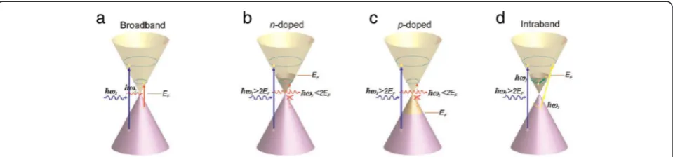
Due to the sp2hybridization of carbon atoms, graphene has a unique electronic structure in that the conduction band and valence band meet at Dirac points like two cones [10,11]. A linear energy-momentum dispersion rela-tion can be noted in the vicinity of Dirac points and car-ries behavior that can be modeled as massless Dirac fermions.
For pristine graphene, electrons can be excited by incident photons with a broad range of energies and only interband transition is permitted (Figure 2a). As a consequence of uni-versal optical conductance, the transmittance of pristine gra-phene is frequency-independent and only determined by the fine-structure constant α= e2/ħc (where e is the electronic charge,ħis Planck’s constant divided by 2π, andcis the vel-ocity of light) [13]:
T ¼ð1þ2πG=cÞ−2≈1−πα≈0:977 ð1Þ
While sufficiently doped, the optical transition of
gra-phene is mainly determined by chemical potential μ
(Fermi level EF), which can be controlled by chemical doping or electrical gating. The Kubo formula can be used to describe the dynamic response of graphene, in-cluding interband transition and intraband transition [1]:
σ¼σintraþσinter’þiσinter” ð2Þ
σintra¼σ04μπ
1
[image:2.595.58.541.512.685.2]ℏτ1−iℏω ð3Þ
Figure 1Optical absorption in graphene.(a)Optical absorption of approximately 2.3% for pristine graphene from ref. [13]. (Inset) Graphene
σinter’¼σ0 1þ
1 πarctan
ℏω−2μ
ℏτ2 −
1 πarctan
ℏωþ2μ
ℏτ2
ð4Þ
σinter”¼−σ0
1 2πln
ℏωþ2μ
ð Þ2þℏ2τ
22 ℏω−2μ
ð Þ2þℏ2τ
22
ð5Þ
Both interband transition and intraband transition are related to chemical potentialμand the frequency of inci-dent light ω. When μ=0, no intraband transition will happen. When |μ| <ħω/2, (slightly n-doped or p-doped) optical transition is dominated by interband transition. In n- and p-doped (corresponding to positive and nega-tive gating voltage) graphene, the incident photons with energy less than 2EFcannot be absorbed. This is because the electron states in the conduction band are filled up as shown in Figure 2b or there are no electrons in the valence band available for interband transition as shown in Figure 2c. Thus, if the incident light is fixed, by elec-trically tuning the Fermi level, interband transitions can be turned on and off [21,22]. When |μ| <ħ ω/2, the intraband transition related to the terahertz range will be dominant [23-25]. At this condition, plasmon mo-mentum enhancement is allowed and propagation of surface plasmon in graphene becomes possible [26-28].
In earlier theory demonstrations, graphene was treated as an isotropic material [29,30]. Graphene can transfer from dielectric-like to metallic-like when the permittivity is tuned to approach zero. Recently, graphene became well accepted as an anisotropic material. When graphene was treated as an anisotropic material [31,32], a linear relation between its in-plane permittivity and effective mode index can be observed. The electric distributions are also different in or out of graphene when it is treated as an isotropic or anisotropic material [33]. In this case, the in-plane permittivity can be tuned by the chemical potential, while the out-of-plane permittivity (in a direc-tion perpendicular to the graphene sheet) does not [33].
Basic designs of electro-optical graphene optical modulator (GOM)
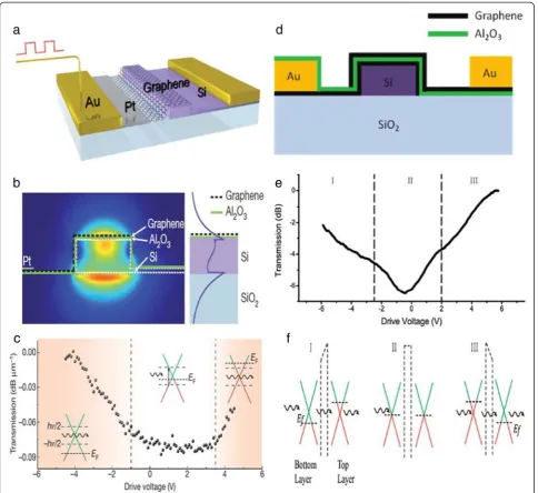
[image:3.595.59.539.89.201.2]In 2011, Liu et al. first experimentally demonstrated a GOM by integrating a monolayer graphene sheet on a Si waveguide as shown in Figure 3a [7]. The waveguide propagates light and graphene will offer absorption. The field distribution of the propagating light is shown in Figure 3b, which is very important to modulation depth. External gating voltage was used to control the Fermi level of graphene and resulted in changes of transmis-sion in the Si waveguide as shown in Figure 3c. This ori-ginal modulator can work at a broad bandwidth from 1,350 to 1,600 nm, which covers the wavelength of the optical fiber communication system we are using today. A modulation depth per unit length of 0.1 dB/μm was achieved, and the footprint of this modulator was 25μm2. Right after the first demonstration, they further improved the modulator by integrating double-layer gra-phene on the top of a Si waveguide [8], as is shown in Figure 3d. This double-layer GOM has a similar trans-mission property to that of the single-layer GOM in their former work, as is shown in Figure 3e. The two graphene layers with a p-oxide-n-like structure are sim-ultaneously absorptive or transparent for incident light, as is shown in Figure 3f. As is expected, a higher modu-lation depth of 0.16 dB/μm was observed due to the double-layer graphene, which implies a smaller footprint at 3-dB modulation. This performance is comparable to that of traditional optical modulators made of Si [9] and GeSi [34].
Advanced structures for electro-optical GOM
With the aim to achieve higher performance, different structures have been developed. High modulation depth not only brings a higher signal quality but also helps to re-duce the footprint. Simply increasing the peak-to-peak gate voltage swing can achieve high modulation depth at the expense of increased power consumption. Improving the graphene-light interaction can fundamentally increase the performance. Similar to Liu et al.’s work, Koester and Li
Figure 2Possible optical transitions in graphene.(a)Optical transition in pristine graphene.(b)Optical transition in n-doped (or driven by
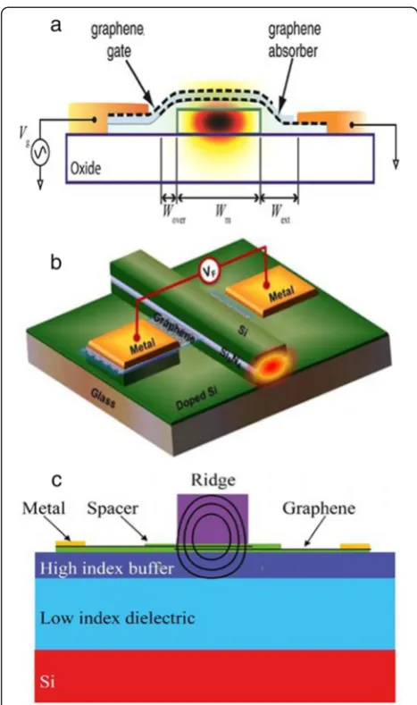
[image:3.595.67.291.258.348.2]simulated a graphene-on-silicon structure [35] as shown in Figure 4a. Although a modulation speed of 120 GHz is pos-sible, the interaction length is 60 μm when achieving a 3-dB modulation (corresponding to 0.05 3-dB/μm). Lu and Zhao theoretically showed that graphene sheets should be placed at the maximum of the electric field [30]. They designed a structure in which the graphene sheet is
[image:4.595.57.542.88.532.2]sandwiched in the center of the waveguide as shown in Figure 4b. A modulation depth of 3.75 dB/μm was achieved, which is much higher than that of the graphene-on-silicon structure. However, placing the graphene sheet in the wave-guide is difficult to be realized. Imperfect fabrication such as mismatch of the upper part and bottom part of the wave-guide may influence the signal quality. Gosciniak and Tan
Figure 3Single-layer and double-layer GOMs.(a)Schematic of a single-layer GOM. The graphene film is separated from the silicon waveguide by
theoretically proposed a method to avoid the technique challenges and at the same time placed graphene sheets close to the maximum of the electric field [36], as is shown in Figure 4c. A Si rib waveguide was deposited on the sub-strate covering the double-layer graphene sheet. The Si waveguide was specially designed in size to form an egg-like field distribution which is represented by the black line in Figure 4c. The double-layer graphene was separated by a thin dielectric spacer forming a parallel capacitor model. Modulation depths of 5.05 dB/μm for TM mode and 0.29 dB/μm for TE mode were achieved. With this high modulation depth, nanoscale devices with 3-dB modulation depth are possible. It should be noted that in this structure, part of the mode was pushed into the buffer layer, which may make the mode field weaker. Thus, balance designa-tion is necessary. Without waveguides, transmission and
reflection structures provide different applications. Lee et al. fabricated a reflection GOM within sub-wavelength thickness [37]. Later, by improving graphene supercapaci-tors, Polat and Kocabas achieved broadband GOMs and compared the performance of transmission and reflection [38]. As is expected, the reflection structure showed a higher modulation depth. In the aspect of insertion loss, an insertion loss of 3.3 dB with a modulation of 16 dB was experimentally demonstrated, recently [39].
Integration of graphene with other optical modulators
By integrating graphene, the performance of current optical modulators can be further enhanced. Hao et al. theoretically demonstrated a Mach-Zehnder modulator with eight-layer graphene embedded [31], as is shown in Figure 5a. The em-bedded graphene sheets significantly enhanced the electro-refraction, which is helpful to reduce the footprint to 4 × 30 μm2 and modulation arm length of 27.57 μm in the Mach-Zehnder modulator. And they further reduced the modulation arm length to 16.5μm [32]. Moreover, graphene also helps to reduce the chirp in the Mach-Zehnder modu-lator [29]. The graphene-embedded design also benefits the ring modulator. An optical modulator based on the critical coupling concept [40] can be realized when assisted by gra-phene [41]. With the driving voltage lower than 1.2 V, this modulator was compatible with low-voltage CMOS technol-ogy. Recently, Du et al. demonstrated a ring modulator with a shift rate of 1.08 nm/V at resonance peak, which is two orders of magnitude higher than that of current ring modu-lators [42], as is shown in Figure 5b. By simulating a graphene-silica permittivity-tunable metamaterial, a GOM with a footprint of 0.01μm2was reported recently [43], as is shown in Figure 5c.
In addition, a device integrating both GOMs and a graphene optical photodetector was experimentally demonstrated [44]. Recently, Zhou et al. first theoretic-ally found a quasilinear relation between the phase change and chemical potential of graphene, which im-plied an optical phase modulator [45].
RC constant limit in electro-optical GOM
In theory, the high carrier mobility of graphene will lead to an ultrahigh modulation speed. However, in experimen-tal demonstration, the modulation speed is still limited at approximately 1 GHz [7,8] lower [39] in electro-optical GOMs. The reason is the ‘electrical bottleneck’ - RC constant. The electronic circuit of this device can be equivalent to RC low-pass filter (LPF). The 3 dB cut-off frequency of electronic signal can be calculated by f = 1/
[image:5.595.56.290.86.481.2]2πRC, whereRis the total cascade resistance andCis the total capacitance between counter electrodes. These fac-tors can be measured by a network analyzer. The all-optical method is an efficient way to avoid this bottleneck.
Figure 4GOM with double-layer graphene at different positions.(a)
All-optical graphene optical modulator
The future optical fiber communication system requires a modulator whose operation speed is larger than 100 Ghz [46]. Although the graphene-based modulator has the potential to obtain a modulation rate of 500 GHz, the practical electro-absorption modulator based on gra-phene is limited to approximately 1 GHz due to the RC constant [7,8]. A direct method to avoid this ‘electrical bottleneck’is to make the modulator all-optical. That is, light modulates light. The all-optical graphene optical modulators demonstrated at present are based on satur-able absorption in graphene.
Mechanism of saturable absorption
Saturable absorption is a property of materials where the absorption of light is decreased to a steady level at suffi-ciently high incident light intensity [1]. This optical non-linearity is widely applied to generate short laser pulses as optical absorber in mode-locked lasers [20,47]. It is worth noting that high incident optical intensity may damage the material during absorption. Although many semiconductors such as GaAs also show saturable ab-sorption, only those whose saturable intensity is much lower than the optical damage threshold can be used in practical devices [48]. Optical devices based on graphene with high optical damage threshold have been fabricated [49]. Moreover, in saturable absorption devices, com-pared with single-walled carbon nanotubes (SWNTs) [17] or semiconductor saturable absorber mirrors (SESAMs) [50], graphene is much easier to be fabricated without band gap engineering or chirality (diameter) control.
The schematic saturable absorption process is shown in Figure 6 [51]. Excited by pump light, optical interband tran-sition occurs as shown in Figure 6a. Graphene absorbs inci-dent light regardless of wavelength. Then the thermalized photogenerated carriers will cool down and redistribute a Fermi-Dirac distribution. Electron–hole recombination and intraband phonon scattering accompany this redistribution
as shown in Figure 6b. With sufficient intensity of pump light, the conduction band and valence band will be filled up by electrons and holes, respectively. Thus, due to Pauli blocking (no two electrons can fill the same state), further absorption is blocked, achieving saturable absorption or ab-sorption blenching as is shown in Figure 6c. Above all, in this circumstance, other light whose energy is less than the pump light will not be absorbed by graphene. When pump light (high energy) and carrier light (low energy) simultan-eously transmit through graphene, sufficiently increasing the intensity of pump light can limit the absorption of carrier light. As a result, as is shown in Figure 7b,c,d, the intensity of carrier light will follow that of pump light, which implies all-optical modulation.
Basic designs of all-optical GOM
Liu et al. firstly experimentally showed all-optical modula-tion using a graphene-covered microfiber, which is compat-ible with the optical fiber system [52]. A chemical vapor deposition (CVD)-synthesized graphene film is dry trans-ferred by polydimethylsiloxane (PDMS) to cover the micro-fiber on MgF2substrate, as is shown in Figure 7a. In the substrate-supported structure, the substrate should have a low refractive index to guarantee the total reflection. Pump light (1,060 nm) and carrier (signal) light (1,550 nm) together transmit through the microfiber and the intensity of carrier light varied with pump light, as is shown in Figure 7b,c,d. In this work, a modulation speed of only 1 MHz is achieved due to the low switching frequency of pump light. A modulation depth of approximately 5 dB is achieved by single-layer graphene. And as is expected, a higher modulation depth of approximately 13 dB is achieved by double-layer graphene.
Advanced structures for all-optical GOM
[image:6.595.61.539.90.210.2]Actually, the all-optical graphene modulator is able to reach ultrafast modulation speed without RC limitation. A practical ultrafast all-optical graphene optical modulator, which is compatible with the current high-speed fiber
Figure 5Graphene-enhanced optical modulator.(a)Mach-Zehnder modulator with eight-layer graphene integrated in the arms. Reproduced
optical communication system, was fabricated by Li et al. [53]. The structure they used is a graphene-clad micro-fiber (GCM), as is shown in Figure 8a, which has been reported for mode-locked fiber lasers [54,55]. When 1,060-nm pump laser pulses (approximately 5 ns, 24 kHz) and 1,550-nm CW light were coupled to the GCM (Figure 8b, Module 2), it was found that the photo-detector cannot follow due to the slow recovery time. As is shown in Figure 8c,d, the long tail (approximately 80 ns) may mistake the ultrafast measurement of modulation speed. Considering this, successively releasing femto-second pump light and carrier light by using a delay line (Figure 8b, Module 1) and detecting the intensity of carrier light can measure the response of saturable absorption. This absorption has an ultrafast excitation and approxi-mately 2.2 ps decay time as shown in Figure 8e. The decay time include the relaxation time of carrier-carrier scatter-ing (tens to hundreds of femtoseconds) and that of carrier-phonon scattering (approximately 1 to a few picoseconds) [56-58]. This ultrafast response time implies a potential to achieve a modulation speed of approximately 200 GHz for Gaussian pulses. Finally, a modulation depth of 38% was achieved within 30-μm-long graphene.
[image:7.595.58.540.89.270.2]Theoretically, if the intensity of pump light is strong enough (lower than the optical damage threshold), gra-phene can be totally transparent to carrier light. Thus, the maximum modulation depth is determined by the optical absorption when the pump light is off, which is largely related to the interaction length and position of the graphene sheet. However, in the works above, suffi-ciently saturable absorption is not achieved and absorp-tion of carrier light is gradually varied with the changes of pump intensity as shown in the inset of Figure 8e [53]. In the aspect of transmission property, graphene integrated with a microfiber has higher absorption along
Figure 6Processes of saturable absorption in graphene.(a)Optical interband transition excited by incident light.(b)The photogenerated carriers
redistribute a Fermi-Dirac distribution.(c)Further absorption is blocked under sufficient intensity of incident light. Reproduced from ref. [50].
Figure 7Schematic of a graphene-covered microfiber structure and
[image:7.595.56.291.323.654.2]with increasing wavelength, which can be explained by higher evanescent field for longer wavelength at the gra-phene interface [59]. In addition, different polarization of the pump light can result in approximately 1 dB change of modulation depth [55].
Graphene terahertz modulator (GTM)
In the past decades, terahertz (THz) technology was found to be applied in diverse areas such as astronomy, biology/ medicine [60], communications [61], and defense [62]. Al-though numerous advances have been achieved, most of them focus on emitters and detectors. Devices like active fil-ters and modulators which can be integrated with current solid-state continuous-wave (CW) terahertz sources and de-tectors such as quantum cascade lasers [63], resonant tun-neling diode oscillators [64], Schottky diodes [65], backward diodes [66], or future graphene-based terahertz devices [67] still need to be improved [68]. As a gapless semiconductor, graphene is a natural material for long-wave applications such as THz. With the advantages mentioned in the intro-duction, graphene shows great potential in modulators and detectors [67].
The optical conductivity of graphene is determined by interband transition and intraband transition, respectively, mainly for short wavelength (infrared and visible) and long wavelength (terahertz) [23-25]. Thus, electrostatically tun-ing the density of states (DOS) available for intraband tran-sitions provides the possibility to effectively control the terahertz absorption [69,70]. As a result, large gating volt-age is usually used. A high modulation depth of >90% has been shown by employing graphene in place of a metal gate
in an AlGaAs/GaAs two-dimensional electron-gas (2DEG) terahertz modulator, which provides a modulation of <30 only [70].
Electro-optical GTM
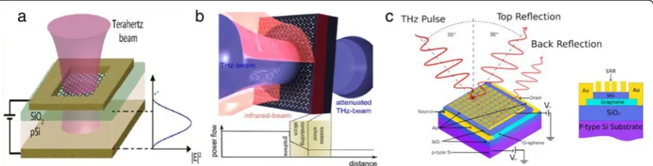
[image:8.595.60.539.91.286.2]In 2012, Sensale-Rodriguez et al. first experimentally dem-onstrated a GTM enabled only by intraband transitions [71]. Later on, they successfully used an electro-absorption GTM to control the reflectance of the terahertz wave [72]. The reflection structure they used is shown in Figure 9a. When the Fermi level in graphene is tuned to the Dirac point, intraband transition is blocked. Thus, absorption is at its minima and the reflectance of the device is at its max-ima. On the other hand, when the Fermi level shifts into the valence or conduction band of graphene, the increase of density of states available for intraband transitions leads to a higher absorption. It should be noted that if a reflection structure is used, the optical thickness of the substrate needs to be well controlled. When the substrate optical thickness is an odd-multiple of a quarter-wavelength, the electric field in graphene is maximized and absorption can be deeply modulated. On the contrary, when the sub-strate optical thickness is an even-multiple of a quarter-wavelength, the electric field in graphene disappears and absorption does not occur. As a result, a modulation depth of 64% and a low insertion loss of approximately 2 dB are achieved. Recently, they experimentally applied arrays of electro-absorption GTMs as electrically reconfigurable pat-terns for terahertz cameras [73]. A similar structure was also adopted by Lee et al. to fabricate modulators for IR range within sub-wavelength thickness [37].
Figure 8Schematic illustration and ultrafast property of all-optical graphene optical modulator.(a)Graphene-clad microfiber (GCM) structure.(b)Schematic
All-optical GTM
Following Sensale-Rodriguez et al.’s first demonstration of GTM [71], Weis et al. fabricated an all-optical GTM in the same year, 2012 [74]. They deposited graphene on silicon (GOS) to enhance the absorption as shown in Figure 9b. Upon infrared photodoping, a broadband modulation from 0.2 to 2 THz was achieved. Moreover, the modulator showed a maximum modulation depth of 99%.
GTM with resonators
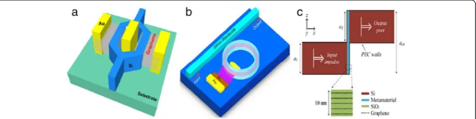
Due to accurate and deep modulation in the THz range, integration with resonators shows a way to cover special needs [75-77]. In graphene-integrated modulators, the res-onators not only enhance the interaction between gra-phene and terahertz wave but also bring the advantage to decrease the bias [78]. Degl’Innocenti et al. recently inte-grated metallic split-ring resonators (SRRs) and single-layer graphene on one substrate [79]. A modulation depth of 18% and a bandwidth from 2.2 to 3.1 THz were achieved. Additionally, the structure, as is shown in Figure 9c, showed a low bias of 0.5 V [80]. Recently, using resonators, terahertz modulators based on metamaterial and graphene have also been studied [81]. However, com-plex design and fabrication increase the difficulty and cost.
Conclusions
Optical modulators are an important device to the current and future optical systems and still need to be improved. Graphene shows great potential in fabricating broadband and ultrafast optical modulators. Optical transition includ-ing interband and intraband transitions in graphene is the main process during absorption. Electro-optical GOMs have been demonstrated while the modulation speed is lim-ited to approximately 1 GHz due to the RC constant. The position of the graphene sheet efficiently influences the light-graphene interaction. Higher modulation depth can
be easily achieved by placing graphene close to the max-imum of the electric field. Following the first demonstra-tion, many optical modulators enhanced by graphene have been theoretically and experimentally demonstrated. How-ever, higher modulation speed is necessary for current electro-optical GOMs. Driven by saturable absorption, all-optical GOMs show a potential of ultrafast modulation speed due to the ultrafast relaxation time. But direct meas-urement of ultrafast modulation has not been demon-strated. In the field of terahertz, graphene has a prominent advantage of high modulation depth. Electro-optical and all-optical modulation are both possible. In principle, theor-etical simulations go much further than experiment. GOMs with new structures and high performance tend to be dem-onstrated in the near future.
Competing interests
The authors declare that they have no competing interests.
Authors’contributions
SYL drafted the manuscript. YNW and XT revised the manuscript. ZMW carried out the review and modification. All authors read and approved the final manuscript.
Acknowledgements
This work was supported by the National Basic Research Program of China (973 Program, Grant No. 2013CB933301) and National Natural Science Foundation of China (Grant Nos. 51272038 and 51302030).
Received: 21 January 2015 Accepted: 17 March 2015
References
1. Bao Q, Loh KP. Graphene photonics, plasmonics, and broadband optoelectronic devices. ACS Nano. 2012;6:3677–94.
2. Tang Y, Peters JD, Bowers JE. Over 67 GHz bandwidth hybrid silicon electroabsorption modulator with asymmetric segmented electrode for 1.3 μm transmission. Opt Express. 2012;20:11529–35.
3. Chaisakul P, Marris-Morini D, Rouifed M-S. 23 GHz Ge/SiGe multiple quantum well electro-absorption modulator. Opt Express. 2012;20:3219–24. 4. Lever L, Hu Y, Sweeney SJ, Myronov M, IkonićZ, Liu X, et al. Modulation of
[image:9.595.62.538.90.211.2]the absorption coefficient at 1.3μm in Ge/SiGe multiple quantum well heterostructures on silicon. Opt Lett. 2011;36:4158–60.
Figure 9GTMs.(a)Electro-optical GTM. Gating voltage is applied between the top electrode and back electrode (also used to reflect the
5. Alloatti L, Korn D, Palmer R, Hillerkuss D, Li J, Barklund A, et al. 42.7 Gbit/s electro-optic modulator in silicon technology. Opt Express. 2011;19:11841–51. 6. Gould M, Baehr-Jones T, Ding R, Huang S, Luo J, Jen AK-Y, et al.
Silicon-polymer hybrid slot waveguide ring-resonator modulator. Opt Express. 2011;19:3952–61.
7. Liu M, Yin X, Ulin-Avila E, Geng B, Zentgraf T, Ju L, et al. A graphene-based broadband optical modulator. Nature. 2011;474:64–7.
8. Liu M, Yin X, Zhang X. Double-layer graphene optical modulator. Nano Lett. 2012;12:1482–5.
9. Reed GT, Mashanovich G, Gardes FY, Thomson DJ. Silicon optical modulators. Nat Photon. 2010;4:518–26.
10. Novoselov KS, Geim AK, Morozov SV, Jiang D, Katsnelson MI, Grigorieva IV, et al. Two-dimensional gas of massless Dirac fermions in graphene. Nature. 2005;438:197–200.
11. Zhou SY, Gweon GH, Graf J, Fedorov AV, Spataru CD, Diehl RD, et al. First direct observation of Dirac fermions in graphite. Nat Phys. 2006;2:595–9. 12. Mak KF, Sfeir MY, Wu Y, Lui CH, Misewich JA, Heinz TF. Measurement of the
optical conductivity of graphene. Phys Rev Lett. 2008;101:196405. 13. Nair RR, Blake P, Grigorenko AN, Novoselov KS, Booth TJ, Stauber T, et al.
Fine structure constant defines visual transparency of graphene. Science. 2008;320:1308.
14. Li H, Anugrah Y, Koester SJ, Li M. Optical absorption in graphene integrated on silicon waveguides. Appl Phys Lett. 2012;101:111110.
15. Kim KS, Zhao Y, Jang H, Lee SY, Kim JM, Kim KS, et al. Large-scale pattern growth of graphene films for stretchable transparent electrodes. Nature. 2009;457:706–10.
16. Bae S, Kim H, Lee Y, Xu X, Park JS, Zheng Y, et al. Roll-to-roll production of 30-inch graphene films for transparent electrodes. Nat Nanotechnol. 2010;5:574–8.
17. Hasan T, Sun Z, Wang F, Bonaccorso F, Tan PH, Rozhin AG, et al. Nanotube-polymer composites for ultrafast photonics. Adv Mater. 2009;21:3874–99. 18. Bolotin KI, Sikes KJ, Jiang Z, Klima M, Fudenberg G, Hone J, et al. Ultrahigh
electron mobility in suspended graphene. Solid State Commun. 2008;146:351–5.
19. Kampfrath T, Perfetti L, Schapper F, Frischkorn C, Wolf M. Strongly coupled optical phonons in the ultrafast dynamics of the electronic energy and current relaxation in graphite. Phys Rev Lett. 2005;95:187403. 20. Sun Z, Hasan T, Torrisi F, Popa D, Privitera G, Wang F, et al. Graphene
mode-locked ultrafast laser. ACS Nano. 2010;4:803–10.
21. Wang F, Zhang Y, Tian C, Girit C, Zettl A, Crommie M, et al. Gate-variable optical transitions in graphene. Science. 2008;320:206–9.
22. Li ZQ, Henriksen EA, Jiang Z, Hao Z, Martin MC, Kim P, et al. Dirac charge dynamics in graphene by infrared spectroscopy. Nat Phys. 2008;4:532–5. 23. Winnerl S, Orlita M, Plochocka P, Kossacki P, Potemski M, Winzer T, et al. Carrier relaxation in epitaxial graphene photoexcited near the Dirac point. Phys Rev Lett. 2011;107:237401.
24. Choi H, Borondics F, Siegel DA, Zhou SY, Martin MC, Lanzara A, et al. Broadband electromagnetic response and ultrafast dynamics of few-layer epitaxial graphene. Appl Phys Lett. 2009;94:172102.
25. Dawlaty JM, Shivaraman S, Strait J, George P, Chandrashekhar M, Rana F, et al. Measurement of the optical absorption spectra of epitaxial graphene from terahertz to visible. Appl Phys Lett. 2008;93:131905.
26. Mikhailov S, Ziegler K. New electromagnetic mode in graphene. Phys Rev Lett. 2007;99:016803.
27. Koppens FH, Chang DE, de Abajo FJG. Graphene plasmonics: a platform for strong light-matter interactions. Nano Lett. 2011;11:3370–7.
28. Jablan M, Buljan H, SoljačićM. Plasmonics in graphene at infrared frequencies. Phys Rev B. 2009;80:245435.
29. Yang L, Hu T, Hao R, Qiu C, Xu C, Yu H, et al. Low-chirp high-extinction-ratio modulator based on graphene-silicon waveguide. Opt Lett. 2013;38:2512–5. 30. Lu Z, Zhao W. Nanoscale electro-optic modulators based on graphene-slot.
J Opt Soc Am B. 2012;29:1490–6.
31. Hao R, Du W, Chen H, Jin X, Yang L, Li E. Ultra-compact optical modulator by graphene induced electro-refraction effect. Appl Phys Lett. 2013;103:061116. 32. Du W, Hao R, Li E-P. The study of few-layer graphene based Mach–Zehnder
modulator. Opt Commun. 2014;323:49–53.
33. Hao R, Jin J, Wei X, Jin X, Zhang X, Li E. Recent developments in graphene-based optical modulators. Frontiers of Optoelectronics. 2014;7:277–92. 34. Liu J, Beals M, Pomerene A, Bernardis S, Sun R, Cheng J, et al.
Waveguide-integrated, ultralow-energy GeSi electro-absorption modulators. Nat Photon. 2008;2:433–7.
35. Koester SJ, Li M. High-speed waveguide-coupled graphene-on-graphene optical modulators. Appl Phys Lett. 2012;100:171107.
36. Gosciniak J, Tan DT. Theoretical investigation of graphene-based photonic modulators. Sci Rep. 2013;3:1897.
37. Lee C-C, Suzuki S, Xie W, Schibli TR. Broadband graphene electro-optic modulators with sub-wavelength thickness. Opt Express. 2012;20:5264–9. 38. Polat EO, Kocabas C. Broadband optical modulators based on graphene
supercapacitors. Nano Lett. 2013;13:5851–7.
39. Mohsin M, Schall D, Otto M, Noculak A, Neumaier D, Kurz H. Graphene based low insertion loss electro-absorption modulator on SOI waveguide. Opt Express. 2014;22:15292–7.
40. Yariv A. Critical coupling and its control in optical waveguide-ring resonator systems. IEEE Photonic Technol Lett. 2002;14:483–5.
41. Midrio M, Boscolo S, Moresco M, Romagnoli M, Angelis CD, Locatelli A, et al. Graphene-assisted critically-coupled optical ring modulator. Opt Express. 2012;20:23144–55.
42. Du W, Li E-P, Hao R. Tunability analysis of a graphene-embedded ring modulator. IEEE Photonic Technol Lett. 2014;26:2008–11.
43. Yang L, Hu T, Shen A, Pei C, Yang B, Dai T, et al. Ultracompact optical modulator based on graphene-silica metamaterial. Opt Lett. 2014;39:1909–12.
44. Youngblood N, Anugrah Y, Ma R, Koester SJ, Li M. Multifunctional graphene optical modulator and photodetector integrated on silicon waveguides. Nano Lett. 2014;14:2741–6.
45. Zhou F, Hao R, Jin X-F, Zhang X-M, Li E-P. A graphene-enhanced fiber-optic phase modulator with large linear dynamic range. IEEE Photonic Technol Lett. 2014;26:1867–70.
46. Alduino A, Paniccia M. Wiring electronics with light. Nat Photon. 2007;1:153–5.
47. Song Y-W, Jang S-Y, Han W-S, Bae M-K. Graphene mode-lockers for fiber lasers functioned with evanescent field interaction. Appl Phys Lett. 2010;96:051122.
48. Keller U. Recent developments in compact ultrafast lasers. Nature. 2003;424:831–8.
49. Xiong Y, Yan L, Si J, Yi W, Ding W, Tan W, et al. Cascaded optical limiter with low activating and high damage thresholds using single-layer graphene and single-walled carbon nanotubes. J Appl Phys. 2014;115:083111.
50. Keller U, Weingarten KJ, Kartner FX, Kopf D, Braun B. Semiconductor saturable absorber mirrors (SESAM’s) for femtosecond to nanosecond pulse generation in solid-state lasers. IEEE J Sel Top Quantum Electr.
1996;2:435–53.
51. Bao Q, Zhang H, Wang Y, Ni Z, Yan Y, Shen ZX, et al. Atomic-layer graphene as a saturable absorber for ultrafast pulsed lasers. Adv Funct Mater. 2009;19:3077–83.
52. Liu Z-B, Feng M, Jiang W-S, Xin W, Wang P, Sheng Q-W, et al. Broadband all-optical modulation using a graphene-covered-microfiber. Laser Phys Lett. 2013;10:065901.
53. Li W, Chen B, Meng C, Fang W, Xiao Y, Li X, et al. Ultrafast all-optical graphene modulator. Nano Lett. 2014;14:955–9.
54. Jinzhang W, Zhengqian L, Min Z, Chenchun Y, Hongyan F, Zhiping C, et al. Evanescent-light deposition of graphene onto tapered fibers for passive Q-switch and mode-locker. IEEE Photonics J. 2012;4:1295–305.
55. He X, Liu Z-B, Wang DN. Wavelength-tunable, passively mode-locked fiber laser based on graphene and chirped fiber Bragg grating. Opt Lett. 2012;37:2394–6.
56. Dawlaty JM, Shivaraman S, Chandrashekhar M, Rana F, Spencer MG. Measurement of ultrafast carrier dynamics in epitaxial graphene. Appl Phys Lett. 2008;92:042116.
57. Sun D, Wu Z-K, Divin C, Li X, Berger C, de Heer W, et al. Ultrafast relaxation of excited Dirac fermions in epitaxial graphene using optical differential transmission spectroscopy. Phys Rev Lett. 2008;101:157402.
58. Huang L, Hartland GV, Chu LQ, Luxmi, Feenstra RM, Lian C, et al. Ultrafast transient absorption microscopy studies of carrier dynamics in epitaxial graphene. Nano Lett. 2010;10:1308–13.
59. Tong L, Lou J, Mazur E. Single-mode guiding properties of subwavelength-diameter silica and silicon wire waveguides. Opt Express. 2004;12:1025–35. 60. Siegel PH. Terahertz technology in biology and medicine. IEEE Trans
Microwave Theory. 2004;52:2438–47.
61. Federici J, Moeller L. Review of terahertz and subterahertz wireless communications. J Appl Phys. 2010;107:111101.
63. Kumar S, Chan CWI, Hu Q, Reno JL. A 1.8-THz quantum cascade laser operating significantly above the temperature ofħω/kB. Nat Phys. 2011;7:166–71.
64. Suzuki S, Asada M, Teranishi A, Sugiyama H, Yokoyama H. Fundamental oscillation of resonant tunneling diodes above 1 THz at room temperature. Appl Phys Lett. 2010;97:242102.
65. Liu L, Hesler JL, Xu H, Lichtenberger A, M WeikleII R, MWeikleII R. A broadband quasi-optical terahertz detector utilizing a zero bias Schottky diode. IEEE Microw Wirel Compon Lett. 2010;20:504–6.
66. Zhang Z, Rajavel R, Deelman P, Fay P. Sub-micron area heterojunction backward diode millimeter-wave detectors with 0.18 pW/Hz1/2noise equivalent power. IEEE Microw Wirel Compon Lett. 2011;21:267–9. 67. Hartmann RR, Kono J, Portnoi ME. Terahertz science and technology of
carbon nanomaterials. Nanotechnol. 2014;25:16.
68. Chen HT, O'Hara JF, Azad AK, Taylor AJ. Manipulation of terahertz radiation using metamaterials. Laser Photonics Rev. 2011;5:513–33.
69. Maeng I, Lim S, Chae SJ, Lee YH, Choi H, Son JH. Gate-controlled nonlinear conductivity of Dirac fermion in graphene field-effect transistors measured by terahertz time-domain spectroscopy. Nano Lett. 2012;12:551–5. 70. Sensale-Rodriguez B, Fang T, Yan R, Kelly MM, Jena D, Liu L, et al. Unique
prospects for graphene-based terahertz modulators. Appl Phys Lett. 2011;99:113104.
71. Sensale-Rodriguez B, Yan R, Kelly MM, Fang T, Tahy K, Hwang WS, et al. Broadband graphene terahertz modulators enabled by intraband transitions. Nat Commun. 2012;3:780.
72. Sensale-Rodriguez B, Yan R, Rafique S, Zhu M, Li W, Liang X, et al. Extraordinary control of terahertz beam reflectance in graphene electro-absorption modulators. Nano Lett. 2012;12:4518–22.
73. Sensale-Rodriguez B, Rafique S, Yan R, Zhu M, Protasenko V, Jena D, et al. Terahertz imaging employing graphene modulator arrays. Opt Express. 2013;21:2324–30.
74. PeterWeis G-PJL, Ho M, Rahm M. Spectrally wide-band terahertz wave modulator based on optically tuned graphene. ACS Nano. 2012;6:9118–24. 75. Chen HT, Padilla WJ, Zide JMO, Gossard AC, Taylor AJ, Averitt RD. Active
terahertz metamaterial devices. Nature. 2006;444:597–600.
76. Chen H-T, Padilla WJ, Cich MJ, Azad AK, Averitt RD, Taylor AJ. A metamaterial solid-state terahertz phase modulator. Nat Photon. 2009;3:148–51. 77. Tao H, Padilla WJ, Zhang X, Averitt RD. Recent progress in electromagnetic
metamaterial devices for terahertz applications. IEEE J Sel Top Quantum Electr. 2011;17:92–101.
78. Valmorra F, Scalari G, Maissen C, Fu W, Schonenberger C, Choi JW, et al. Low-bias active control of terahertz waves by coupling large-area CVD graphene to a terahertz metamaterial. Nano Lett. 2013;13:3193–8. 79. Degl’Innocenti R, Jessop DS, Shah YD, Sibik J, Zeitler JA, Kidambi PR, et al.
Terahertz optical modulator based on metamaterial split-ring resonators and graphene. Opt Eng. 2014;53:057108.
80. Degl’Innocenti R, Jessop DS, Shah YD, Sibik J, Zeitler JA, Kidambi PR, et al. Low-bias terahertz amplitude modulator based on split-ring resonators and graphene. ACS Nano. 2014;8:2548–54.
81. He X-j, Li T-y, Wang L, Wang J-m, Jiang J-x, Yang G-h, et al. Electrically tunable terahertz wave modulator based on complementary metamaterial and graphene. J Appl Phys. 2014;115:17B903.
Submit your manuscript to a
journal and benefi t from:
7Convenient online submission
7Rigorous peer review
7Immediate publication on acceptance
7Open access: articles freely available online
7High visibility within the fi eld
7Retaining the copyright to your article