N A N O E X P R E S S
Open Access
Interface traps and quantum size effects on the
retention time in nanoscale memory devices
Ling-Feng Mao
Abstract
Based on the analysis of Poisson equation, an analytical surface potential model including interface charge density for nanocrystalline (NC) germanium (Ge) memory devices with p-type silicon substrate has been proposed. Thus, the effects of Pbdefects at Si(110)/SiO2, Si(111)/SiO2, and Si(100)/SiO2interfaces on the
retention time have been calculated after quantum size effects have been considered. The results show that the interface trap density has a large effect on the electric field across the tunneling oxide layer and leakage current. This letter demonstrates that the retention time firstly increases with the decrease in diameter of NC Ge and then rapidly decreases with the diameter when it is a few nanometers. This implies that the interface defects, its energy distribution, and the NC size should be seriously considered in the aim to improve the retention time from different technological processes. The experimental data reported in the literature support the
theoretical expectation.
Keywords:Interface trap; Nanocrystalline; Quantum-size effect; Memory; Retention time
Background
The performance and reliability of metal-oxide semi-conductor is significantly influenced by the quality of the grown Si/SiO2 interface. The interface trap as a function of energy in the Si band gap exhibits two peaks, 0.25 and 0.85 eV for Si(110)/SiO2 interface [1] and 0.31 and 0.84 eV for Si(111)/SiO2 interface [2]. The Pbcenter resides on flat surfaces (terraces), not at ledges [3]; it is considered as the main source of defects at the Si(111)/SiO2 interface. It was named as Pb0 with reference to the Pb1 center on Si(100). The interface defect is amphoteric that is a donor level below mid gap and an acceptor level above mid gap. Memory structures based on nanocrystalline (NC) semiconductor have received much attention for next-generation nonvolatile memory devices due to their ex-tended scalability and improved memory performance [4-6]. Recently, the quantum size effects caused by the channel material NC Si neglecting the interface charge on the threshold voltage of thin-film transistors with-out float gate [7] and on charging the dynamics of NC memory devices [8] have been studied. Here, both the
quantum size effects caused by the float gate material NC and the interface traps effects on the retention time of memory devices are studied.
Theory
For p-type silicon, Poisson's equation can be written as follows:
∂2ψ ∂x2 ¼−
q
εs
NA e−
qψ kT−1
−n2i NA e
qψ kT−1
ð1Þ
where φ(z) is the electrostatic potential, εsis the dielec-tric constant of silicon,NAis the ionized acceptor concen-trations, ni is the intrinsic density, k is the Boltzmann constant, and Tis the temperature. Using the relationship
∂ ∂z
∂φ
∂z
2
¼2∂∂φz∂∂2zφ2 and then integrating from 0 toφs, obtain
surface electric field at the side of silicon substrate as follows:
ES¼
ffiffiffiffiffiffiffiffiffiffiffiffiffiffiffiffiffiffiffiffiffiffiffiffiffiffiffiffiffiffiffiffiffiffiffiffiffiffiffiffiffiffiffiffiffiffiffiffiffiffiffiffiffiffiffiffiffiffiffiffiffiffiffiffiffiffiffiffiffiffiffiffiffiffiffiffiffiffiffiffiffiffiffiffiffiffiffiffiffi 2qkT NA
εs e
−qψS kT−1þqψS
kT þ n2
i
NA
ð Þ2 e
qψS kT−1−qψS
kT
r
ð2Þ
Correspondence:[email protected]
Institute of Intelligent Structure and System, School of Urban Rail Transportation, Soochow University, Suzhou 215006, China
If ψs > 0, choose the ‘+’sign (for a p-type semicon-ductor), and ifψs< 0, choose the‘−’sign. Poisson's equa-tion in the gate oxide and the NC Ge layer with uniformly stored charge densityQncper unit area can be written as follows:
∂2ψ
∂x2 ¼0 ð3Þ
∂2ψ ∂x2 ¼−
Qnc
εncdnc ð
4Þ
wherednc and εncare the thickness and the average di-electric constant of NC Ge layer, respectively. Consider boundary conditions for the case of interface charge density Qit captured by the traps at Si/SiO2 interface; thus, the electric field across the tunneling oxide layer is the following:
Eox¼−−ε
SESþQit
εox ð
5Þ
whereεoxis the dielectric constant of SiO2. The applied gate voltage of a NC flash memory device is equal to the sum of the voltage drop across the layer of NC Ge, SiO2, and p-Si:
Vg ¼−Qnc
dnc 2εncþ
dcox εox
þðεSES−QitÞ
dtox
εox þ
dnc εnc þ
dcox εox
þψS ð6Þ
wheredtox anddcox are the thickness of the tunneling oxide layer and control oxide layer, respectively. The interface charge density is obtained by multiplying the density of interface trap states (Dit) by the trap occupation probability and integrating over the bandgap [9]:
Qit ¼q
∫
Ditð ÞE F Eð ÞdE ð7Þ The Fermi-Dirac distribution function F(E) for donor interface traps is (1 + 2 exp[(EF−E)/(kT)])−1and that for the acceptor interface traps is (1 + 4 exp[(E−EF)/(kT)])−1.The leakage current can be calculated using [10]:
J¼∫∞0 qm
kT
2π2ℏ3 T Eð Þln
1þ expððEF−EÞ=kTÞ
1þ expððEF−E−qVÞ=kTÞ
dE
ð8Þ
where T(E) is the transmission coefficient calculated by solving Equation 8 using the transfer matrix method,V is the voltage drop values in the tunneling region, m* is the effective electron mass, and ħis the reduced Planck constant. The energy of the highest valence state (Ev) and the energy of the lowest conduc-tion state (Ec) for spherical NCs of the diameter d
(given in nanometer) are given by the following ex-pression [4]:
Ecð Þ ¼d Ecð Þ þ∞
11863:7
d2þ2:391dþ4:252 ðmeVÞ ð9Þ
Evð Þ ¼d Evð Þ∞−
15143:8
d2þ6:465dþ2:546 ðmeVÞ ð10Þ
The mean diameter (d) of NC Ge is uniquely
con-trolled by the nominal thickness (t) of the deposited amorphous Ge using molecular beam epitaxy according to the law d≅ Kt (K approximately 7), and the average density of NC GeDNC≅6 × 10⁻³/t2[5]. Thus, the filling factor that is the ratio of area of NC Ge to total area can be obtained as 0.2349. The size-dependent dielectric constant can be obtained as follows [6]:
εð Þ ¼d 1þðεb−1Þ= 1þð2d0=dÞ1:1
ð11Þ
where εb is dielectric constant of bulk Ge. The charac-teristic radius for Ge is 3.5 nm. Considering the fill fac-tor, the average dielectric constant of NC Ge layer can be estimated using parallel capacitor treatment.
The top of the valence band of p-type silicon bends up-ward (ψs< 0 andΕs< 0) which causes an accumulation of majority carriers (holes) near the interface. Thus, the interface traps capture more holes when the float gate has been charged with electrons [9]. It results that the electric field across the tunneling oxide layer increases according to Equation 5, the transmission coefficient through the tunneling oxide layer increases, and the retention time de-creases. Whereas, the top of the valence band of n-type silicon bends upward which causes a depletion of majority carriers (electrons) near the interface, and the interface traps capture less holes or capture electrons if the band bends even more so that the Fermi is level below mid gap [9]. Thus, it results that the electric field across the tunnel-ing oxide layer decreases, the transmission coefficient de-creases, and the retention time increases. Additionally, such a method is still valid for metal (or other semicon-ductor) NC memory in just using their equations to sub-stitute Equations 9, 10, and 11 for NC Ge.
Methods
The transfer matrix method used in the calculation of the transmission coefficient for the tunneling current can be described as the following. The transmission co-efficientT(Ex) was calculated by a numerical solution of the one-dimensional Schrödinger equation. A parabolic
each boundary, the transmission coefficient is then found by:
T Eð Þ ¼ m0 mNþ1
kNþ1
k0 detM
j j
M22
j j2 ð12Þ
whereM is a 2 × 2 product matrix, M22 is the quantity of the second row, and the second column in this matrix
M¼
∏
Nl¼0Mlwith transfer matricesMlgiven by:
Ml¼
1 2
1þSl
ð Þexp½−i kð lþ1−klÞxl ð1−SlÞexp½−i kð lþ1þklÞxl
1−Sl
ð Þexp½þi kð lþ1−klÞxl ð1þSlÞexp½þi kð lþ1−klÞxl
ð13Þ
In Equation 13, Sl=ml+ 1kl/mlkl+ 1, and the effective masses and momenta were discretized as ml=m*[(xl−1+
xl)/2] andkl=k[(xl−1+xl)/2], respectively,xlbeing the pos-ition of lth boundary. The Fermi-Dirac distribution was used in the tunneling current calculations, and the max-imum of the longitudinal electron energy was set at 20kBT above the conduction band.
Results and discussion
The effective electron mass 0.5 m0 of SiO2, 0.26 m0 of silicon, 0.12m0of NC Ge [11] and the relative dielectric constant of the SiO2, Si, and Ge of 3.9, 11.9, and 16, re-spectively, have been used in calculations [12]. The pub-lished electron affinities of crystalline silicon, SiO2, and Ge are 4.05, 0.9, and 4.0 eV, respectively [13]. The thick-ness of the tunneling oxide layer and control oxide layer are 4 and 25 nm, respectively. NA is 1 × 1015 cm−3, the temperature is 300 K, and the silicon substrate and gate are grounded in the following calculations.
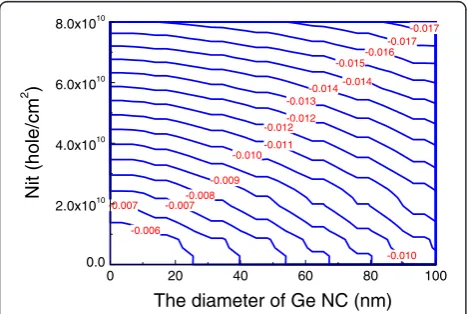
The band banding becomes smaller with decreased stored electron in the NC Ge layer and leads to a decrease in the accumulation hole density [9]. A positive interface charge density leads to an increase in the electric field across the tunneling oxide layer, which is shown in Figure 1.
It demonstrates that the electric field increases with the in-crease in the diameter of NC Ge at a stored charge in NC Ge layer of−1 × 10¹²C. Similarly, we can prove that nega-tive interface charge density will lead to a decrease in the electric field across the tunneling oxide layer. Figure 1 can be explained according to Equation 5 becauseψs< 0,Εs< 0 andQit> 0 whenVg= 0.
As we know, Pbdefects at the Si and SiO2interface for different silicon orientations have different characteris-tics [1]. Using the interface state energy distribution for the no H-passivation reported in [1], its effects on the discharging dynamics have been depicted in Figure 2. This figure clearly demonstrates that different silicon orientations have effects on the discharge dynamics whend= 8.4 nm and inset for d= 35 nm. A very small difference between those for Si(111) and Si(110) origins from the smaller difference between their leakage current (the largest relative difference is 3.3%) but in-creases with time. This is because at the initial stage, the quantity of the charge escaped from the NC Ge layer
-0.017 -0.017 -0.016 -0.015 -0.014 -0.014 -0.013 -0.012 -0.012 -0.011 -0.010 -0.010 -0.009 -0.008 -0.007 -0.007 -0.006
0 20 40 60 80 100
0.0 2.0x10¹⁰ 4.0x10¹⁰ 6.0x10¹⁰ 8.0x10¹⁰ Nit (hole/cm 2 )
[image:3.595.307.539.89.240.2]The diameter of Ge NC (nm)
Figure 1The contour of the voltage across the tunneling oxide layer.
10-6 10-5 10-4 10-3 10-2 10-1 100 101 0.0 0.2 0.4 0.6 0.8 1.0 1.2
Electron per nanodot
Discharge time (s)
1.5x10⁻⁹ 2.0x10⁻⁹ Leakage current 107 108 109 0.0 0.2 0.4 0.6 0.8 1.0
Electron per nanodot: 111 110 100
Electron per nanodot
Discharge time (s)
3.0x10⁻¹⁸ 4.0x10⁻¹⁸ 5.0x10⁻¹⁸ Leakage current: 111 110
[image:3.595.57.291.549.706.2]100 Leakage current
Figure 2Electron per NC and leakage current (A/cm2) as a function of time for different orientations.
20 40 60 80 100
0 1x10⁹ 2x10⁹ 3x10⁹ 4x10⁹ 5x10⁹ Retention time Si(111) Si(110) Si(100)
Retention time (s)
The diameter of Ge NC (nm)
3x10¹⁰ 4x10¹⁰ 5x10¹⁰ 6x10¹⁰
Qit: Si(111) Si(110)
Si(100) Q
it
(c/cm
2 )
[image:3.595.306.540.562.705.2]compared to the total quantity which is so small that the relative change cannot be observed from the figure.
The results for Si(100) can be easily explained because of the larger leakage current difference from those for Si (111) and Si(110). The leakage current exponentially in-creases due to a large increase in the Ec according to Equation 9 that leads to the leakage current exponen-tially increase. It implies that the ratio of the effects of interface charge on the leakage current to that of theEc becomes smaller, and thus, the difference between those for different silicon orientations become smaller with the decrease in the diameter of NC. Whatever they have is the same trend for the different diameters.
Figure 3 shows that the retention time firstly increase then decreases with the decrease in the diameter of NC when it is a few nanometers. The retention time is de-fined as 50% of the charges escaped from the NC Ge layer. As a comparison, the interface charge density for different silicon orientations and diameter is also depicted. It can be found that the Si(100)/SiO2 inter-face have the largest retention time due to the mini-mum leakage current. This figure illustrates that avoiding the size of NC Ge less than 4 nm can improve retention time when every NC is charged with one elec-tron. Note that the average density of NC Ge is in-versely proportional to the square of the thickness of NC Ge layer; it implies that smaller dimension of NC Ge layer stores more electrons for the case of per NC having one electron. Further, Ec changes slowly when the NC is tens of nanometers; whereas, it changes very fast when it is a few nanometers and leads a large re-duction in the barrier height according to Equation 9 and linearly decreases with interface charge. Thus, the phenomenon of the retention time which firstly in-creases, then decreases with the decrease in the diam-eter, can be explained. The experimental data is that the average retention time is larger than 90 s when the average diameter of the nanocrystals is 8 nm with a standard deviation of 2.1 nm [14,15], whereas the re-tention time is smaller than 70 s when the average diameter of the nanocrystals is 5.67 nm with a standard deviation of 1.31 nm [16]. They qualitatively support the theoretical expectation.
Conclusions
In conclusion, the effects of Pb defects at Si(100)/SiO2 interface for different silicon orientations on the dis-charging dynamics of NC Ge memory devices have been theoretically investigated. The results demonstrate that the Si(100)/SiO2 interface have the best discharge dy-namics, and Si(110)/SiO2and Si(111)/SiO2interface are nearly same. It is also found that the retention time firstly increases, then decreases with the decrease in the
diameter of NC when it is a few nanometers. The results also demonstrate that the effects of the interface traps on the discharge dynamics of NC Ge memory devices should be seriously taken into account. The experimen-tal data reported in the literature [14,15] support the theoretical expectation.
Competing interests
The author declares that he/she has no competing interests.
Authors’information
Ling-Feng Mao received the Ph.D degree in Microelectronics and Solid State Electronics from the Peking University, Beijing, People's Republic of China, in 2001. He is a professor in Soochow University. His research activities include modeling and characterization of quantum effects in MOSFETs,
semiconductors and quantum devices and the fabrication and modeling of integrated optic devices.
Acknowledgements
The author acknowledges financial support from the National Natural Science Foundation of China under Grant 61076102 and Natural Science Foundation of Jiangsu Province under Grant BK2012614.
Received: 31 July 2013 Accepted: 23 August 2013 Published: 29 August 2013
References
1. Thoan NH, Keunen K, Afanas’ev VV, Stesmans A:Interface state energy
distribution and Pbdefects at Si(110)/SiO2 interfaces: comparison to
(111) and (100) silicon orientations.J Appl Phys2011,109:013710.
2. Hurley PK, Stesmans A, Afanas’ev VV, O’Sullivan BJ, O’Callaghan E:Analysis
of Pbcenters at the Si(111)/SiO2 interface following rapid thermal
annealing.J Appl Phys2003,93:3971.
3. Stesmans A, Van Gorp G:Maximum density of Pbcenters at the
(111) Si/SiO2 interface after vacuum anneal.Appl Phys Lett1990,
57:2663.
4. Akca IB, Dâna A, Aydinli A, Turan R:Comparison of electron and hole
charge–discharge dynamics in germanium nanocrystal flash memories.
Appl Phys Lett2008,92:052103.
5. Hdiy AE, Gacem K, Troyon M, Ronda A, Bassani F, Berbezier I:Germanium nanocrystal density and size effects on carrier storage and emission.
J Appl Phys2008,104:063716.
6. Weissker H-C, Furthmüller J, Bechstedt F:Optical properties of Ge and Si nanocrystallites from ab initio calculations. II. Hydrogenated
nanocrystallites.Phys Rev B2002,65:1553282.
7. Mao LF:Quantum size impacts on the threshold voltage in
nanocrystalline silicon thin film transistors.Microelectron Reliab. in press.
8. Mao LF:Dot size effects of nanocrystalline germanium on charging
dynamics of memory devices.Nanoscale Res Lett2013,8:21.
9. Sze SM, Kwok, Ng K:Physics of Semiconductor Devices.New York: Wiley; 2007:213–215.
10. Ando Y, Itoh T:Calculation of transmission tunneling current across
arbitrary potential barriers.J Appl Phys1987,61:1497.
11. Adikaari AADT, Carey JD, Stolojan V, Keddie JL, Silva SRP:Bandgap enhancement of layered nanocrystalline silicon from excimer laser
crystallization.Nanotechnology2006,17:5412.
12. Yue G, Kong G, Zhang D, Ma Z, Sheng S, Liao X:Dielectric response and its
light-induced change in undoped a-Si:H films below 13 MHz.Phys Rev B
1998,57:2387.
13. Matsuura H, Okuno T, Okushi H, Tanaka K:Electrical properties of
n-amorphouslp/p-crystalline silicon heterojunctions.J Appl Phys1984,
55:1012.
14. Teo LW, Ho V, Tay MS, Choi WK, Chim WK, Antoniadis DA, Fitzgerald EA: Dependence of nanocrystal formation and charge storage/retention performance of a tri-layer insulator structure on germanium
concentration and tunnel oxide thickness.InThe 4th Singapore-MIT
15. Teo LW, Choi WK, Chim WK, Ho V, Moey CM, Tay MS, Heng CL, Lei Y, Antoniadis DA, Fitzgerald EA:Size control and charge storage mechanism of germanium nanocrystals in a metal-insulator-semiconductor structure.
Appl Phys Lett2002,81:3639.
16. Kan EWH, Koh BH, Choi WK, Chim WK, Antoniadis DA, Fitzgerald EA: Nanocrystalline Ge flash memories: electrical characterization and trap
engineering.InThe 5th Singapore-MIT Alliance Annual Symposium: January
19-20, 2005; Singapore.
doi:10.1186/1556-276X-8-369
Cite this article as:Mao:Interface traps and quantum size effects on the retention time in nanoscale memory devices.Nanoscale Research Letters20138:369.
Submit your manuscript to a
journal and benefi t from:
7Convenient online submission
7Rigorous peer review
7Immediate publication on acceptance
7Open access: articles freely available online 7High visibility within the fi eld
7Retaining the copyright to your article