MODELLING AND ANALYSIS OF PARALLEL BOOST
CONVERTER FOR PHOTOVOLTIC APPLICATIONS
T.AJITH BOSCO RAJ, R.RAMESH Department of Electrical and Electronics Engineering,
Anna University, Chennai, India.
[email protected]@annauniv.edu
ABSTRACT
The main objective of this paper is to develop a mathematical modelling and design a high efficient photovoltaic (PV) application with proposed parallel boost converter. This model is based on mathematical equations and is described through an equivalent circuit including a PV source with MPPT, a diode, a series resistor, a shunt resistor and a dual boost converter with active snubber circuit. This model can extract PV power and boost by using dual boost converter with active snubber. By using this method the overall system efficiency is improved and also the switching losses is reduced.
Key Words: MPPT, SEPIC Converter, PV module, Parallel Boost Converter
1. Introduction
Solar power is a renewable energy source that might replace fossil fuel dependent energy sources. However, for that to happen, solar power cost per kilowatt-hour has to be competitive with fossil fuel energy sources. Currently, solar panels are not very efficient, it has 12-20% efficiency to convert sunlight to electrical power. The efficiency can drop further due to other factors such as solar panel temperature and load conditions. In order to maximize the power derived from the solar panel, it is important to operate the panel at its optimal power point. To achieve this, a type of charge controller called a Maximum Power Point Tracker should be designed and implemented.
The MATLAB/PSPICE model of the PV module is developed [1-4] to study the effect of temperature and insolation on the performance of the PV module. MATLAB-based modelling and simulation
scheme which is suitable for studying the I–V and
P–V characteristics of a PV array under a
non-uniform insolation due to partial shading [5] was proposed. The mathematical model of solar PV module is useful for the computer simulation. The power electronics interface connected between a solar panel and a load or battery bus, is a pulse width modulated (PWM) DC-DC converter or their derived circuits is used to extract maximum power from solar PV panel[6]. The main drawback of PV systems is that the output voltage of PV panels is
highly dependent on solar irradiance and ambient temperature. Therefore it is not possible to connect the PV panels outputs directly to the load. To improve this, a DC-DC boost converter is required to interface between PV panels and loads [7]. The boost converter decides the output voltage of the PV system. Converter receives the variable input voltage which is the output of PV panels and give up constant output voltage across its output capacitors where the loads can be connected. In general, a DC-DC boost converter operates at a certain duty cycle. In this case, the output voltage depends on that duty cycle. If the input voltage is changed while the duty cycle is kept constant, the output voltage will vary. Duty cycle is varied by using a pulse width modulation (PWM) technique [8].
Silicon carbide (SiC) represents an advanced silicon technology because it allows a larger energy gap. SiC is classified as a wide-band-gap (WBG) material, and it is the mainstream material for
power semiconductors [9] [10]. Among the
proposed circuit provides perfectly ZVT turn ON and ZCT turn OFF together for the main switch of a converter by using only one quasi resonant circuit without an important increase in the cost and complexity of the converter. This paper is organized as follows. In Section 2, MATLAB model of L1235-37W Solar PV module is presented. In Section 3 Mathematical Model for Parallel Boost Converter with Active Snubber Circuit is presented and in Section 4 Proposed Parallel Boost Converter for PV application is presented. Simulation Results and Discussions are given in Section 5. Finally conclusion is presented in Section 6.
2. MATLAB MODEL OF L1235-37W SOLAR PV MODULE
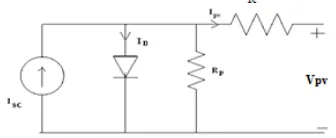
[image:2.595.305.513.299.382.2]A solar cell is the building block of a solar panel. A photovoltaic module is formed by connecting many solar cells in series and parallel. Considering only a single solar cell; it can be modelled by utilizing a current source, a diode and two resistors. This model is known as a single diode model of solar cell. Two diode models are also available but only single diode model is considered here [1],[2],[4],[17],[18] [19].The equivalent circuit of PV module is shown in figure 1.
Figure 1: Equivalent Circuit of Solar PV Module
From the figure 1, the current equation is given by
Isc = ID + IPV + (VD / Rp) (1)
Vpv=VD–(Ipv*Rs) (2)
Where diode current is, Id = Io + (e (VD / VT) - 1). The load current is given by
p pv pv
pv sc
R RI V ( 1 NKT
) RI V ( q exp I I
I − +
− + −
=
(3)
In this equation Ipv denotes the photo voltaic current, Isc is the diode reverse saturation current, q is the electron charge, Vpv is the diode across the voltage, K is the Boltzmann’s constant. T is the temperature of the junction, N is the diode identity factor, R and Rp are the series and shunt resistors of the solar cell. The complete physical behaviour of the PV cell depends upon Isc, Ipv, R ,Rp and with
two environmental parameters as the temperature and solar radiation. The model is developed in MatLab/simulink based on the above equations. For a given radiation, temperature, R and Rp, the I-V and P-V curves are generated [20]. Based on the electrical equation (1) and (2), the solar PV module is modelled in MATLAB shown in figure 2, which is used to enhance the understanding and predict
the V-I characteristics and to analyze the effect of
[image:2.595.102.270.446.515.2]temperature and irradiation variation. If irradiance increases, the fluctuation of the open-circuit voltage is very small. But the short circuit current has sharp fluctuations with respect to irradiance. However, for a rising operating temperature, the open-circuit voltage is decreased in a Non-linear fashion [1]
Figure 2: MATLAB Model for Single PV Module
The V-I characteristics are validated experimentally in the L1235-37Wp solar module shown in figure 3. The table I shows the technical specifications of L1235-37W solar module under test. The figure 4 shows the V-I characteristics based on the experimental results under irradiation
(G) =1000W/m2, temperature =25ᵒC.
[image:2.595.331.490.491.596.2]Table I: Specifications of L1235-37W Single Solar PV Panel
Short circuit current (Isc) 2.5A
Voltage at MPP(Vm) 16.4
Current at MPP(Im) 2.25
Open circuit voltage (Voc) 21V
Length 645mm
Width 530mm
Depth 34mm
Weight 4kg
Maximum power (Pmax) 37W
Figure 4:V-I Characteristics of L 1235-37W Solar Panel
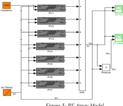
2.1 PV Array
[image:3.595.90.287.508.678.2]In order to require power an array of PV modules has been constructed. These PV modules are interconnected in series and all of them are connected to the external control block as shown in figure 5.
Figure 5: PV Array Model
The PV array model was simulated in Matlab/Simulink. The above model includes two subsystems for calculating the PV cell photocurrent which depends on the radiation and the temperature according to equation (3) [22].
[
]
1000
)
298
T
(
K
I
I
ph=
SC+
i−
β
(4)where Ki=0.0017 A/◦C is the cell's short circuit current temperature coefficient and β is the solar radiation (W/m2).
3. MATHEMATICAL MODEL FOR
PARALLEL BOOST CONVERTER
WITH ACTIVE SNUBBER CIRCUIT
Usually, boost converters are used for boosting purpose. Here two boost converters are connected in parallel. By using a parallel scheme, where inductor Lf1 and switch S1 are for main converter
while Lf2 and S2 are for active filtering. The
filtering circuit serves dual purpose as to improve the quality of line current and to reduce the total switching loss. The reduction in switching losses occurs due to different values of switching frequency and current amplitude for the two switches. The parallel connection of switch mode converter is a well known strategy. It involves phase shifting of two or more boost converters connected in parallel and operating at the same switching frequency [23]. The overall advantages of using this approach is to improve the efficiency and reliability, reduce the development cost, reduce current ripples, reduce conduction losses and reduce the size of active and passive components as boost inductor.
The purpose of Parallel Boost Converter is to avoid twice power process in two-stage scheme. Two converters can be connected in parallel to form the parallel boost scheme. Here, power from the PV to the load flows through two parallel paths. The main path is a filter, in which power is not processed, whereas the other path processes the input power. Therefore, high efficiency can be obtained by this method. The snubber circuit reduces or eliminates voltage or current spikes, enables limitation of dI/dt or dV/dt, shape the load line to keep it within the safe operating area (SOA), transfer power dissipation from the switch to a resistor or a useful load. The advantages of parallel boost converter with active snubber circuit is to improve overall efficiency, high reliability, reduced development cost due to the modular design, low harmonics and conduction loss.
consists of five inductors Lfi, Lf2, LR1, LR2, Ln and
three capacitors Cs, Cr, Co, Vg and Vo represent
supply and output voltage respectively, S (S1, S2) is an active primary switch, D (Df1, Df2) is a freewheeling diode, Ds (D1, D2, D3) is a Snubber diode and RL is the load resistance. S (S1, S2, S3) operates at a switching frequency fs with duty ratio d.
Figure 6: when S1=S2=0 and S3=1
Choose the switching frequency of switches S1=S2 =100 KHz and S3=200 KHz.
When S1=S2=0 and S3=1 as in figure 6
[
g o]
F
F
V
V
L
dt
diL
=
=
1
(5)
−
−
=
S L o F o oiL
R
V
iL
C
dt
dV
1
(6) [image:4.595.89.532.50.776.2]Also the switches S1=S2=S3=1 as in figure 7
Figure 7: when S1=S2=S3=1
[
g o]
FF
V
V
L
dt
diL
−
=
1
(7)
−
=
L o F o oR
V
iL
C
dt
dV
1
(8)Figure 8: when S1=S2=1 and S3=1 or 0
Similarly, the switches S1=S2=1 and S3=1 or 0 as in figure 8
F g F L V dt diL = (9)
−
=
L o o oR
V
C
dt
dV
1
(10)By using state–space averaging method the state equations during switch-on and switch-off conditions are F g 2 F 2 2 F 1 1 L V x L ) d 1 ( x L ) d 1 (
x& = − − − − + (11)
1 o 2 1 1 o 2 1 2 o L 2 x C ) d 1 )( d 1 ( x C d ) d 1 ( x C R 1
x& = − + − + − −
(12)
Where x1 and x2 are the moving averages of iLF and Vo respectively.
4. PROPOSED PARALLEL BOOST
CONVERTER FOR PV APPLICATION
Figure 9 shows the Block Diagram of a PV Based Parallel Boost Converter with Active Snubber. It is the combination of new active snubber circuit with parallel boost converter. Three switches are used in which switch S1 and S2 act as main switch and S3 act as an auxiliary switch. S1 and S2 are controlled by ZVT and ZCT respectively. Also S3 is controlled by ZCS. This circuit operates with the input of 148 V solar power.
Figure 9: Block Diagram of PV Based Parallel Boost Converter with Active Snubber
Assume both the Main Switches (S1 and S2) operates in the same frequency. The features of proposed parallel boost converter as follows:
• All the Semiconductors work with soft
switching in the proposed converter.
• The main switches S1 and S2 turn on with ZVT
and turn off with ZCT.
• The secondary switch turn on with ZCS and
turn off with ZCS.
• All other components of the parallel boost
converter function based on this soft switching.
• There is no additional current or voltage force
on the main switches S1 and S2.
• There is no additional current or voltage force
[image:4.595.302.524.424.524.2]• Also there is no additional current or voltage
force on the main Diodes Df1 and Df2.
• According to the ratio of the transformer, a part
of the resonant current is transferred to the output load with the coupling inductance. So there is less current stress on the secondary switch with satisfied points.
• At resistive load condition, in the ZVT process,
the main switches voltage falls to zero earlier due to decreased interval time and that does not make a problem in the ZVT process for the main switch.
• At resistive load condition, in the ZCT process,
the main switches body diode ON-state time is increased when the input current is decreased. However, there is no effect on the main switch turn-OFF process with ZCT.
• This parallel boost converter operates in
high-switching frequency.
• This converter is easily controllable because
the main and the auxiliary switches are connected with common ground.
• The most attractive feature of this proposed
converter is using ZVT and ZCT technique.
• The proposed new active snubber circuit is
easily adopted with other basic PWM converters and also in switching converters.
• Additional passive snubber circuits are not
necessary for this proposed converter.
• SIC (Silicon Carbide) is used in the main and
auxiliary diodes and so reverse recovery problem is not arise.
• The proposed active snubber circuit is also
suitable for other dc–dc converters.
4.1 Procedure for Constructing A Proposed Converter
Steps to obtain a system level modeling and simulation of proposed power electronic converter are listed below.
• Determine the state variables of the proposed
power circuit in order to write its switched state- space model, e.g., inductance current and capacitance voltage.
• Assign integer variables (ON-1 and OFF-0
state) to the proposed power semiconductor to each switching circuit.
• Determine the conditions controlling the states
of the proposed power semiconductors or the switching circuit.
• Assume the main operating modes, apply
Kirchhoff's Current law and Kirchhoff's Voltage law and combine all the required
stages into a switched state-space model, which is the desired system-level of the proposed model.
• Implement the derived equations with MatLab
Simulink.
• Use the obtained switched space-state model to
design linear or nonlinear controllers for the proposed power converter.
Perform closed-loop simulations and evaluate performance of proposed converter. The algorithm for solving the differential equations and the step size should be chosen before running any simulation. This step is only suitable in closed-loop simulations [21]
4.2 Operation of Proposed Boost Converter with Snubber Circuit
The proposed PV based converter is shown in figure 10, and it is based on a dual boost circuit where the first one (switch S1 and choke Lf1) is used as main chock of boost converter circuit and where the second one (switch S2 and choke Lf2) is used to perform an active filtering. The proposed converter applies active snubber circuit for soft switching. This snubber circuit is built on the ZVT turn-ON and ZCT turn-OFF processes of the main switches. Specification of proposed parallel boost converter with active snubber is in table II.
Figure 10: Circuit Diagram Of PV Based Parallel Boost Converter With Active Snubber With Resistive Load
The power from the solar flows through the two parallel paths. High efficiency was obtained by this method. So as to reach Soft Switching (SS) for the main and the auxiliary switches, main switches turn on with ZVT and turn off with ZCT. The proposed converter utilizes active snubber circuit for SS. This snubber circuit is mostly based on the ZVT turn-ON and ZCT turn-OFF processes of the main switch. CS is the parasitic capacitors added to the main switch S1 and the main diode Df. LR2 value is limited with (Vout / LR2) triseS2 ≤ Iimax to conduct
PV
maximum input current at the end of the auxiliary
switch rise time (triseS2) and LR1 ≥ 2LR2. To turn
OFF S1 with ZCT, the duration of tZCT is at least longer than fall time of S1 (tfallS1) tZCT≥tfall_S1. Though the main switches are in OFF state, the control signal is functional to the auxiliary switch. The parasitic capacitor of the main switch should be discharged absolutely and the main switches anti parallel diode should be turned ON. The ON-state time of the anti parallel diode is named tZVT and in this time period, the gate signal of the main switch would be applied. So, the main switch is turned ON below ZVS and ZCS with ZVT.
Whereas the main switches are in ON state and ways input current, the control signal of the auxiliary switch is applied. After the resonant starts, the resonant current should be higher than the input current to turn ON the anti-parallel diode of the main switch. The ON-state time of the anti-parallel diode (tZCT), has to be longer than the main switches fall time (tfS1). After all these terms are completed, while anti-parallel diode is in ON state, the gate signal of the main switch should be cutoff to provide ZCT for the main switch. The auxiliary switch is turned ON with ZCS for the coupling inductance limits the current rise speed.
Table II. Specification Of Parallel Boost Converter With Active Snubber
Main Inductor Lf1 750µH
Main Inductor Lf2 750µH
Upper Snubber Inductor LR1 5µH
Lower Snubber Inductor LR2 (Lm+Ld) 2µH
Magnetization Inductor LM (Ln+L0l) 3µH
Parasitic Capacitor Cs 1µF
Snubber Capacitor CR 4.7nF
Output capacitor Co 330µF/450
V
Output Load Resistance R =RL 530Ω
[image:6.595.115.478.486.634.2]The current passes through the coupling inductance, must be partial to conduct maximum input current at the end of the auxiliary switch rise time (trS3). So, the turn-ON process of the auxiliary switch with ZCS is offered. To turn OFF the auxiliary switch with ZCS, though the auxiliary switch is in ON state, the current passing through the switch should fall to zero with a new resonant. Then, the control signal will be cut-off. If CS is ignored, LR1 value should be two times added than LR2 to make the auxiliary switch current fall to zero. As the current cannot stay at zero as long as the auxiliary switch fall time (tfS3), the auxiliary switch is turned OFF nearly with ZCS.
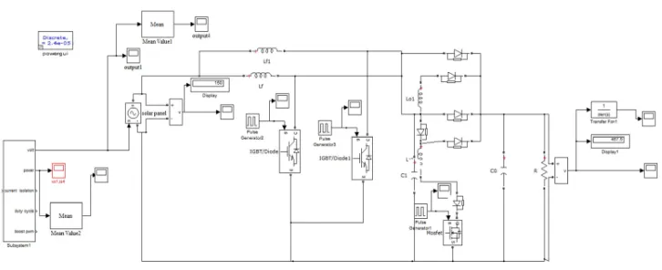
Figure 11: Simulink Model Of Proposed PV Based Parallel Boost Converter With Active Snubber Circuit
The proposed simulink topology is shown in figure 11. The inductors Lf1 & Lf2 have the similar values, the diodes Df1-Df2 are of the same type and the same guess was for the switches (S1 & S2). All inductor has its individual switch and thus it’s like the paralleling of both single/classic converters.
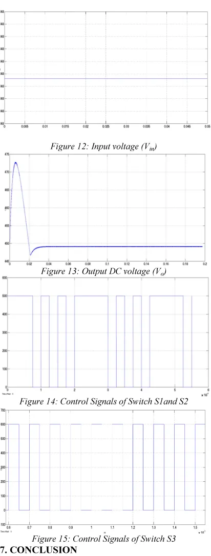
6. RESULTS AND DISCUSSIONS
simulation results show the proposed PV based soft switched parallel boost dc-dc converter has the proper response.
Figure 12: Input voltage (Vin)
Figure 13: Output DC voltage (Vo)
Figure 14: Control Signals of Switch S1and S2
Figure 15: Control Signals of Switch S3
7. CONCLUSION
The main objective of this research was to improve the efficiency of the solar PV based parallel boost converter and reduce the switching
losses. Simulations were initially done for conventional boost converter with snubber circuit. The changes in the input current waveform were obtained. A parallel boost converter was designed with soft switching which is provided by the active snubber circuit. For this idea, only one auxiliary switch and one resonant circuit was operated. The main switches and all the other semiconductors were switched by ZVT and ZCT techniques. The active snubber circuit was applied to the parallel boost converter, which is fed by solar input line. This latest converter was achieved with 148 V input and produces 448V output. The diode was added in the auxiliary switch path in order to avoid the incoming current stresses as of the resonant circuit to the main switch. As the main and the auxiliary switches have a common ground, the converter was controlled easily. The proposed new active snubber circuit can be simply functional to the further basic PWM converters and to all switching converters. Here the overall tracking efficiency is 98.6% without considering the efficiency of the solar PV panel and converter. The converter conversion efficiency is increased from 86% to 91.47%
REFERENCES
[1] Walker, G, “Evaluating MPPT converter
topologies using a MATLAB PV Model”, J.
Electr. Electron. Eng. vol. 21, no. 1, August 2001, pp. 49–56.
[2] Hiren Patel and Vivek Agarwa, “
MATLAB-Based Modeling to Study the Effects of Partial
Shading on PV Array Characteristics”, IEEE
transactions on energy conversion vol. 23, no. 1, March 2008,pp .302-310.
[3] Gow, J.A., and Manning, C.D, “Development
of a photovoltaic array model for use in power
Electronics simulation studies”, IEE
Proc.-Electr. Power Appl., vol.146, No.2, March 1999,pp.193-200
[4] Marcelo Gradella Villalva, Jonas Rafael
Gazoli, and Ernesto Ruppert Filho,
“Comprehensive Approach to Modeling and
Simulation of Photovoltaic Arrays”, IEEE
transactions on power electronics, vol. 24, no. 5, May 2009 pp.1198-1208
[5] Trishan Esram, Patrick L. Chapman,
“Comparison of photovoltaic array maximum
power point tracking techniques”, IEEE
transactions on energy conversion, vol. 22, no. 2, June 2007 pp.439-449
[6] Durán,E J., Galán, M., Sidrach-de-Cardona,
Andújar J.M, “Measuring the I-V Curve of
–dc converter topologies”, IEEE industrial electronics magazine, September 2009, pp.4-14
[7] J.Santos, F.Antunes, A.Chehab and C.Cruz, “A
maximum power point tracker for PV systems using a high performance boost converter”, Solar Energy, vol. 80, 2006, pp. 772-778.
[8] W.Jiang and B.Fahimi, “Active current sharing
and source management in fuel cell-battery
hybrid power system”, IEEE Trans. Ind.
Electron.,vol. 57, no. 2, Feb. 2010, pp. 752– 761.
[9] M.Bhatnagar and B.J.Baliga, “Comparison of 6
H-SiC, 3 C-SiC, and Si for power devices”, IEEE Trans. Electron Devices, vol. 40, no. 3, Mar. 1993, pp. 645–655.
[10]Q.Zhang, R.Callanan, M.K.Das, S.H.Ryu,
A.K.Agarwal and J.W.Palmour, “SiC power
devices for microgrids”, IEEE Trans. Power
Electron. , vol. 25, no. 12, Dec. 2010, pp. 2889–2896.
[11]A.Elasser, M.H.Kheraluwala, M.Ghezzo,
R.L.Steigerwald, N.A.Evers, J.Kretchmer and T.P.Chow, “A comparative evaluation of new silicon carbide diodes and state-of-the-art
silicon diodes for power electronic
applications”, IEEE Trans. Ind. Appl., vol. 39,
no. 4, Jul. 2003, pp. 915–921.
[12]M.M.Hernando, A.Fernandez, J.Garcia,
D.G.Lamar and M.Rascon, “Comparing Si and SiC diode performance in commercial AC-to-DC rec-tifiers with power-factor correction”, IEEE Trans. Ind. Electron. , vol. 53, no. 2, Apr. 2006, pp. 705–707.
[13] B.Ozpineci and L.M.Tolbert,
“Characterization of SiC schottky diodes at
different temperatures”, IEEE Power Electron.
Lett., vol. 1, no. 2, Jun. 2003, pp. 54–57.
[14]G.Spiazzi, S.Buso, M.Citron, M.Corradin and
R.Pierobon, “Perfor-mance evaluation of a Schottky SiC power diode in a boost PFC
applica-tion”, IEEE Trans. Power Electron.,
vol. 18, no. 6, Nov.2003, pp. 1249–1253.
[15]A.M.Abou-Alfotouh, A.V.Radun, H.Chang
and C.Winter-halter, “A 1-MHz hard-switched
silicon carbide DC–DC converter”, IEEE
Trans. Power Electron., vol. 21, no. 4, Jun.2006, pp. 880–889.
[16]B.Ozpineci, M.Chinthavali, A.Kashyap,
L.M.Tolbert and A.Mantooth,“A 55 kW three-phase inverter with Si IGBTs and SiC Schottky
diodes”, IEEE Trans. Ind. Appl., vol. 45, no. 1,
Jan./Feb. 2009, pp. 278–285.
[17]Tse.K.K., Ho.M.T., Henry S.H., Chung and
Ron Hui,S.Y, “A Novel Maximum Power
Point Tracker for PV Panels Using Switching
Frequency Modulation”, IEEE transactions on
power electronics, vol. 17, no. 6, November 2002 pp .980-989
[18]Mummadi Veerachary, “Power Tracking for
Nonlinear PV Sources with Coupled Inductor
SEPIC Converter”, IEEE transactions on
aerospace and electronic systems vol. 41, no. 3 July 2005,pp.1019-1028
[19]Tse, K.K., Billy, M. T., Ho, Henry Shu-Hung
Chung andRon Hui, S.Y, “A Comparative
Study of Maximum-Power-Point Trackers for
Photovoltaic Panels Using
Switching-Frequency Modulation Scheme”, IEEE
transactions on industrial electronics, vol. 51, no. 2, April 2004, PP.410-418.
[20]S.Daison Stallon, K.Vinoth Kumar, S.Suresh
Kumar, Justin Baby, “Simulation of High Step-Up DC–DC Converter for Photovoltaic
Module Application using
MATLAB/SIMULINK” International Journal of Intelligent Systems and Applications, 2013, vol. 07, pp.72-82.
[21]Vitor Fernao Pires, Jose Fernando A. Silva,
“Teaching Nonlinear Modeling, Simulation, and Control of Electronic Power Converters
Using MatLab/Simulink”, IEEE Transactions
on Education, Vol.45, No.3, 2002.
[22]Savita Nema, R.K. Nema, Gayatri Agnihotri,
“MATLAB/Simulink based study of
photovoltaic cells/modules/array and their
experimental verification”, International
journal of Energy and Environment, vol.1, No.3, 2010, pp.487-500.
[23]Parillo.F, “Dual Boost High Performances
Power Factor Correction (PFC) Control Strategy Implemented on A Low Cost FPGA Device, Using A Custom sfloat24 Developed
Math Library”, Universities Power