PROM·100
SDSVSTEMS
SO #7140044 REV. CPROM-lOO
PROM PROGRAMMER
COPYRIGHT 1979
UY SD SYSTEMS JULY 1979
OPERATIONS
~':\NtJAL
TARLE OF CONTENTS
C;f:CT IO~ DESCRIPTION PAGE
1-1 INTRODUCTION 1
1-2 GENERAL DESCRIPTION 1
1-3 PHYSICAL DESCRIPTION 1
1-4 SPECIFICATION 1
II FUNCTIONAL DESCRIPTION
2-1 INTRODUCTION 3
2-2 DATA OUT BUS 3
2-3 DATA !N BUS 3
2-4 A0-A7 3
2-5
1/0
CONTROL LINES 42-6 ADDRESS DECODER 4
2 - 7 OUTPUT PORT 68H 4
2-8 OUTPUT PORT 69H 4
2-9 OUTPUT PORT 6AH 4
2-10 INPUT PORT 68H 5
III CONTROL SOFTWARE
3-1 INTRODUCTION 6
3-2 2758/2716/2732 P ROG RAMlvl IN G 6
3-3 2 708 PROGRAM~lING 7
3-4 LOAD SEQUENCE 9
3-5 READ SEQUENCE 9
3-6 PROGRAMMING SEQUENCE 9
3-7 CAUTION: 10
3-8 USING THE PROM PROGRAMMER 10
3-9 LOADING AN OBJECT FILE 11
3-10 READING A PROM 12
3-11 PROGRAMIvIING A PROM 12
3-12 COPYING A PRO~'1 14
IV CONTSTRUCTION
4-1 INTRODUCTION IS
4-2 ASSEMBLY PROCEDURE 15
4-3 VOLTAGE CHECK 16
V SWITCH SELCTION
5-1 INTRODUCTION 18
VI CHECK OUT
6-1 INTRODUCTION 19
6-2 I/O PORT VERIFICATION 19
VII SOFTWARE REQUI RE~·'1ENTS
7-1 INTRODUCTION 20
APPENDICES APPENDIX A SCHENATIC APPENDIX B PART LIST
SECTION I
1-1 I~TRODUCTION
The SD SYSTEMS Prom Programmer Board (PROM-IOO) provides a 10' .. '
cost means for programming read only memory capability for com-puters utilizing the 5-100 bus structure.
1-2 GENERAL DESCRIPTION
The SD SYSTEMS PROM-lOO board is a hig~ performance circuit capable of programming the industry standard 2708 lK X 8 EPROM, Intel's 2758 1K X 8 EPROM, 2716 2K X 8 EPROM, 2732 4K X 8 EPRO~f
and Texas Instruments 2516 2K X 8 EPRO:vt. The PROH-IOO is selected for the appropriate EPROM type through dip switches Sl and S2. Another notable feature of the PROM-lOO is the 25V programming pulse generated on board, eliminating the need for an external 25V supply.
1-3 PHYSICAL
The SD SYSTEMS Prom Programmer is implemented on a single 7.00"
X 10.0" X .065" printed circuit board and is interfaced to the
System by connector J-1.
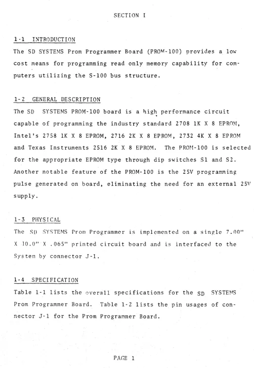
1-4 SPECIFICATION
Table 1-1 lists the overall specifications for the SD SYSTEMS Prom Programmer Board. Table 1-2 lists the pin usages of con-nector J-1 for the Prom Programmer Board.
[image:4.621.55.570.48.792.2]TABLE 1-1
+8 to +lOV 300 rna maximum +16 to 18V 100 rna maximum -16 to l8V 60 rna maximum OgeratIng temJ)erature O°C to SO°C Interface levels TTL Compa t ib 1 e
Programming time 100 seconds max for 16,389 bl ts
TABLE 1-2
tpI~ \iO SIGNAL NAME DIRECTION DESCRIPTIO~
1,51 +8V to +lOV INPUT POWER
2 +16V to +20V INPUT POWER
100~SO , GND
179 , 80 ,81 , 31 ,30
29,82,83 AO-A7 INPUT ADDRESS BUS
136 , 35 ,88 , 89 , 38
39,40,90 DO-O to DO-7 INPUT DATA BUS OUT
9S,~4,41,42,91,
~F3l43 -- \)1-0 to DI-7 OUTPUT DATA BUS TN
PWH \vP ITE
'~ rDBIN DATA BUS IN
'46 SINP pnRT INPUT CYCLE
!45 SOUT INPUT PORT OUTPUT CYCLE
99 / Pf)C
INPUT POWER ON CLEAR
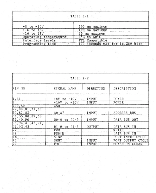
[image:5.617.13.559.50.725.2]2-1 INTRODUCTION
SECT[ON II
FUNCTIONAL DESCRIPTION
Functionally, the PROM Programmer consist of two main portions; hardware, and the software. The hardware allows the computer
to select the port bits, generate the programming pulse, and control the decoder. The software must direct the hardware in each of the operations described above. The major functions con-tained in the PROM Programmer hardware are shown in the block diagram (Figure 2-1).
2 - 2 DATA OUT BUS
The 8-Bit Data 0ut Bus is the S-lOO path for transferring data from the computer (CPU) to .the output ports on the Prom Program-mer board.
2-3· DATA IN BUS
The 8-Bit Data In Bus is the S-100 path for transferring data from the input port on the Prom Programmer Board to the computer
(CPU) .
2-4 AO-A7
The AD-A7 low order eight address lines are used by the computer (CPU) to select the various input/output ports through a decoder on the Prom Programmer Board.
2 - 5 I/O CONTROL LINES AND READ WRITE C0NTROL
The I/O Control Lines consist 0-£ PWlt, PD BIN, SINP and SOUTo
These lines are used to control the input and output operations from/to the I/O ports on the board.
2-6 ADDRESS DECODER
The Address Decoder detects when a port address used by the Prom Programmer is present on
(AD-A7).
The output of the de-coder is used to gate read and write pulses to the I/O ports.2-7 OUTPUT PORT 68H
Output port 68H is an 8 bit data register that transfers the data from CPU to ROM.
2~8 OUTPUT PORT 69H
Output port 69H is an 8 bit address register that determines the
1 ocat ion in the ROtvf for the da ta to he pro gramrned 0 r read.
2-9 OUTPUT PORT 6AH
Output port 6AH is an 8 bit control register with several control functions.
1. Bit 1 & 2
2. Bit 3 3. Bit 4 4. Bit 6
S. Bit 7 6. Bit 8
Two high order address bits A8
&
A9 address input3. One high order bit AID (address input for 2716).One high order bit All (address input for 2732). Program pulse for 2716/58.
Drive MOS clock drive.
Controls port 68H chip select for 2716/58/08.
2-10 INPUT PORT 68 H
Input port 68H is used to read the present data in the ROM.
PROM-JOO
24 PIN ZIP DIP SOCKET
PROGRAMMING PULSE CIRCUITRY
8
DATA INPUT PORT
(68H)
8
DATA OUTPUT PORT
(68H)
' - - - . 8
I
J 1v
F 1 CaJRE 2-1
Af
8 I0000----'''1 7 I
. . . - . - ' - - - . ,
ADDRESS OUTPUT
PORT
(69H)
DATA OUT BUFFER'
..
CONTROL OUTPUT
PORT
(6AH)
3-1 INTRODUCTION
SECTION III CONTROL SOFTWARE
Certain sequences must be executed to ensure proper programming of the prom.
3- 2 2758/16/32 PROGRA\1MING
Initially, and after each erasure, all bits of the 2716 are in the "high" state. Data is introduced by selectively programming "O's" into the required locations. Although only "O's" \vill be programmed both "1'5" and O's" can be presented in the data word. The only way to change a "0" to a "1" is by ultraviolet light erasure.
The 2716 is in the programming mode when the VPP power supply is 25V and CS is at a low TTL level. The data to be programmed is applied 8 bits in parallel to the data output port. The levels required for the address and data inputs are TTL.
When the addresses and data are stable a 50 MSEC, active high, TTL program pulse is applied to the appropriate input pin on the EPROM.
A program pulse must be applied to each address location to be programmed. The user can program any location at any time
-either individually, sequentially, or at random. The program pulse has a maximum width of 55 MSEC.
A verify is performed on the program bits to determine that they are correctly proirammed. The verify may be performed with VPP
at 25V.
3 - 3 2 7 0 8 PRO GRAMM I N G
Initially and after each erasure all 8192 bits are in high state (output high). Information is introduced by selectively program-ming "0" into the desired bit location. A programmed "0" can be changed to a "1" by UV. erasure.
The circuit is set up for programming operation by raising the CS/WE input (pin 20) to +12V. The word address is selected in the same manner as in the read mode. Data to be programmed is presented 8 bits in parallel to the data output lines (DO o -D0 7) Logic levels for address and data lines and the supply voltages are the same as for the read mode.
After address and data set up, one program pulse per address is applied to the program input pin 18. One pass through an address is defined as a program loop. The number of loops (N) required is a function of the program pulse width (tpw) allowing to
. (N) X (tpw) ~ 100. tpw in MSEC.
The width of the program pulse is from 0.1 to lms. The number of loops (N) is from a minimum of 100 (tpw=lms) to greater than 1000 (tpw=O.l). There must be N successive loops through all 1024 addresses. It is not permitted to apply N program pulses to an address and then change to the next address to be programmed.
*The PROM Programmer writes data received from the host com-puter into the PROM as guided by the address/control outputs supplied by the driver software. Basically, the PROM Program-mer manipulates the data and the address/control inputs from the
computer so that the subject PROM receives proper data, address and control inputs. The PROM-IOO generates the programming pulse for the 2708 from the output of a step up switching vol-tage regulator provided on the board. The same pulse is used to provide VPP (25V) at pin 21 of 2716/58. This 25V is set up by the driver software of the PROM Programmer.
Driver software for PROM Programmer must meet three requirements. These are: loading the object modules (diskettes) into host
computer memory, reading a PROM into memory and programming a PROM. Wi th in the so ftware, the executi ve sys tern coo rdinates all three operations while each operation sequence is run by its respective routine. In regards to the PR0M Programmer, only the read and program sequences are significant because they in-volve specific address/control inputs to the PROM Programmer. The requirements imply that, in addition to allocating a memory buffer for the driver software, the host computer must also supply a 1, 2 or 4K byte memory buffer for the data module to be loaded, read, and programmed.
3-4 LOAD SEQUENCE
The load sequence must be able to load data into memory at any location regardless of the routine load address contained in the file. Once the number of bytes to be loaded has been
specified, the user may load and program a portion of the file and then return for the rest. For example, if a file to be programmed contains 4K bytes, the user could program 2K bytes into one 2716 PROM and then program the remaining 2K bytes of the module into a second PROM.
3-5 READ SEQUENCE
The read sequence is necessary in order to perform a PROM copy function. Since the PROM programmer contains only one 24 pin ZIP DIP socket, the master PROM must first be read into the lK, 2K or 4K memory buffer (2708, 58 or 2716/32) and then programmed into an erased PROM. The host computer should offer memory editing to allow modification of the memory buffer before programming the new PROM.
3-6 PROGRAMMING SEQUENCE
The programming sequence actually involves a three step process.
1. Verify that PROM is erased. 2. Program the PROM.
3. Verify that the PROM contains correct data.
The entire PROM is read to verify erasure, that each location contains FFH. If unerased locations are found, the details are output to the console.
The programming of the PROM involves outputting the data for each of the lK, 2K or 4K locations sequentially along with the \ PROM address and the SOms program pulse for 2758/16/32 or lms program pulse for 2708. After this programming attempt is
COM-plete, the entire PROM must be read and compared with the memory buffer. If any locations do not match, the address and data should be output
io
the console.3-7 CAUTION:
In order to prevent possible destruction of PROMS, PROMS must never be inserted in to the ZIP DIP socket on the PROH Programmer until the driver software is running. If the PROM is inserted prior to starting the driver software, the PROM may be subjected to a continuous program pulse which will destroy the PROM. For the same reason, the host computer must not be reset while the PROM is in the socket.
3 -8 USING THE PR()M PROGRAMMER
The driver software can be used to load object files from diskettes, .read object code from PROMS and program object code into PRO~S.
As the driver software starts, the console prints the start/options message. The sign-on portion of the message indicates that th~
PROM Programmer software is operative. The options portion con-sist of the first of three questions about which operations are
to be performed (load a file, read a PROM, and program a PROM), in that order. The user answers the questions by entering a Y (for Yes) or N (for No) at the end of each question. If a Y is entered the respective operation is performed after the necessary parameters aie entered.
3-9 LOADING AN OBJECT FILE DISK FILE ONLY
Prior to answering the first question: READY TO LOAD A FILE (YIN)?
the user sets up the object file by specifying the file name, when loading the PROM-IOO Software: A> PROM08 filename. Ext. When the user answers the question with a Y, the PROM Programmer software asks the user to enter two parameters (load start address and load size) by printing HEX LOAD address, #Bytes: The parameters must be separated by a comma or space and terminated with a carriage return. If no parameters are entered in front of the carriage return, the object file will be loaded into the RAM locations specified on the module. However, since the PROM Programmer driver software occupies the memory location 0100H through SFFH the object file must not
overlay these locations. This condition can be prevented by using the load address parameter which allows relocating the object data to any area of memory. The number of bytes parameter allows the loading of a limited number of bytes of the file into ~1 so that object file may be loaded and programmed in blocks. If the load size parameter is not entered, the entire module is loaded. If a period is entered before the end of the parameter, the software repeats
the request for parameters allowing the user to correct the parameter. When the load is complete the PRO~·I Programmer software asks: READY TO PROGRAM A PROM (Y IN)?o
3-10 READING A PROM
In the console printout - READY TO READ A PROr..f (YIN)? If a Y
is entered, the PROM Programmer software asks the user to enter three parameters (MEM start address, MEM end address, PRO~t start address) by printing MEMORY START, MEMORY END,PROH START:
The MEM start and END parameters specify the memory space into which the data is tobe read. The PROM START defines the first
PROM location to be read. The three parameters must be separated by a comma or space and terminated with a carriage return. I f a period is entered before the end of the parameter the software repeats the request for parameters allowing the user to correct the parameters. When the read is complete or when the user
answers the question: READY TO READ A PROM (YIN)? With an N, the PROM Programmer software asks: READY TO PROGRAH A PROM (Y IN)?
3-11 PROGRAMMING A PROM
When the user answers the question: READY TO PROGRAM A PROM (YIN)?
with a Y, the programmer software asks the user to enter three parameters MEM start address, MEM end address and PROM start address by printing MEMORY START, MEMORY END, PROM START: The HEMORY START and END parameters specify the memory space from which the data is to be programmed. The three parameters must be separated by a comma or space and terminated with a carriage r~turn.
If a period is entered before the end of the parameters, the software repeats its request for parameters allowing the user to correct the parameters.
The PROM Programmer software first verifies that the PROM is erased (contains FFH in all locations). If the PROM Programmer s.oftware finds unerased locations, it prillflts the first unerased location. To check for other unerased locations the user enters a carriage return after each unerased location printed. If the PROM contains unerased location, the PROM must be erased again before starting programming. If there are unerased locations, the user may attempt programming by entering C. If there are no unerased locations, programming begins automatically. During the programming sequence, the PROQ,RAMMING LED COHES ON and stays on
till the program ends. To stop programming during the sequence the user enters a period (.). The PROM Programmer software asks DO YOU WISH TO LOAD A MODULE (YIN)? when the programming sequence is complete, the PPOM Programmer reads the PROM to verify that the data has been programmed correctly. If the PROM Programmer soft-ware finds locations with BAD data, it prints the bad locations. To stop the error listing the user enters a period and the soft-ware returns to the start asking: READY TO LOAD
A
FILE (YIN)?If the PRO!'-'f contains bad locations it should be re-erased and re-programmed until it is correctly r;>rogrammed. lAThen programming is done the user can exit the PROM Programmet software by typing a period (.).
3 -12 CO PY I N GAP ROH
Copying a master PROM into a subj ect PROM requires only that the master PROM be read as described in paragraph 3-10 and the subject PROM be programmed as described in paragraph 3-11.
SECTION IV CONSTRUCTION
4~1 INTRODUCTION
The SD SYSTEMS PROM Programmer board is intended for those people who have had some prior experience with kit building and digital
electronics. If you do not fall into this category it is highly recommended that you find an experienced person to help you in assembly and checkout of the board. Appendix B shows the parts list for the SD SYSTEMS PROM Programmer board. Double check all parts against this parts list. If any differences are noted please contact SD SYSTEMS.
NOTE: General construction information assembly diagram and schematic diagram can be found in the appendices.
4-2 ASSEMBLY PROCEDURE (SEE APPENDIX C)
1. Install and solder the IC sockets in their proper locations. 8 Pin at U14
14 Pin at U2,U3,U5,U9,UIO,Ull 16 Pin at U4
20 Pin at U6,U7,U8,U12,U13
NOTE: DO NOT INSTALL SOCKETS AT LOCATIONS Sl and S2. 2. Install and solder the resistors as follows:
A. R8 220 Ohm ~W 5% (Red,Red,Brown)
B. R4 22.lK Ohm 1!8W 1% (Precision Resistor) C. R5 I Ohm ~W 5% (Brown,Black,Gold)
D. R6 270 Ohm ~W 5% (Red,Violet,Brown) E. R7 100 Ohm ~W 5% (Brown,Black,Brown) F. Fl,2,3 lK Ohm ~W 5% (Brown,Black,Red)
3. Install and solder diodes CRI with banded end as shown on the
PC board.
A. CRl 1N5803
B. CR2 Zener Diode lN75l -5V
4. Install and solder the capacitors as follows: A. C1-C3,C6-Cll,C14,C15 O.IMF Ceramic
B. C12,C16-C18, IOMF 20V Tantalum C. C13 .002MF Ceramic
D. C4 500MF 35V Dilectric Axial Leads E. C5 300pf
5. Install and solder the voltage regulators with the heatsinks 6106-14 using the #6-32 hardware supplies.
VR1 =5v 7805 or LM340T-5 VR2 +12V 7812 or LM340T-l2 6. Install and solder L1 coil.
L1 J12044 SOD Micro Henry
7. Install and solder dip switches Sl and S2.
8. Double check all solder connections for cold solder joints, unsoldered connections or shorted connections.
4-3 VOLTAGE CHECK
1. Install the board in the computer and measure the output of +5V regulator, +12V regulator and -5V of CRI respectively. A. VRI
=
+5V (Top Pin)B. VR2 = +12V (Bottom Pin) C. CR2
=
-5V (Anode)NOTE: Do not proceed with board checkout until all power supply voltages are correct. The TTL and MOS logic can be permanently damaged if improper voltages are applied.
2. Install the Ie's in their sockets observing the Pin I designation on each socket marked on the PC Board.
A. UI 24 Pin Zip Dip socket (Pin 1 lever in lower left.) B. UZ TL497ACN
C. U3 74LS30
D. U4 74L5l55
E. U6, U8 74L5Z73 F. US, UIO 74LSl4
G. U7 74LS373
H. U9 7406
I. Ull 74LS08 J. U12, 13 74LS244
K. U14 DS002SCN
3. Double check all IC's for proper orientation and location.
4. Refer the switch selection option and position then as described in Section V.
5-1 INTRODUCTION
SECTION V SWITCH SELECTION
PROM Programmer has been designed to accomodate a variety of PROMS. Care must be taken to select the right positions of the switches for the users specific PROM selection. Table 5-1 lists the proper switch positions for each PROM type.
PROM TYPE 51 S2
2708 ( ) IK x 8 All other 2708
2758 (5V) All other All other 2716 (5V) All other All other 2732 (5V) 2732 All other
Table 5-1
6-1 INTPObuCTICN
SECTION VI
CHECK OllT
This section will describe some basic checks that should be made on the PRO~I Programmer.
NOTE: It is assumed at this point that the voltage checks
described in Section 4 have been previously rrade. The fol1o~ing
checks require that the CPU board also be plugged into the bus.
6-2 I/O PORT WRITE/READ VER~FICATION
Using the monitor in the system or a short program. Write data to output port 68 and read it back. Verify that the data read back is the same as that was written. This can be done as
follows if using the monitor .
. 0 6A 80 (cr) - enable Port 68
.0 68 dd (cr) - output data (dd) to port 68 .1 68 (cr) - input from port 68
68 dd - Data Read should be identical to data output
6-1 INTRODUCTION
SECTION VII
SOFTWARE REQUIREMENTS
The SD Systems PROM-lOO Programming Board software is available on disk on Intel 2716 EPROM.
A listing of the software in EPROM is included in Appendix D, while the disk version is included on the disk. (.PRN extension)
The program in PROM must be moved to lOOH prior to execution.
PROM 08, the 2708 programming utility, is located in the first
IK section of the PROM (0-3FFH). PROM 16, the Intel 2758, 2716, 2732 programming utility is located in the latter lK section of the PROM (400H-7FFH).
APPENDIX A
9S DIO 'Ii
<;)4 Ci I
41 DI2
42 D 13,
~I D 14 '32 r'IS
~3 i)IG
43 017
UIO
77 PW1'l ~4 14lS'~ 4:; 50UT
I~ 74~5081 3
'2.
+5V C.I ;>NO
.I"'~
INPUT PORT
24 ___ 1,'1. GBH 12UI3~8L,..".~ _ _ _ _ _ _ _ _ _ _ _ _ _ _ ....,. _ _ _ _ -;~;;to ~~~
~74LS244 r---t-i~---_:I::il 002
I
=\~4-11
~ S 15 r---rt-rt;~-~1500S :! IE. OOG~g!
'---I-w-r--''<I 74LS244 17007
L-_ _ _ +-~9< r.:'I~-;:-;-::---,
~74LS2.44
3 17
L---+~~,9<~7~4-L5~2~44~----'
7'" POBI N >-_-.,. _ _ ---,~~5 UII Eo 13 U,10""'.o:..2 _ _ _ _ -, 46 51 NP 74LSO~ __
1,::1 5Z 79 eo 81 '31 30 29 6Z 6"3 36 35 86 89 38 39 40 90 +5
+ 16V ~M~B'2 V~2i---_-_--+'2 L-_ _ _ _ -I-I~ 7 '~nlN ~7~4L~5~Z~44~--~ 13
OUTPUT PORT
~.
18 2
~1o:7;,-4:-:LS""2-::-44:;--- (OAn.~8H 'tSV ;~~ GNP 16 f;;4~c::-:--::--- 20 10 L - - -ca----+--"'< 11,."lN 74L52,.:.4..:.4 _ _ _ _ _ _ _ _ _ --::";>
INC7~~ t;' ,I ~~ ~ IO~~ .IMF ~ r - - - 3 ; - J E
i2-L
C3 CI7 + 8 >-_L_"' ... 7_BO--,S VR I 1--+ _ _ -.1 _MF--+_IO_M_F+-_ +5
10~1~* Y Cl2f&
GNo>-___ ~l_.~JL __ ~--~~-~-~--GND
- 16Y >---J~~-~----~~--~---SV US 4 ~E
R8 ...:,!, Ie 1'1'0 ., riSH 5 6 87 74LS'373
RZ AO AI 1.2 A'3 A4 A5 1>06 A7 000
DO I
DO 2-003
00 4 DO 5
:::-_-=2:.::2..::::0.n.~¥'W::""' _ _ _ _ _ _ _ _ _ _ _ __t-"':t':' U4 "rll~
"
U7 _ _ ~ f~ ~G14L515S'Y2 " 68H 1\ "4~~'4 :~:~~ ~ ~~ 2.'1'0 9 8 I OC 1.!.1":l.---'-_ _ - - '
~~ ' - 74LSI4
=74LS~ U3 " +5V Cgl GNP
:::-_-:-:-::---:7.-::-'I~Z ___ .J~---~ (ADORE~~~ .IMF
2.4 PIN Z.IP SOCKET
~~74LS30
74LSIA,V 10,p 20 10
+5
r~. "'~~~244
: : : - - - " - - - i · I
::-I 741.S~44
~1"11 3
r":74CSZ44
4t.:f1E.
II~ -1'5~~
--> - - - + z i 74~5244
~'t L')S..,.'2.4_4+-_--'
>---~~-~1~3~ II 3 4 7 8 13 14 17 18 E 74L5273 U~ ~ 2. 5 6 ~ 12 15 16 19
~-+-_ _ _ ~8 1.0
~-+ _ _ _ ---,7:':-1A I
1>'--+ _ _ _ _ _ 6'"11.2
~-+----5~A3
e - - + - - - -4::iA4
~-+----3~AS
e--+---7l2
AID
12-+----.!.j1 "7
DO 6 : : : - - - + . . iSL:f12 '>7;;4~LS~2~4.::.4 +-__ -.J ( . j AI." DO 7
~ 74LSi44
>---~~-r~11~~~~9~---~
ED r
<&=DIGITI>oL LOGIC ZERO~
U~
UI4
050025
r---"'j
~ '7 R7
I~--V I 100.0..
~ Ie.
{7: ~
"I:-[>~ CI"3
.002 MF 10 II
'TO US-IG
L _____ .J --=-74 LSO ..
99 poe I ~5 '2. ; U~5~' 4t.."..-~--i RIO
74~S14 74L514 27011.
e. U9 5 RS LI
74LSOe. ~-t---' ryn. SOO~
114 I'}""~ +I2V
+5 G"~ TL4':l7A
Jt:-::f1,
't12V~1~56
(:4 1;4 ~s CRI
500 '42..' K • p~ I"S&>3 MF '"
-7
NOTES:.6':. CI>oPI>oCITORS C6, C7, CI4; CIS I.RE.I MF.
_nAil _0011 APPLICATION
OEsatlPTION MT£ APp,
APPENDIX B
SD Systems
P.O. Box 28810. Dellllll. Texea 75228 214-271-4St37
BILL OF MATERIALB
Tltl. : PL No. lev.
PR()~~-100 0100140 b ...
Dot • ... r~
S· \
4
~11tt'r"'
Qf)i5
~\,V/
SheetI
Of;L
,
It:'
Qty SO-PINV
Description Unit eolt ExteNion1 1 7010007 7406, U9
2 1 7010166 74LS08, U11
.... ...
.,
7010172 74LS14, US, U104 1 7010180 74LS30, U3
5 1 7010226 74LS155, U4
6 2 7010264 74LS244, U12, U13 7 2 7010276 74LS273, U6, U8
l.a.
1 7010304 74LS373, U7 1 7010353 DS0025CN, U1410 1 7010354 TL497ACN, U2
11 1 7060010 24 PIN ZIP DIP, U1
12 1 7030007 . 1 MF
e"
13 1 7030022 500MF 35V, C414 1 7030006 300 pf, C5
15 4 7030009 10 MF 20V, C12, C16-18
16 1 7030034 .002 MF Ceramic, C13
17 3 7020073 1K Ohm 1/4W 5%, R1-R3
18 1 7020175 22.1K Ohm, 1%, R4·
19 1 7020001 1 Ohm 1/4W 5%, R5
20 1 7020059 270 Ohm 1/4W 5%., R6
~ 1 7020177 220 Ohm 1/2W, 5%, R8 .,:" 1 7060003 16 Pin Socket, U4
23 1 7120001 L1 Inductor 500 uh
SD·Syatame
BILL OF MATEIRIALB
Tltl.:
'L
No.••••
PROM-I00 0100140
•
L\
Date ...
~I
\6c \
11
J~redl
fjj6
rolf
Sheet1.
Of:l-It::, Qty SO-PIN V Description Unit
eo.t
Extensioft25 1 7040014 IN5803, CRl
26 1 7050012 Dip Switch, Sl
27 1 7050013 Dip Switch, S2
28 6 7060002 14 Pin Socket U2. , 3) 5,,91
'°
t
IIv
29 5 7060005 20 Pin Socket UG) 7J 8, a'2, ; 13
30 1 7060001 8 Pin Socket U'4
31 1 7000014 PCB Prom-100 FAB #0100042
32 1 7160001 7805 VF\ \
I
33 1 7160003 7812 VR'Z.
34 2 7130005 Heatsink
-35 2 7130006 Screw 6-32x3/8
36 2 7130007 Nut 6-32
37 1 702.0049 f'E5' S,ORj 100 OHM, ~4 W, 5% ') R7
38 1 7180002 LEDI
39 tt) 7lliOO 4-5
., H\r=-
ca ...
C3) C6-CIO,CI4)C5APPENDIX C PROM-IOO
DESCRIPTION DArE APp,
SO SYSTEMS 6ARL"
PROM-IOO
PROJ EHaR ASSEMBLY DRAWING
2. DEGREASE SOARD.
NOTES: &. APPLY THERMAL COMPOUND P.N. 12-8 TO VRI (2.
APPENDIX D
PROM08 SO SYSTEMS Z80 ASSEMBLER PAGE 0001
ADOR CODE STMT SOURCE STATEMENT
0001 NAME PROM08
0002 •
,
0003
,
·
0004
·
,
2708 PROM PROGRAMMER CONTROL PROGRAM0005 ; SDOS ENVIRONMENT
0006
·
,
9/27/79 0007·
,
0008
·
,
VERSION 1.3 CP/M COM'PATIBLE 8/26/800009
·
,
0010 ;0011 ; SYSTEM EQUATES 0012 ;
0013
·
,
>0000 0014 EXIT EQU OH
>0100 0015 TBASE EQU 100H
·
,
BASE OF TRANSIENT AREA>0068 0016 DATA EQU 68B
,
·
DATA PORT>0069 0017 LADD EQU 69H ; LOW ADDRESS PORT
>006A 0018 HACTL EQU 6AH ; HIGH ADDRESS + CONTROL PORT
>0000 0019 RBOUT EQU 0
>0005 0020 FDOS EQU 5
>005C 0021 FCB EQU 5CH
>0080 0022 BUFFER EQU 80H
>OOOF 0023 OPEN EQU 15
>0010 0024 CLOSE EQU 16
>0014 0025 READ EQU 20
>OOlA 0026 SETDMA EQU 26
>0080 0027 NBYTES EQU 128
>0064 0028 LOOPS EQU 100
0029 ;
0030 ; 0031
,
·
0032,
·
0033 ; 0034 ;0035 PSECT ABS
0036
·
,
>0100 0037 ORG TBASE ; START AT 100H
0038 ; 0039 ; 0040
·
,
0041 ; PROGRAM PROM ENTRY POINT
0042
·
, 0043 ; 0044·
,
0100 319607 0045 PPG LD SP,SPVAL
0103 218602 0046 LD HL,MSG1
0106 CDA005, 0047 CALL PTXT
·
,
"PROM08 VERSION 1.3"·. 0109 1E80 0048 LD E,80H
010B CD4D02 0049 CALL CONIN
alOE FE31 0050 CP 31H
0110 3806 0051 JR C,SETDLY
0112 lEBF 0052 LD E,OBFH
0114 2802 0053 JR Z,SETDLY
0116 lEOO 0054 LD E,O
0118 7B' 0055 SETOLY: LD A,E
0119 328C06 0056 LD (DLAY) ,A
D1lC 3E80 0057 LD A,NBYTES
PROMO 8 SD SYSTEMS Z80 ASSEMBLER PAGE 0002
ADDR CODE STMT SOURCE STATEMENT
0121 AF 0059 XOR A
0122 329206 0060 LD (FOPEN) ,A
0125 319607 0061 PPGO LO SP,SPVAL
0128 AF 0062 XOR A I • CLEAR ACC
0129 D36A 0063 OUT (HACTL) ,A
012B CD910S 0064 CALL CRLF
O12E 21EB02 0065 LD HL,MSG2
0131 CDA005 0066 CALL PTXT
·
,
"READY TO LOAD A FILE ?"0134 210000 0067 LD HL,O
0137 228D06 0068 LD (SCRl),HL ;CLEAR BYTE COUNTER
013A CD2D02 0069 CALL YORN
013D D2FD03 0070 JP NC,READ2 ; IF NOT,CHK READ
0140 CD9105 0071 PPGOB CALL CRLF
0143 3A9206 0072 LD A, (FOPEN)
0146 B7 0073 OR A
0147 2015 0074 JR NZ,PPGOC-$
0149 OEOF 0075 LD C,OPEN
014B 115COO 0076 LD DE,FCB
014E CD0500 0077 CALL FDOS
0151 FEFF 0078 CP 255
0153 2009 0079 JR NZ,PPGOC-$
0155 218303 0080 LD HL,MSGI0
0158 CDA005 0081 CALL PTXT
015B C36602 0082 JP RENTRY
015E OE1A 0083 PPGOC LD C,SETDMA
0160 118000 0084 LD DE,BUFFER
0163 CD0500 0085 CALL FDOS
0166 210703 0086 LD HL,MSG3
0169 CDA005 0087 CALL PTXT
·
,
"HEX LOAD ADDRESS, # BYTES016C CD1806 0088 CALL SCAN ; COLLECT DATA
016F 3A9106 0089 LD A, (NXCHR)
0172 FE2E 0090 CP
, ,
.
0174 28CA 0091 JR Z,PPGOB-$
0176 21B603 0092 LD HL,MSG12
0179 CDA005 0093 CALL PTXT
017C 2A9606 0094 LD HL, (OPR1)
017F CD7E02 0095 CALL PADDR
0182 CD9105 0096 CALL CRLF
0185 COOD02 0097 CALL THDR
,
·
READ ADDR/#BYTES 1ST LINE0188 E5 0098 PUSH HL
0189 ED5B9606 0099 LD DE, (OPR1)
.
,
LOAD ADDRESS ENTERED018D 3A9006 0100 LD A, (OPCNT)
0190 A7 0101 AND A
0191 2804 0102 JR Z,PPGOA-$ ; IF NO OPR'S JUMP
0193 ED52 0103 SBC HL,DE ; COMPUTE OFFSET
0195 E5 0104 PUSH HL
0196 Dl 0105 POP DE ; OFFSET REG
0197 El 0106 PPGOA POP HL
0198 ED538F06 0107 LD (SCR3) ,DE ; SAVE OFFSET
019C 1803 0108 JR PPG2-$
019E CDOD02 0109 PPGl CALL THDR ; LOAD ADDR/# BYTES
OlAl ED5B8F06 0110 PPG2 LD DE, (SCR3)
01A5 B7 0111 OR A ; CLEAR CARRY
01A6 ED52 0112 SBC HL,DE ; SUBTRACT OFFSET
01A8 CD6405 0113 PPG3 CALL TWDG
,
·
READ A BYTEOIAB 77 0114 LD (HL) ,A
·
,
STORE ITOIAC 229406 0115 LD (LAST),HL
PROM08
ADOR COOE
OIBO 01B1 01B4 01B5 01B8 01B9 OIBB OIBE OlBF OICO 01C2 01C3 0lC6 0lC9 OICC OICO OIDO 0104 01D5 0lD6 0lD7 0109 OIOC OlDF 01E2 0lE5 0lE8 OIEB OlEE OIFl 01F4 01F7 01FA 01FD 0200 0203 0206 0208 020A 0200 0210 0212 0214 0215 0216 0219 021A 021C 021D 0220 0221 0224 0225 0228 0229 E5 2A8D06 23 228006 El IDED CD6405 AF 81 280B E5 2lCB03 CDA005 CD7E02 El 2A8D06 ED4B9806 2B OB A7 ED42 DA9E01 2lE803 CDA005 2A9406 CD7E02 CD9105 212303 CDA005 CD2D02 D26602 CD9105 214203 CDA005 CD1806 3A9106 FE2E 28ED C34C04 CD5A06 FE3A 20F9 AF 4F CD6405 A7 280D 47 CD6405 67 CD6405 6F CD6405 C9 Fl
STMT SOURCE STATEMENT
0117 0118 0119 0120 0121 0122 0123 0124 0125 0126 0127 0128 0129 0130 0131 0132 0133 0134 0135 0136 0137 0138 0139 0140 0141 0142 0143 0144 0145 0146 0147 0148 0149 0150 0151 0152 0153 0154 0155
0156 i
0157 ; 0158 0159 0160 0161 0162 0163 0164 0165 0166 0167 0168 0169 0170 0171 0172 0173 0174 PPG4 PPG10 PPG10A PPG11
.
,
THDR THDRI PUSH LD INC LD POP DJNZ CALL XOR ADD JR PUSH LD CALL CALL POP LD LD DEC DEC AND SBC JP LD CALL LO CALL CALL LD CALL CALL JP CALL LD CALL CALL LD CP JR JP CALL CP JR XOR LD CALL AND JR LD CALL LD CALL LD CALL RET POPSD SYSTEMS Z80 ASSEMBLER PAGE 0003'
HL
HL,(SCR1) BYTE COUNTER
HL
(SCR1) ,HL HL
PPG3-$ i READ ENTIRE LINE
TWDG READ CHECKSUM
A A,C Z,PPG4-$ HL HL,MSG13 PTXT
PADDR i CHECKSUM ERROR
HL
HL, (SCR1)
BC, (OPR2) ; # OF BYTES TO READ HL ; IF O,THEN FFFF
BC A HL,BC
C,PPGl ; IF MORE,JUMP
HL,MSG14 PTXT HL, (LAST) PADDR CRLF HL,MSG4
PTXT ; "READY TO PROG A PROM ?"
YORN
NC,RENTRY CRLF
HL,MSG5
PTXT ; "MEM START,MEM END,PROM START
SCAN A, (NXCHR)
' . ' ; IF ' . ' EXIT Z,PPG11-$
PROG
FREAD LOOK FOR ' : '
,
:.
NZ ,THDR-$
A ; CLEAR CHECKSUM
C,A TWDG
A ; IS RECORD LENGTH O?
Z,THDRI-$ B,A
TWDG ; GET FIRST BYTE OF ADDRESS
H,A
TWDG ; GET SECOND BYTE
L,A
TWDG ; GET RECORD TYPE
PROMoe
so
SYSTEMS zeo ASSEMBLER PAGE 0004ADOR CODE STMT SOURCE STATEMENT
022A C30C01 0175 JP PPG10
0176
·
,
0177 ;0220 C04002 0178 YaRN CALL ECHO
0230 4F 0179 LO C,A
0231 FE2E 0180 CP
, ,
.
0233 CA6602 0181 JP Z,RENTRY
0236 B7 0182 OR A
0237 FE4E 0183 CP 'N'
0239 C8 0184 RET Z
023A FE59 0185 CP 'Y'
023C 20EF 0186 JR NZ,YORN-$
023E 37 0187 SCF
023F C9 0188 RET
0189 ;
0190
·
,
0240 C5 0191 CONST PUSH BC
.
,
CALL SOOS CONSOLE STATUS0241 05 0192 PUSH DE
0242 E5 0193 PUSH HL
0243 OEOB 0194 LO C,OBH
0245 C00500 0195 CALL 5
0248 B7 0196 OR A
0249 E1 0197 POP HL
024A D1 0198 POP DE
024B Cl 0199 POP BC
024C C9 0200 RET
0201
·
,
)024D 0202 ECHO:
0240 C5 0203 CONIN PUSH BC
.
,
CALL SOOS CONSOLE INPUT024E D5 0204 PUSH DE
024F E5 0205 PUSH HL
0250 OE01 0206 LD C,l
0252 CD0500 0207 CALL 5
0255 E1 0208 POP HL
0256 D1 0209 POP DE
0257 C1 0210 POP BC
0258 C9 0211 . RET
0212
·
,
0259 05 0213 CONOUT: PUSH DE
025A C5 0214 PUSH BC
025B E5 0215 PUSH HL
025C 59 0216 LO E,C
025D OE02 0217 LO C,02
025F C00500 0218 CALL 5
0262 E1 0219 POP HL
0263 C1 0220 POP BC
0264 D1 0221 POP DE
0265 C9 0222 RET
0223 ;
0266 AF 0224 RENTRY XOR A
0267 D36A 0225 OUT (HACTL) ,A
0269 CD9105 0226 CALL CRLF
026C 3A9206 0227 LO A, (FOPEN)
026F B7 0228 OR A
0270 CAOOOO 0229 JP Z,EXIT
0273 OE10 0230 LD C,CLOSE
0275 115COO 0231 LO OE,FCB
PROMO 8 SD SYSTEMS Z80 ASSEMBLER PAGE 0005
ADDR CODE STMT SOURCE STATEMENT
027B C30000 0233 JP EXIT
0234 ;
0235
·
,
027E 7C 0236 PADDR LD A,H
027F CDAC05 0237 CALL PACC
0282 7D 0238 LD A,L
0283 C38505 0239 JP PASP
0240
·
,
0241,
•0242 ;
0286 50524F4D 0243 MSGI DEFM 'PROM-08 VERSION 1.3'
2D303820 56455253 494F4E20 312E33
0299 ODOAODOA 0244 DEFW OAODH,OAODH
0290 49532054 0245 DEFM 'IS THIS SYSTEM RUNNING 2.0, 2.5, OR 4.0
48495320 53595354 454D2052 554E4E49 4E472032 2E302C20 322E352C 204F5220 342E3020 4D485A3F
02C9 ODOA 0246 DEFW OAODH
02CB 28322E30 0247 DEFM '(2.0 - 0 , 2 . 5 - 1 , 4. 0 - 2) I
202D2030 202C2032 2E35202D 2031202C 20342E30 202D2032 29
02E8 OAOD 0248 DEFW ODOAH
02EA 03 0249 DEFB 03H
02EB 52454144 0250 MSG2 DEFM 'READY TO LOAD A FILE (yIN)?'
5920544F 204C4F41 44204120 46494C45 2028592F 4E293F
0306 03 0251 DEFB 03H
0307 48455820 0252 MSG3 DEFM 'HEX LOAD ADDRESS, i BYTES: I
4C4F4144 20414444 52455353 2C2·02320 42595445 533A20
0322 03 0253 DEFB 03H
0323 52454144 0254 MSG4 DEFM 'READY TO PROGRAM A PROM (yIN)?'
PROMO 8 SO SYSTEMS
zao
ASSEMBLER PAGE 0006ADDR CODE STMT SOURCE STATEMENT
20412050 524F4D20 28592F4E 293F
0341 03 0255 DEFB 03H
0342 4D454D4F 0256 MSG5 DEFM 'MEMORY START,MEMORY END,PROM START:
,
52592053 54415254 2C4D454D 4F525920 454E442C 50524F4D 20535441 52543A20
0366 03 0257 DEFB 03H
0367 52454144 0258 MSG6 DEFM 'READY TO READ A PROM (YIN)?'
5920544F 20524541 44204120 50524F4D 2028592F 4E293F
0382 03 0259 DEFB 03H
0383 46494C45 0260 MSGI0 DEFM 'FILE NOT FOUND'
204E4F54 20464F55 4E44
0391 03 0261 DEFB 03H
0392 41545445 0262 MSGl1 DEFM 'ATTEMPTING TO READ PAST END OF FILEi
4D505449 4E472054 4F205245 41442050 41535420 454E4420 4F462046 494C45
03B5 03 0263 DEFB 03H
03B6 4C4F4144 0264 MSG12 DEFM 'LOAD START ADDRESS= '
20535441 52542041 44445245 53533020
03CA 03 0265 DEFB 03H
03CB 43484543 0266 MSG13 DEFM 'CHECKSUM ERROR AT LOCATIONS
4B53554D 20455252 4F522041 54204C4F 43415449 4F4E5320
03E7 03 0267 DEFB 03H
03E8 4C4F4144 0268 MSG14 DEFM 'LOAD END ADDRESS= I
2020454E 44202041 44445245 53533020
PROMO 8 SO SYSTEMS Z80 ASSEMBLER PAGE 0007 ADDR CODE STMT SOURCE STATEMENT
0270 i
0271
·
,
0272·
,
0273·
,
0274
·
,
PROM READ SEQUENCE 0275·
,
0276 0277 i
03FD CD9105 0278 READ2 CALL CRLF
·
,
READ PROM INTO MEMORY 0400 216703 0279 LD HL,MSG60403 CDA005 0280 CALL PTXT
·
,
"READY TO READ (YIN)?" 0406 C02D02 0281 CALL YORN0409 D2E801 0282 JP NC,PPG10A ; NO, THEN PROGRAM 040C CD9105 0283 READO CALL CRLF
040F 214203 0284 LO HL,MSG5
0412 CDA005 0285 CALL PTXT
·
,
"MEM START,MEM END,PROM START0415 C01806 0286 CALL SCAN
·
,
INPUT PARAMETERS 0418 3A9106 0287 LD A, (NXCHR)041B FE2E 0288 CP
,
•,
041D 28ED 0289 JR Z,READO-$
041F 3E40 0290 LD A,40H
0421 D36A 0291 OUT (HACTL),A ; TURN ON PROM VOLTAGE 0423 2A9606 0292 LO HL, (OPRl) i MEM START ADDR
0426 ED5B9A06 0293 LO DE, (OPR3) ; PROM START ADDR 042A C01705 0294 READ 1 CALL PREAD ; READ A BYTE OF PROM 042D 77 0295 LO (HL) , A ; SAVE BYTE IN MEM 042E CD3904 0296 CALL ADCMP ; INC AODR & COMPARE
0431 20F7 0297 JR NZ,READl-$ i IF NOT END,THEN JUMP
0433 AF 0298 XOR A
0434 D36A 0299 OUT (HACTL),A
0436 C3E801 0300 JP PPG10A ; WHEN COMPLETE, RETURN 0301
·
I0302
·
,
0303 0304 i0305
·
,
INC HL & OE THEN COMPARE HL WITH (IX) 0306·
,
EXIT WITH ZERO FLAG SET IF EQUAL0307 ;
0308 i
0439 13 0309 ADCMP INC DE ; INC PROM ADDR
043A 7A 0310 LD A~O
043B E607 0311 AND 7H ; MAX PROM ADOR=7FF
0430 57 0312 LO D,A
043E 23 0313 INC HL
043F 05 0314 PUSH DE
0440 E5 0315 PUSH HL
·
,
SAVE HL & OE0441 ED5B9806 0316 LD DE, (OPR2) ; GET RAM END ADDR
0445 13 0317 INC DE
0446 A7 0318 AND A
0447 ED52 0319 SBC HL,DE ; COMPARE
0449 El 0320 POP HL
044A Dl 0321 POP DE
044B C9 0322 RET
0323
·
,
0324 ;0325 ;
0326
·
,
PROMO 8
ADDR CODE
044C 044F 0453 0456 045.8 045A 045D 045F 0461 0462 0465 0468 0469 046B 046E 0471 0472 0474 0476 0478 047A 047C 047E 0480 0483 0486 0488 048B 048F 0490 0492 0493 0496 0497 049A 049C 049F 04Al 04A3 04A6 04A8 04AA 04AC 04AE 04BO 04Bl 04B4 04B5 04B7 04BA 04BE 04Cl 04C2 04C4 04C7 04C9 2A9606 ED5B9A06 CD1705 FEFF 2007 CD3904 20F4 1822 E5 214505 CDA005 El DB68 CD2605 CD4D02 4F FE2E 2806 FE43 2809 l8DE 3EOO D36A C32501 CD9105 0665 2A9606 ED5B9A06 05 2818 C5 CDEE04 Cl CD4002 2807 CD4D02 FE2E 2843 CD3904 20EA 18DE 3EOO D36A 1614 AF CDOB05 15 20F9 2A9606 ED5B9A06 CD1705 BE 2007 CD3904 20F5 18Bl
STMT SOURCE STATEMENT
0328 ; 0329 ; 0330 PROG 0331
0332 PROGI 0333
0334
0335 PRGIA 0336
0337
0338 PROG2 0339 0340 0341 0342 0343 0344 0345 0346 0347 0348 0349 0350
0351 PRG2A 0352
0353
0354 PROG3 0355
0356 PROG4 0357
0358 0359
0360 PROG5 0361 0362 0363 0364 0365 0366 0367
0368 PROG5A 0369
0370
0371 PROG6 0372
0373
0374 PROG6B 0375
0376 0377
0378 PROG6A 0379
0380 PROG7 0381
0382
0383 PRG7A 0384 0385 LD LD CALL CP JR CALL JR JR PUSH LD CALL POP IN CALL CALL LD CP JR CP JR JR LD OUT JP CALL LD LD LD DEC JR PUSH CALL POP CALL JR CALL CP JR CALL JR JR LD OUT LD XOR CALL DEC JR LD LD CALL CP JR CALL JR JR
SD SYSTEMS Z80 ASSEMBLER PAGE 0008
HL,(OPRl) ; MEM START ADDRESS DE, (OPR3) ; PROM START ADDRESS PREAD ; READ A BYTE (PROM) OFFH ; CHECK FOR ERASED BYTES NZ,PROG2-$ ; IF NOT ERASED JUMP ADCMP ; INC ADDR & CHECK FOR END NZ,PROGl-$ ; LOOP UNTIL END
PROG3-$ ; GO PROGRAM PROM HL
HL,MSG7
PTXT ; "NOT ERASED" HL
A, (DATA)
PRTER ; PRINT BAD LOCATION ECHO ; READ FROM CONSOLE C,A
' . ' ; CHECK FOR PERIOD Z,PRG2A-$ ; EXIT
'c'
;
CHECK FOR 'C'Z,PROG3-$ ; CONTINUE IF
'c'
ENTERED PRGIA-$ ; IF NOT ,PRINT NEXT ERRORA,O
(HACTL) ,A PPGO
CRLF
B,LOOPS+l
HL,(OPRl) ; SET MEM START ADDR DE, (OPR3) ; SET PROM START ADDR B
Z,PROG6-$ BC
PPROG ; PROGRAM ONE BYTE BC
CONST
Z,PROG5A-$ CONIN
,
.
.
Z,PROG9-$
ADCMP ; INC ADDR & CHECK END NZ,PROG5-$ ; FINISH THIS LOOP PROG4-$
A,O
(HACTL),A; TURN OFF ALL CONTROL LINES D,20
A
DELAY D
NZ,PROG6B-$
HL,(OPRl) ; MEM START ADDR DE, (OPR3) ; PROM START ADDR PREAD ; READ PROM DATA
(HL)
NZ,PROG8-$ ; IF NOT MATCH,JUMP ADCMP ; CHECK FOR END
NZ,PROG7-$
PROM08
ADDR CODE
04CB F5
04CC E5
04CD 215205
04DO CDA005
04D3 EI
04D4 CD4002
04D7 2807
04D9 CD4D02
04DC FE2E
04DE 289C
04EO FI
04EI CD2605
04E4 laDE
04E6 215C05
04E9 CDA005
04EC 188E
04EE CD2205
04F1 7A
04F2 F680
04F4 D36A
04F6 7E
04F7 D368
04F9 7A
04FA F6CO
04FC 036A
04FE 3E01
0500 CDOB05
0503 7A
0504 F680
0506 E687
0508 D36A
OSOA C9
OSOE F5
050C 3A8C06
OSOF 47
0510 F1
0511 10FE
0513 3D
0514 20F5
0516 C9
0517 CD2205
051A 7A
051B E607
0510 036A
STMT SOURCE STATEMENT
PROG8 PROG8A PROG9 PUSH PUSH LD CALL POP CALL JR CALL CP JR POP CALL JR LD CALL JR
SD SYSTEMS Z80 ASSEMBLER PAGE 0009
AF HL
HL,MSG8 PTXT HL
; "BAD LOCATION"
CONST
Z,PROG8A-$ CONIN
,
,
.
Z,PRG2A-$ AF
PRTER ; PRI NT ERROR l-lE S SAG E PRG7A-$ ; PRINT ALL BAD LOCATIONS HL,MSG9
PTXT PRG2A-$
; ABORTED 0386 0387 0388 0389 0390 0~91 0392 0393 0394 0395 0396 0397 0398 0399 0400 0401 0402 ; 0403 ; 0404 ; 0405 ; 0406 ; 0407 0408 0409 0410 0411 0412 0413 0414 0415 0416 0417 0418 0419 0420 0421 0422 0423 0424 0425 0426 0427 0428 0429 0430 0431 0432 0433 ; 0434 ; 0435 ; 0436 ; 0437 ; 0438 ; 0439 0440 0441 0442 0443
PULSE ONE PROM LOCATION
; PPROG ; DELAY: DELAY1 CALL LD OR OUT LD OUT LD OR OUT LD CALL LD OR AND OUT RET PUSH LD LD POP OJNZ DEC JR RET PADD A,D 080H
; LATCH LSB OF ADDRESS
(HACTL) ,A
A,(HL) ; FETCH DATA
(DATA),A; OUTPUT DATA A,D
OCOH ; TURN ON PROG
(HACTL),A PULSE A,l DELAY A,D 080H
; 1 MILLISEC DELAY
087H ; PROG PULSE OFF
(HACTL) ,A
AF
A, (DLAY) B,A AF
DELAY1-$ A
NZ,DELAY-$
; 2.0 MHZ - 80H ; 2.5 MHZ - OBFH ; 4.0 MHZ - OOH
READ ONE LOCATION OF PROM
;
PREAD CALL
LD AND OUT PADD A,D 7
; LATCH LSB OF ADDRESS
PROMO 8 SD SYSTEMS Z80 ASSEMBLER PAGE 0010
ADDR CODE STMT SOURCE STATEMENT
051F DB68 0444 IN A, (DATA)
0521 C9 0445 RET
0446
·
,
0447,
•0448
·
,
LATCH LOWER 8 BITS OF PROM ADDRESS 0449·
,
0450 ;
0522 7B 0451 PADD LD A,E
0523 D369 0452 OUT (LADD) ,A
0525 C9 0453 RET
0454
·
,
0455 ;0456 ;
0457 ;
0458 ;
0459 ; PRINTS ADDR/BAD DATA/GOOD DATA
0460
·
,
OF ERROR LOCATION 0461·
,
0462
·
,
0526 47 0463 PRTER LD B,A
0527 7A 0464 LD A,D
0528 CDAC05 0465 CALL PACC ; PRINT MSB OF ADDR
052B 7B 0466 LD A,E
052C 'CDAC05 0467 CALL PACC
.
,
PRINT LSB OF ADDR052F OE20 0468 LD C,20H
0531 CD5902 0469 CALL CONOUT
0534 78 0470 LD A,B
0535 CDAC05 0471 CALL PACC
.
,
PRINT BAD DATA0538 OE20 0472 LD C,20H
053A CD5902 0473 CALL CONOUT
053D 7E 0474 LD A, (HL)
053E CDAC05 0475 CALL PACC PRINT GOOD DATA
0541 CD9105 0476 CALL CRLF
0544 C9 0477 RET
0478
·
, 0479·
,
0480·
, 0481·
,
0545 4E4F5420 0482 MSG7 DEFM 'NOT ERASED
45524153 45442020
0551 03 0483 DEFB 03H
0552 42414420 0484 MSG8 DEFM 'BAD LOC
4C4F4320 20
055B 03 0485 DEFB 03H
055C 41424F52 0486 MSG9 DEFM 'ABORTED'
544544
0563 03 0487 DEFB 03H
0488
·
,
0489 ;04'90 ;
0491
·
,
TWDG-READ AND CONVERT 2 DIGITS TO BINARY 0492·
,
0493 ;
0564 CD5A06 0494 TWDG CALL FREAD ; READ A CHAR, 1ST DIGIT
0567 CD7D05 0495 CALL ASBIN ; ASCII TO BINARY
PROMO 8 SO SYSTEMS Z80 ASSEMBLER PAGE 0011 ADDR CODE STMT SOURCE STATEMENT
056B 07 0497 RLCA
056C 07 0498 RLCA
0560 07 0499 RLCA
056E C5 0500 PUSH Be ; SAVE C REG (CKSM)
056F 4F 0501 LD C,A
·
,
SAVE 1ST DIGIT0570 CD5A06 0502 CALL FREAD
·
I 2ND DIGIT 0573 CD7D05 0503 CALL ASBIN0576 B1 0504 OR C
·
,
OR IN.MSB'S 0577 C1 0505 POP BC·
,
RESTORE CKSM 0578 F5 0506 PUSH AF·
,
SAVE ACC0579 81 0507 ADD A,C •
,
ADD IN 2 DIGITS TO CKSM. 057A 4F 0508 LD C,A
057B Fl 0509 POP AF
·
,
RESTORE ACC057C C9 0510 RET
0511
·
,
0512·
,
0513·
,
0514·
,
0515
·
,
ASCII TO BINARY CONVERSION 0516 ;0517
·
,
057D 0630 0518 ASBIN SUB 030H
057F FEOA 0519 CP 10
0581 F8 0520 RET M
0582 0607 0521 SUB 7
0584 C9 0522 RET
0523 ;
0524 ;
PROMO 8 SD SYSTEMS Z80 ASSEMBLER PAGE 0012
ADDR CODE STMT SOURCE STATEMENT
0529
·
I0530 ;
0585 CS 0531 PASP PUSH BC
0586 CDAC05 0532 CALL PACC
0589 CD9B05 0533 CALL SPACE
058C CD9105 0534 CALL CRLF
058F C1 0535 POP BC
0590 C9 0536 RET
0537
·
I0538 0539 i
0591 OECD 0540 CRLF LD C,ODH
0593 C05902 0541 CALL CONOUT
0596 OEOA 0542 LD C,OAH
0598 C35902 0543 JP CONOUT
0544 ;
0545 ;
059B OE20 0546 SPACE LO C I I I
059D C35902 0547 JP CONOUT
0548 i
0549
·
,
0550 i0551 ;
0552
·
,
0553 ; PRINT TEXT 0554 ;
0555
·
,05AO 7E 0556 PTXT LO A, (HL) FETCH A BYTE
05Al FE03 0557 CP 3
05A3 C8 0558 RET Z
05A4 4F 0559 LO C,A
05A5 CD5902 0560 CALL CONOUT
05A8 23 0561 INC HL
05A9 C3A005 0562 JP PTXT
0563 ;
0564
·
I0565 ; PRINT ACCUMULATOR
0566 0567
,
·
05AC F5 0568 PACC PUSH AF
05AD OF 0569 RRCA
05AE OF 0570 RRCA
05AP OF 0571 RRCA
05BO OF 0572 RRCA
05B1 CDB505 0573 CALL PRVAL
05B4 Fl 0574 POP AF
0575 ;
0576 i
05B5 E60F 0577 PRVAL AND OFH
05B7 C690 0578 ADD A,90H
05B9 27 0579 DAA
05BA CE40 0580 ADC A,40H
05BC 27 0581 DAA
05BD 4F 0582 LD C,A
05BE C35902 0583 JP CONOUT
.
I PRINT ITPROMO 8
ADOR COOE
OSC1 OSC3 OSC6 OSC8 05CB 05CD 0500 0502 0505 0506 0507 0508 0509 05DA 05DC 05DD OSDF 05EO 05E2 05E5 05E7 05E8 05E9 05EC 05ED 05EE 05EF 05F2 OSF3 05F6 05F7 05F8' 05FB 05FC 05FF 0600 FE30 DAD70S FE3A DADS05 FE40 DAD70S FE47 D2D705 AF C9 AF 3C C9 FE20 C8 FE2C C8 FE2E CAE805 FEOD CO C5 CD9105 C1 AF C9 210000 45 CD4D02 4F 04 CDDA05 C8 CDC105 CO 79
SD SYSTEMS Z80 ASSEMBLER PAGE 0013 STMT SOURCE STATEMENT
0586 ; 0587 ; 0588 ; 0589 ; 0590 0591 0592 0593 0594 0595 0596 0597 0598 0599 0600 0601 0602 0603
0604 ;
0605 ; 0606 ; 0607 ; 0608 ; 0609 0610 0611 0612 0613 0614 0615 0616 0617 0618 0619 0620 0621 0622 0623 0624 ; 0625 ; 0626 ; 0627 ; 0628 ; 0629 ; 0630 ; 0631 ; 0632 ; 0633 0634 0635 0636 0637 0638 0639 0640 0641 0642 0643
CHECK FOR VALlO HEX CHARACTER
·
,
AORN AORNI AORN2 CP JP CP JP' CP JP CP JP XOR RET XOR INC RET, 0 '
C,AORN2 ; JUMP IF
<
30H '9'+1C,AORNI ; JUMP IF
<
3AH 'A'-1C,AORN2 ; JUMP IF
<
'A' 'F'+1NC,AORN2 ; JUMP IF
<
'G'A
A
A
; VALID DATA RET
; NOT HEX CHAR
CHECK FOR TERMINATOR
·
,
SPACE, COMMA, OR CARRIAGE RETURN
TERMCK CP RET CP RET CP JP CP RET PUSH CALL POP XOR RET
,
,
Z,
,
,
Z
.
,
.
Z,TCHKO ODH NZ
TCHKO BC
·
,
CRLF BC
A
SCAN FOR OPERAND FROM KEYBOARD
EXIT WITH DATA IN HL, AND TERMINATOR IN C. IF VALID DATA, RETURN WITH
ZERO FLAG SET. B CONTAINS # OF CHARACTERS ENTERED.
KEYIN LD LD CALL LD INC CALL RET CALL RET LD HL,O B,L ECHO C,A KEY1 B TERMCK Z AORN NZ A,C
; INC CHAR COUNT
; IF TERMINATOR, RETURN ; VALID DATA CHECK
PROMO 8
ADDR CODE
0601 CD7D05
0604 29"
0605 29
0606 29
0607 29
0608 85
0609 6F
060A C3F30S
060D OE3F
060F C05902
0612 3E2E
0614 329106
0617 C9
0618 AF
0619 219606
061C E5
0610 DOE1
061F 77
0620 010900
0623 119706
0626 EOBO
0628 329006
062B COEF05
062E C20006
0631 79
0632 329106
0635 FE20
0637 2806
0639 FE2C
063B 2802
0630 05
063E C8
063F DD7500
0642 007401
0645 3A9006
0648 3C
0649 329006
064C 0023
064E 0023
0650 79
0651 FE20
0653 2806
0655 FE2C
0657 2802
0659 C9
STMT SOURCE STATEMENT
; I NVCMO
.
,
CALL ADO ADD ADD ADD ADD LD JP LO CALL LO LO RETSO SYSTEMS Z80 ASSEMBLER PAGE 0014
ASBIN HL,HL HL,HL HL,HL HL,HL A,L L,A KEYI
C, '? I
CONOUT
A, I • I
; CONVERT TO BINARY
; SHIFT 4 BITS
(NXCHR),A
;SCAN -- SCANS THE OPERANDS INPUT FROM THE
; CONSOLE. THE OPERANDS ARE SAVED IN OPl,
0644 0645 0646 0647 0648 0649 0650 0651 0652 ; 0653 ; 0654 ; 0655 0656 0657 0658 0659 0660 0661 ;
0662 i
0663 ; 0664 0665 0666 0667 0668 0669 0670 0671 0672 0673 0674 0675 0676 0677 0678 0679 0680 0681 0682 0683 0684 0685 0686 0687 0688 0689 0690 0691 0692 0693 0694 0695 0696 0697 0698 0699 0700 0701 ;
; AS THE ARGUMENTS TO EXECUTE THEIR COMMANDS.
.
,
SCAN SCANI SCAN2 XOR LD PUSH POP LD LD LO LOIR LD CALL JP LD LO CP JR CP JR OEC RET LO LO LO INC LD INC INC LO CP JR CP JR RETA ;INITIALIZE
HL,OPRS ;CLEAR OPERANDS
HL
IX (HL) ,A
BC,9
;IX=POINTER TO OPERANDS
DE,OPRS+l
(OPCNT),A
KEYIN ; GET ONE OPERAND
NZ, INVCMD A,C
(NXCHR),A
I I
Z,SCAN2-$ I
,
IZ,SCAN2-$
B Z
(IX) , L
(IX+l),H
; IF NO DATA, RET
A, (OPCNT)
A
(OPCNT),A IX
IX
A,C
I I
; POINT TO NEXT OPR
Z,SCANl-$ I
,
IPROMO 8 SD SYSTEMS Z80 ASSEMBLER PAGE 0015 ADDR COOE STMT SOURCE STATEMENT
0702
·
,
0703·
,
065A E5 0704 FREAD PUSH HL
065B 05 0705 PUSH DE
065C C5 0706 PUSH BC
0650 3A9306 0707 LO A, (BCOUNT)
0660 FEBO 0708 CP NBYTES
0662 200C 0709 JR NZ,FREAD1-$
0664 OE14 0710 LD C,READ
0666 115COO 0711 LO OE,FCB
0669 CD0500 0712 CALL FOOS 1 LEAD FILE
066C B7 0713 OR A
0660 2011 0714 JR NZ,FERROR-$
066F AF 0715 XOR A
0670 218000 0716 FREAD 1 LD HL,BUFFER
0673 SF 0717 LD E,A
0674 3C 0718 INC A
0675 329306 0719 LD (BCOUNT),A
0678 1600 0720 LD 0,0
067A 19 0721 ADD HL,DE 1 POINT TO NEXT DATA
067B 7E 0722 LD A, (HL)
067C C1 0723 POP BC
067D D1 0724 POP DE
067E E1 0725 POP HL
067F C9 0726 RET
0680 C1 0727 FERROR POP BC
0681 D1 0728 POP OE
0682 E1 0729 POP HL
0683 219203 0730 LO HL,MSGll
0686 CDA005 0731 CALL PTXT 1 ATTEMPT TO READ PAST EOF
0689 C36602 0732 JP RENTRY 0733
·
,
)068C 0734 DLAY DEFS 1
)0680 0735 SCR1 DEFS 1 )068E 0736 SCR2 DEFS 1 )068F 0737 SCR3 DEFS 1 )0690 0738 OPCNT DEFS 1 )0691 0739 NXCHR DEFS 1 )0692 0740 FOPEN DEFS 1 )0693 0741 BCOUNT DEFS 1 )0694 0742 LAST DEFS 2 )0696 0743 OPRS DEFS 6 )0696 0744 OPR1 EQU OPRS )0698 0745 OPR2 EQU OPRS+2 )069A 0746 OPR3 EQU OPRS+4 )0796 0747 SPVAL EQU OPRS+100H
0748 i
0749 i
PROM08 SO SYSTEMS Z80 ASSEMBLER PAGE 0016
ADDR CODE STMT SOURCE STATEMENT
CROSS REFERENCE LISTING
SYMBOL VALUE TYPE STMT STATEMENT REFERENCES
---
---
---ADCMP 0439 0309 0383 0368 0335 0296
AORN 05Cl 0591 0641
AORNI 05D5 0599 0594
AORN2 05D7 0601 0598 0596 0592
ASBIN 057D 0518 0644 0503 0495
BCOUNT 0693 0741 0719 0707 0058
BUFFER 0080 0022 0716 0084
CLOSE 0010 0024 0230
CONIN 024D 0203 0393 0365 0049
CONOUT 0259 0213 0657 0583 0560 0547 0543 0541 0473 0469
CONST 0240 0191 0391 0363
CRLF 0591 0540 0620 0534 0476 0354 0283 0278 0226 0148
0143 0096 0071 0064
DATA 0068 0016 0444 0413 0342
DELAY 050B 0425 0431 0418 0375
DELAYI 0511 0429 0429
DLAY 068C 0734 0426 0056
ECHO 024D 0202 0636 0344 0178
EXIT 0000 0014 0233 0229
FCB 005C 0021 0711 0231 0076
FDOS 0005 0020 0712 0232 0085 0077
FERROR 0680 0727 0714
FOPEN 0692 0740 0227 0072 0060
FREAD 065A 0704 0502 0494 0159
FREADI 0670 0716 0709
HACTL 006A 0018 0443 0422 0416 0411 0372 0352 0299 0291
0225 0063
I NVCMD 060D 0656 0679
KEY1 05F3 0636 0651
KEYIN 05EF 0634 0678
LADD 0069 0017 0452
LAST 0694 0742 0141 0115
LOOPS 0064 0028 0355
MSG1 0286 0243 0046
MSG10 0383 0260 0080
MSGl1 0392 0262 0730
MSG12 03B6 0264 0092
MSG13 03CB 0266 0128
MSG14 03E8 0268 0139
MSG2 02EB 0250 0065
MSG3 0307 0252 0086
MSG4 0323 0254 0144
MSG5 0342 0256 0284 0149
MSG6 0367 0258 0279
MSG7 0545 0482 0339
MSG8 0552 0484 0388
MSG9 055C 0486 0399
NBYTES 0080 0027 0708 0057
NXCHR 0691 0739 0681 0659 0287 0152 0089
OPCNT 0690 0738 0692 0690 0677 0100
OPEN OOOF 0023 0075
OPRI 0696 0744 0378 0356 0.330 0292 0099 0094
PROMO 8 SO SYSTEMS Z80 ASSEMBLER PAGE 0017 ADOR CODE STMT SOURCE STATEMENT
OPR3 069A 0746 0379 0357 0331 0293
OPRS 0696 0743 0747 0746 0745 0744 0675 0670 PACC 05AC 0568 0532 0475 0471 0467 0465 0237
PADD 0522 0451 0440 0408
PADDR 027E 0236 0142 0130 0095
PASP 0585 0531 0239
PPG 0100 0045
PPGO 0125 0061 0353
PPGOA 0197 0106 0102
PPGOB 0140 0071 0091
PPGOC 015E 0083 0079 0074
PPG1 019E 0109 013S
PPG10 010C 0139 0175
PPG10A alES 0143 0300 0282
PPGl1 01F7 0148 0154
PPG2 01A1 0110 0108
PPG3 alAS 0113 0122
PPG4 01CO 0132 0126
PPROG 04EE 0408 0361
PREAD 0517 0440 0380 0332 0294
PRG1A 045A 0335 0350
PRG2A 047C 0351 0401 0395 0385 0347
PRG7A 04C4 0383 0398
PROG 044C 0330 0155
PROG1 0453 0332 0336
PROG2 0461 0338 0334
PROG3 0483 0354 0349 0337
PROG4 0488 0356 0370
PROG5 0492 0360 0369
PROG5A 04A3 0368 0364
PROG6 04AA 0371 0359
PROG6A 04B7 0378
PROG6B 04BO 0374 0377
PROG7 04BE 0380 0384
PROG8 04CB 0386 03-82
PROG8A 04EO 0396 0392
PROG9 04E6 0399 0367
PRTER 0526 0463 0397 0343
PRVAL 05B5 0577 0573
PTXT 05AO 0556 0731 0562 0400 0389 0340 0285 0280 0150 0145 0140 0129 0093 0087 0081 0066 0047
RBOUT 0000 0019
READ 0014 0025 0710
READ 0 040C 0283 0289
READ 1 042A- 0294 0297
READ 2 03FO 0278 0070
RENTRY 0266 0224 0732 0181 0147 0082
SCAN 0618 0669 0286 0151 0088
SCAN1 062B 0678 0699 0697
SCAN2 063F 0688 0685 0683
SCRI 0680 0735 0132 0120 0118 0068
SCR2 068E 0736
SCR3 068F 0737 0110 0107
SETDLY 0118 0055 0053 0051
SETOMA 001A 0026 0083
SPACE 059B 0546 0533
PROMO 8
ADDR CODE
TBASE 0100
TCHKO OSE8
TERMCR OSDA
THDR 020D
THDRI 0229
TWDG 0564
YORN 022D
ERRORS=OOOO
STMT SOURCE
0015 0619 0611 0159 0174 0494 0178
SD SYSTEMS Z80 ASSEMBLER PAGE 0018 STATEMENT
0037 0616 0639
0161 0109 0097
0166
0172 0170 0168 0164 0123 0113
PROM16 SO SYSTEMS ZSO ASSEMBLER PAGE 0001 AnDR CODE STMT SOURCE STATEMENT
0001 NAME PROM16 0002 i
0003 ,
0004
·
,
2716/2758 PROM· PROGRAMMER CONTROL PROGRAM 0005 SOOS ENVIRONMENT0006 9/27/79 0007
0008 •
,
VERSION 1.3 CP/M COMPATIBLE S/26/80 0009·
,
0010
0011
·
,
SYSTEM EQUATES 0012 ;0013 ;
>0000 0014 EXIT EQU OH
>0100 0015 TBASE EQU 100H i BASE OF TRANSIENT AREA >0068 0016 DATA EQU 6SH
·
,
DATA PORT>0069 0017 LAnD EQU 69H
·
,
LOW ADDRESS PORT>006A 0018 HACTL EQU 6AH
·
,
HIGH ADDRESS + CONTROL PORT >0000 0019 RBOUT EQU 0>0005 0020 FDOS EQU 5 >005C 0021 FCB EQU 5CH >OOSO 0022 BUFFER EQU SOH >OOOF 0023 OPEN EQU 15 >0010 0024 CLOSE EQU 16 >0014 0025 READ EQU 20 >OOlA 0026 SETDMA EQU 26 >OOSO 0027 NBYTES EQU 128 1>0064 0028 LOOPS EQU 100
0029
·
,
0030 i 0031·
,
0032·
,
0033,
·
0034 i0035 PSECT ABS 0036
·
,
>0100 0037 ORG TBASE ; START AT 100H 0038
·
,
0039
·
,
0040·
,
0041
·
,
PROGRAM PROM ENTRY POINT 0042 ;0043
·
,
0044 ;0100 31S507 0045 PPG LD SP,SPVAL 0103 218602 0046 LD HL,MSG1
0106 CD8F05 0047 CALL PTXT ; "PROM16 VERSION 1.3"
0109 1E25 0048 LD E,25H
010B CD4D02 0049 CALL CONIN
010E FE31 0050 CP 31H
0110 3806 0051 JR CySETDLY
0112 1E32 0052 LD E,32H
0114 2802 0053 JR Z,SETDLY
0116 1E4A 0054 LD E,4AH
0118 7B 0055 SETDLY: LD A,E
0119 327B06 0056 LD (DLAY) ,A
011C 3E80 0057 LD A,NBYTES
PROM16 SD SYSTEMS Z80 ASSEMBLER PAGE 0002 ADDR CODE STMT SOURCE STATEMENT
0121 AF 0059 XOR A
0122 328106 0060 LD (FOPEN) ,A
0125 318507 0061 PPGO LD SP,SPVAL
0128 AF 0062 XOR A ; CLEAR ACC
0129 D36A 0063 OUT (HACTL) ,A
012B CD800S 0064 CALL CRLF
O12E 21EB02 0065 LD HL,MSG2
0131 CD8F05 0066 CALL PTXT
,
·
"READYTO LOAD A
FILE ?"0134 210000 0067 LD HL,O
0137 227C06 0068 LD (SCRl) ,HL ;CLEAR BYTE COUNTER
013A CD2D02 0069 CALL YORN
013D D2FD03 0070 JP NC,READ2
.
,
IF NOT,CHK READ 0140 CD8005 0071 PPGOB CALL CRLF0143 3A8106 0072 LD A, (FOPEN)
0146 B7 0073 OR A
0147 2015 0074 JR NZ,PPGOC-$
0149 OEOF 0075 LD C,OPEN
014B 115COO 0076 LD DE,FCB
014E CD0500 0077 CALL FOOS
0151 FEFF 0078 CP 255
0153 2009 0079 JR NZ,PPGOC-$
015S 218303 0080 LD HL,MSGI0
0158 CD8F05 0081 CALL PTXT
015B C36602 0082 JP RENTRY
O15E OElA 0083 PPGOC LD C,SETDMA
0160 118000 0084 LD DE, BUFFER
0163 CD0500 0085 CALL FDOS
0166 210703 0086 LD HL,MSG3
0169 C08F05 0087 CALL PTXT ; "HEX LOAD ADDRESS, # BYTES
016C C00706 0088 CALL SCAN ;COLLECT DATA
016F 3A80