Accepted Manuscript
Effect of 60Co γ-ray irradiation on electrical properties of Ti/Au/GaAs1−xNx Schottky diodes
A. Teffahi, D. Hamri, A. Mostefa, A. Saidane, N. Al Saqri, J.F. Felix, M. Henini
PII: S1567-1739(16)30116-X
DOI: 10.1016/j.cap.2016.05.003
Reference: CAP 4227
To appear in: Current Applied Physics
Received Date: 4 March 2016 Revised Date: 14 April 2016 Accepted Date: 3 May 2016
Please cite this article as: A. Teffahi, D. Hamri, A. Mostefa, A. Saidane, N. Al Saqri, J.F. Felix, M. Henini, Effect of 60Co γ-ray irradiation on electrical properties of Ti/Au/GaAs1−xNx Schottky diodes, Current Applied Physics (2016), doi: 10.1016/j.cap.2016.05.003.
M
AN
US
CR
IP
T
AC
CE
PT
ED
Effect of
60Co
γ
-ray irradiation on electrical properties
of Ti/Au/GaAs
1-xN
xSchottky diodes
A.TEFFAHIa, D. HAMRIa, A. MOSTEFAa, A.SAIDANEa, N. Al Saqrib, c, J. F. Felixd, M.Heninib
a CaSiCCE Laboratory, ENP-Oran, B.P 1523 El M'Naouar, Oran 31000, Algeria bSchool of physics and Astronomy, Nottingham University , NG72RD, United Kingdom
c
Department of Physics, College of Science, Box 36, Sultan Qaboos University, Al Khoud 123, Oman d
Universidade de Brasília, Instituto de Física, Núcleo de Física Aplicada, Brasília, DF, 70910-900, Brazil.
aek1976@outlook.com
Abstract:
Current-voltage (I-V), capacitance-voltage-frequency (C-V-f) and conductance-voltage-frequency (G/ω-V-f) measurements at room temperature are used to study 50 kGy 60Co γ-ray electrical properties irradiation dependence of Ti/Au/GaAs1-xNx Schottky diodes with 0.2%; 0.4%; 0.8% and 1.2% nitrogen dilution. This γ-rayirradiation induces a permanent damage that has increased ideality factor and series resistance for all samples. It was accompanied by a decrease in Schottky barrier height with nitrogen content up to 0.4%N and remained constant thereafter. Radiation was also found to degrade the reverse leakage current. At high frequency (1 MHz), capacitance and conductance decreased after radiation due to a decrease in net doping concentration. Interface state density and series resistance were determined from C-V-f and G/ω-V-f characteristics using Hill-Coleman methods. Interface states density exponentially decreased with increasing frequency confirming the behavior of interface traps response to ac signal.
Series resistance increases after irradiation is attributed to carrier’s removal effect and mobility degradation. It has two peaks in the accumulation and inversion region for some diodes (0.4%N, 0.8%N). γ-ray irradiation produced traps levels and recombination centers that reduce relaxation time. An increase in %N content can impede irradiation damage with even some compensation when the percent of diluted nitrogen is high (1.2%N).
Keywords:
γ-ray irradiation; Schottky diode; Ideality factor; I–V, C–V-f , G/ω-V-f measurements
1. Introduction
M
AN
US
CR
IP
T
AC
CE
PT
ED
Tataroglu et al. [5], Belyaev et al. [6], Kataras et al. [7] have reported on the effect of γ radiation on the electrical properties of metal semiconductor (MS) and metal insulator
semiconductor (MIS) structures. They showed a reduction in barrier height and an increase in leakage current, ideality factor and series resistance. However, Bobby et al. [8] found a decrease in series resistance and in ideality factor for Au/n-GaAs γ irradiated diodes.
Recent experimental studies on particles irradiation effect on Ti/Au/GaAsN diodes have been undertaken by Shafi et al. [9] and Al Saqri et al. [10]. Shafi used Laplace Deep Level
Transient Spectroscopy (LDLTS) technique to investigate the effect of hydrogen irradiation on deep traps in GaAs1-xNx. They found that hydrogenation of as-grown GaAs1-xNx epilayers passivated most deep levels. However, for sample with 0.8%N concentration, hydrogen irradiation passivated some of the defects and reduced the concentration of others; it also created new defects. In the work of Al Saqri et al. [10], they investigated the effect of γ irradiation on the deep levels traps in GaAs1-xNx using I-V and LDLTS techniques. They found that for samples with N =0.2% - 0.4%, the number of traps decreased after irradiation, whereas for samples with N = 0.8% - 1.2 %, the number of traps remained the same. Ma et al [11] have shown that some traps states become inactive in DLTS measurement when the barrier height is less than 0.62eV, however such traps are active traps states under bias and have an impact on transport properties of the device that need to be investigated.
Hence, this paper reports on the effects of γ-ray irradiation on the electrical properties of GaAsN Schottky diodes using current-voltage (I-V), capacitance-voltage-frequency (C-V-f) and conductance-voltage-frequency (G/ω-V-f) measurements at room temperature. γ-ray irradiated devices have 0.2%, 0.4%, 0.8% and 1.2% N concentration contents. Parameters studied are ideality factor, series resistance, barrier height, relaxation time and interface states density. Cheung [12] and Hill-Coleman [13] methods are used to determine some of these parameters.
2. Experimental details
The Schottky diodes are made of an n-GaAs substrate on top of which is grown a 0.1 µm thick epitaxial buffer layer of GaAsN Si-doped (2.1018cm-3) followed by an epitaxial 1 µm thick active layer of GaAsN Si-doped (3.1016cm-3). At this stage, the wafers were ion irradiated at room temperature in a gamma cell Cobalt irradiator at a dose of 50 kGy with a dose rate of 5.143 kGy/h. Then devices are processed in the form of circular mesas with different diameters for electrical characterization. A Ge/Au/Ni/Au layer was evaporated and alloyed to form the Ohmic contact to the bottom of the n- GaAs substrate. Schottky contacts were formed by evaporation of Ti/Au on top of the doped epilayer.
Current-voltage (I–V) measurements were carried out using an Agilent precision
semiconductor parameters analyzer (4156C). The capacitance–voltage–frequency (C-V-f) and conductance –voltage–frequency (G-V-f) measurements were carried out with an Agilent LCR meter (4980A). The capacitance–frequency (C-f) and conductance–frequency (G-f) measurements were carried out with a Wayne Kerr Precision Impedance Analyzers (6500B).
3. Results and discussion
M
AN
US
CR
IP
T
AC
CE
PT
ED
All diodes show rectifying behavior at room temperature. Table 1 shows the rectifying ratio for
Ti/Au/GaAsN diodes at ±0.5 V. The rectifying ratio is found to be dependent on nitrogen content
and irradiation. This ratio decreased with increasing nitrogen content and irradiation. It is known that
nitrogen induce deep defects levels in band gap [9]. Irradiation is also known to induce defects in
the structure of devices and reduce rectifying behavior [6,10].
In diode with 1.2%N, the current quickly become dominated by series resistance. The series resistance is important in the down curvature of the forward bias. The trap levels reduce the free carrier density which in turn leads to an increase in the resistivity of the diode.
Reverse leakage current is the parameter that is most affected by γ-ray irradiation. As grown
samples have low leakage current compared to irradiated ones. Such increase has been attributed to the increase of generation recombination centers and image force barrier lowering [9, 14]. Reverse leakage current also exhibits strong dependence on the N concentration. Irradiated diodes with 0.4 % N content and 0.8% N content have non-saturating leakage current behavior as a function of bias and hence degrade rectifying properties of diodes. Here again interface defects are believed to be responsible for this behavior.
0.2%N 0.4%N 0.8%N 1.2%N
As grown 1.33 ×10⁷ 7×10⁵ 8.67×10⁵ 3.6×10⁴
irradiated 5.80 ×10⁵ 2.04×10³ 7.2×10³ 1.45×10³
Table 1: Rectifying ratio for Ti/Au/GaAsN Schottky diodes at ±0.5 V.
According to thermionic emission theory the current is given by [15]:
= . (exp( ( − /( − 1 (1
Where n is ideality factor, RS is series resistance, and I0 is saturation current given by:
= ∗ exp (− ∅/( (2
Where Aeff is the diode area (1.25x10⁻³cm2), k is the Boltzmann constant (1.381x10⁻²³ J/K), A*
is the modified Richardson constant (∗ = 4 ∗/ℎ! = 48.06/%&) with ∗ =
0.04 [16, 17]. A* is assumed constant after irradiation. T is the temperature in Kelvin. Using the method developed by Cheung [12]:
'(/'(() = ) + (/ (3
The ideality factor n can be obtained from the intercept on y-axis from Eq. (3) as:
= ( /(,/,(()
(4)
The extracted diodes parameters are summarized in Table 2. The value of ideality factor n varies from 1.08(1.12) to 1.41(1.51) after irradiation for 0.2%N(0.4%N) samples. The ideality factor value after irradiation is greater than 1 which indicates a contribution from
M
AN
US
CR
IP
T
AC
CE
PT
ED
The zero Bias barrier height (∅ ) can be obtained by Equation H(J) as
-() = − ( / (( )/(∗ (5 And
-() = ) + ∅/ (6)
The 0.2%N diode barrier height decreases after irradiation from 0.74eV before irradiation to 0.68eV after irradiation. As expected, the density of interface states was also affected by irradiation. It is known that gamma irradiation results in Fermi level pinning at defect level. However diodes with 0.8%N and 1.2%N concentration remain insensitive to irradiation. This is consistent with DLTS measurements observed by Al Saqri et al [10]. Whereas the Schottky barrier height increases with decreasing concentration [9].
parameters 0.2% N As-grown 0.2% N Irradiated 0.4% N As-grown 0.4% N Irradiated 0.8% N As-grown 0.8% N Irradiated 1.2% N As-grown 1.2% N Irradiated n-factor 1.08 1.41 1.12 1.51 1.05 1.37 1.11 1.46 series resistance(Ω) 0.68 1.07 0.75 1.81 1.95 0.98 25 106 barrier height (eV) 0.74 0.68 0.77 0.60 0.69 0.64 0.64 0.62
Table 2: Variation of n-factor, series resistance and barrier height with %N content and γ-radiation.
Figure (2) shows the variation of capacitance as a function of bias voltage for as grown and irradiated samples at different N content [0.2% - 1.2%]. A small ac signal with a frequency between 100 KHz and 1 MHz was added to dc bias to allow deep traps to capture and release electrons [13]. A capacitance curve has three regions corresponding to accumulation,
depletion and inversion. In accumulation region, the capacitance increase with decreasing frequency due to a continuous distribution of density of interface states (Nss) and series resistance [22].
The capacitance decreased after irradiation. This is attributed to a decrease in the (ND+NT) concentration and to a change in dielectric constant at the metal semiconductor interface after gamma irradiation [7, 23, 24]. The peak capacitance is lower for irradiated diodes. These peaks shift to the negative bias region due to a net positive charge at the interface [25-28]. A bump is observed close to the accumulation region when the bias is swiped from
accumulation to depletion. In depletion region the capacitance decreases with increasing reverse voltage for all devices. In inversion region, when the bias is highly negative, the density of activated deep traps (NT) start to contribute to the total electron density which change from (ND) to (ND+NT) [15].
From figure (3), the values of the conductance increase with increasing voltage for all
samples. However, its value decreases after gamma irradiation. This effect can be attributed to the decrease in the net ionized doping concentration, irradiation generates deep levels which trap conduction electrons and reduce the carrier concentration[26, 28, 29]. From Figure (3) the conductance decrease with increasing frequency due to capture and emission of carriers by interface states [13].
M
AN
US
CR
IP
T
AC
CE
PT
ED
1/0 = (2/( 1
23(4− (7
Where A is the diode area (1.25.10-3cm2), q is the electron charge, ND is the donor
concentration, Vi is the diffusion potential at zero bias, which is determined by the intercept
along voltage axis, εs is the static dielectric constant of GaAs (12.9εo). 1/C2– V plot shown in figure (4) is a straight line proportional to (ND)-1 indicating a uniform doping concentration for 0.2% and 0.4% N diodes. For higher negative bias non-uniform doping concentration for 0.8% N and 1.2%N indicates that there are a deep trap levels created by high N content and radiation damage. There slope is proportional to (ND+NT)-1 [15]. The barrier height was calculated from the relation:
6/ = 4 + (/ ln(19/12 − :ø/ (8)
Here NC is the effective density of states in conduction band for GaAs1-x-Nx at room temperature given by [31]:
1< = 2((2∗=>/ℎ!
(9)
The images Force barrier lowering and maximum electric field are given by:
∆∅/ = @( AB/(433 and AB = @2 12(4− / /(33 (10)
The values of barrier height, image force lowering and doping density are given in table 3. These values were extracted from C–V characteristics measured at high frequency (1 MHz), so to avoid interface state charges contribution [9, 10, 32]. We show a decrease in donor concentration for 0.2%N and 0.4%N diodes. Barrier heights extracted from C–V curves increase after gamma irradiation for 0.2%N, 0.4%N and 1.2%N diodes and are higher than those derived from I–V measurements. Such difference is explained by the presence of an interface layer or due to the barrier inhomogeneity [15, 19]. In other hand the extracted barrier heights for the 0.8% diode decrease from 0.82eV before irradiation to 0.74 after irradiation. The extracted parameters are not exact since the 1/C2–V plot is not linear. Several approaches have been used to overcome this problem. Among such methods that of Bryant et al [20] assumes a capacitance C0 in parallel with the depletion capacitance. The value of C0 can be found by plotting the measured capacitance as a function of V-1/2 and extrapolating the curve to the limiting value of C as V-1/2→0. The corrected capacitance is obtained by subtracting C0.Goodman et al[33] and Senechal et al [34] show that a plot dV/dC-2 against C gives a straight line with an intercept at C = 0 that gives the value ND+ NT, However. Such procedure it does not allow to extract the barrier height value.
parameters 0.2% N As-grown 0.2% N Irradiated 0.4% N As-grown 0.4% N Irradiated 0.8% N As-grown 0.8% N Irradiated 1.2% N As-grown 1.2% N Irradiated
[image:6.595.14.580.618.689.2]ND (cm-3) 6.09e+16 1.11e+16 5.99e+16 1.62e+15 1.63e+16 1.57e+17 1.08e+15 5.56e+15 image Force (eV) 0.0351 0.0236 0.0352 0.0159 0.0251 0.0452 0.0167 0.0198 barrier height(eV) 0.82 0.94 0.83 1.30 0.82 0.74 0.82 0.88
M
AN
US
CR
IP
T
AC
CE
PT
ED
Series resistance profiles can be obtained from the C–V–f and G/ω–V–f curves. To determine series resistance [7, 13, 35-38]:
= CB/(CB + (D0B (11)
where Cm and G m are the measured capacitance and conductance and ω=2πf is the angular
frequency.
Figure (5) shows the voltage-frequency dependency of the series resistance determined from equation (11). Notice that series resistance has a peak in forward bias for all diodes. Some of the irradiated samples (0.4%N and 0.8%N) show the presence of another peak in reverse bias. While the reverse bias peak shifts toward negative region, the forward peak shifts toward positive region. The magnitudes of these peaks decrease with increasing frequency. The frequency dependence of Rs is attributed to the particular distribution density of interface states [14, 28, 39]. The series resistance of all irradiated samples has increased .The increase of series resistance after radiation is attributed to the decrease of carriers’ mobility and carriers’ removal effect [40].
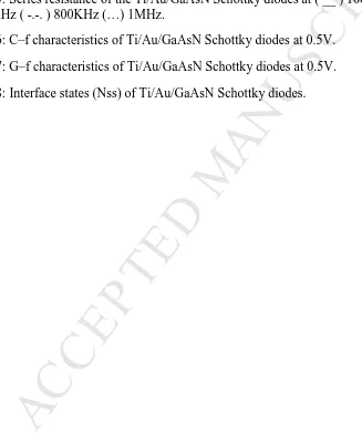
Figure (6) and figure (7) shows the variation of capacitance and conductance as a function of frequency for as grown and irradiated samples at different N content [0.2% - 1.2%] at 500mV bias. In lower frequency the capacitance is almost constant for all diodes, up to a certain frequency where it starts to drop to a lower constant value. The difference between these two values is due to the contribution of interface states that cannot follow the ac signal at high frequencies. The shift towards high frequency after gamma irradiation is due to a change in time constant of traps filling-empting. The conductance peak is an indication of the existence of interface states. The peak position shifts towards high frequency after gamma irradiation and to towards low frequency when N% is increased indicating a kind of composition effect. The relaxation time calculated from figure (7) decreases from 90µs to 17 µs for diodes with 0.2%N content, from 67µs to 42 µs for diodes with 0.4%N content, from 42 µs to 38 µs for diodes with 0.8%N content and from 21 µs to 12 µs for diodes with 1.2%N content.It can be noticed that the γ-ray irradiation decrease the relaxation time of all samples are in good agreement with results obtained by Tay et al [41]. This decrease is attributed to trapping and recombination centers produced by γ-ray irradiation [42].
An interface state is an allowed level within the forbidden gap. It is a donor type when it is above Fermi level and uncharged when it is below Fermi level. The density of interface states (Nss) as a function of frequency was extracted from C–V–f and G/ω–V–f characteristics. From Hill and Coleman method [13, 26, 27-32], the density of interface states (Nss) is given by:
1 = 2/( (CB/DBEF/(((CB/DBEF0GF+ (1 − 0
B/0GF (12
Where A is the diode area, ω is the angular frequency, Cma and Gma are the measured
capacitance and conductance which correspond to the peak values, respectively, and Cox is the
capacitance of the interfacial layer and it can be obtained from C–V and G/ω–V plots using [28]:
0GF = 0BEH1 + (CBE/(D0BEI (13
Many researchers [9, 43-46] have used DLTS, photoluminescence and
M
AN
US
CR
IP
T
AC
CE
PT
ED
The interface states profiles (Nss) before and after irradiation determined from equation (11) are given in figure (8). Density of traps shows an exponential decrease with frequency. This behavior is attributed to interface traps responding to the ac signal at low frequencies [17]. Gamma irradiation seems to have increased interface states for all diodes except that with 1.2%N. When computed at 100 KHz, interface states density has increased by
3.3×10¹³eV-1.cm-2 for diodes with 0.2%N content, by 6.74 × 10¹²eV-1.cm-2 for diodes with 0.4%N content and by 1.01×10¹²eV-1.cm-2 for diodes with 0.8%N content. Instead, it
decreased by 7×10¹⁰eV-1.cm-2 for diodes with 1.2%N content. One observes that an increase in %N content inhibits irradiation damage with even some compensation when the percent of diluted nitrogen is high (1.2%N) .The as grown diode (1.2%N) contain already a high
concentration of point defects that are believed to interact with the radiation-induced ones. This is also one of the reasons that the defects in irradiated diode are less than in as grown diode.
Irradiation is known [38, 47, 48] to induce displacement of the host atoms to form vacancies, interstitials, and antisite defects and annihilate others defects. Saqri et al [10] ,Auret et al [49- 50] andGoodman et al [51- 54] found that gamma rays,electron and alpha irradiation
enhance intrinsic defects like EL2 , which they assigned to arsenic antisite (AsGa ) or arsenic interstitial.
4. Conclusions
The room temperature electrical properties of Ti/Au/ GaAs1-xNx Schottky diodes have been characterized using I-V and C/G-V-f techniques. The investigated parameters are ideality factor (n), series resistance (Rs), barrier height (ΦB), doping concentration (ND) , relaxation time and density of interface states (Nss). Forward I–V measurements show that thermionic emission is the dominant transport mechanism. Ideality factor increased after irradiation due to recombination current and series resistance effects. However, Schottky diodes’ barrier decreased leading to a reverse saturation current increase. On the other hand, capacitance– voltage measurements at 1 MHz indicate that there is a slight decrease in carrier concentration and an increase in barrier height after irradiation. Discrepancies in barrier height between I–V measurements and C–V measurements are attributed to non linear behavior in 1/C2-V curves for samples with 0.8%N and 1.2%N due to deep trap effects.
C–V measurement, as a function of frequency, exhibits peaks that shift their position towards lower voltages with increasing frequency as their intensity decreases with increasing
frequency, this behavior is attributed to interface traps responding to the ac signal at low frequencies. The density of interface states and series resistance values has been obtained using Hill-Coleman method. The density of interface states distribution profile as a function of frequency increased after radiation due to irradiation-induced defect. The series resistance increase after irradiation and decrease with increasing frequency due to carrier’s removal effect and mobility degradation. γ-ray irradiation produce traps levels and recombination centers that reduce relaxation time.
The atoms’displacement damage was localized in different sample under test by extracting different parameters such as series resistance, barrier height and interface states density before and after irradiation. One observes that an increase in %N content inhibits irradiation damage with even some compensation when the percent of diluted nitrogen is high (1.2%N).
M
AN
US
CR
IP
T
AC
CE
PT
ED
[1] M. Kondow, T. Kitatani, S. Nakatsuka, M.C. Larson, K. Nakahara, Y. Yazawa, et al., GaInNAs: a novel
material for long-wavelength semiconductor lasers, IEEE Journal of Selected Topics in Quantum Electronics.
3 (1997) 719–730. doi:10.1109/2944.640627.
[2] S.-P. Han, H. Ko, J.-W. Park, N. Kim, Y.-J. Yoon, J.-H. Shin, et al., InGaAs Schottky barrier diode array
detector for a real-time compact terahertz line scanner, Optics Express. 21 (2013) 25874.
doi:10.1364/OE.21.025874.
[3] K. Ryczko, G. Sęk, J. Misiewicz, F. Langer, S. Höfling, M. Kamp, On the oscillator strength in dilute nitride
quantum wells on GaAs, Journal of Applied Physics. 111 (2012) 123503. doi:10.1063/1.4729320.
[4] P.C. Claeys, D.E. Simoen, Radiation Damage in GaAs, in: Radiation Effects in Advanced Semiconductor
Materials and Devices, Springer Berlin Heidelberg, 2002: pp. 109–144.
http://link.springer.com/chapter/10.1007/978-3-662-04974-7_4 (accessed February 27, 2016).
[5] A. Tataroğlu, Ş. Altındal, Gamma-ray irradiation effects on the interface states of MIS structures, Sensors and
Actuators A: Physical. 151 (2009) 168–172. doi:10.1016/j.sna.2009.02.035.
[6] A.A. Belyaev, R.V. Konakova, V.V. Milenin, J. Breza, T. Lalinsky, Radiation effects in surface-barrier
Ir-Al/n-GaAs structures, in: Second International Conference on Advanced Semiconductor Devices and
Microsystems, 1998. ASDAM ’98, 1998: pp. 231–234. doi:10.1109/ASDAM.1998.730206.
[7] Ş. Karataş, A. Türüt, Ş. Altındal, Effects of 60Co γ-ray irradiation on the electrical characteristics of
Au/n-GaAs (MS) structures, Nuclear Instruments and Methods in Physics Research Section A: Accelerators,
Spectrometers, Detectors and Associated Equipment. 555 (2005) 260–265. doi:10.1016/j.nima.2005.09.017.
[8] A. Bobby, N. Shiwakoti, S. Verma, P.S. Gupta, B.K. Antony, Enhancement in electrical properties of
Au/n-GaAs Schottky diodes exposed to 60Co gamma rays, Materials Science in Semiconductor Processing. 21
(2014) 116–121. doi:10.1016/j.mssp.2014.01.039.
[9] M. Shafi, R.H. Mari, A. Khatab, M. Henini, A. Polimeni, M. Capizzi, et al., Deep levels in H-irradiated
GaAs1-xNx (x < 0.01) grown by molecular beam epitaxy, Journal of Applied Physics. 110 (2011) 124508.
doi:10.1063/1.3664823.
[10]N. Al Saqri, J.F. Felix, M. Aziz, D. Jameel, C.I.L. de Araujo, H. Albalawi, et al., Investigation of the effects
of gamma radiation on the electrical properties of dilute GaAs1−xNx layers grown by Molecular Beam
Epitaxy, Current Applied Physics. 15 (2015) 1230–1237. doi:10.1016/j.cap.2015.07.010.
[11]Q.Y. Ma, M.T. Schmidt, X. Wu, H.L. Evans, E.S. Yang, Effect of Schottky barrier height on EL2
measurement by deep‐level transient spectroscopy, Journal of Applied Physics. 64 (1988) 2469–2472.
doi:10.1063/1.341655.
[12]S.K. Cheung, N.W. Cheung, Extraction of Schottky diode parameters from forward current‐voltage
characteristics, Applied Physics Letters. 49 (1986) 85–87. doi:10.1063/1.97359.
[13]W.A. Hill, C.C. Coleman, A single-frequency approximation for interface-state density determination,
Solid-State Electronics. 23 (1980) 987–993. doi:10.1016/0038-1101(80)90064-7.
[14]İ. Taşçıoğlu, H. Uslu, Ş. Altındal, P. Durmuş, İ. Dökme, T. Tunç, The effect of gamma irradiation on
electrical characteristics of Au/polyvinyl alcohol (Co, Zn-doped)/n-Si Schottky barrier diodes, J. Appl.
Polym. Sci. 118 (2010) 596–603. doi:10.1002/app.32450.
[15]E.H. Rhoderick, Metal-semiconductor contacts, IEE Proceedings I Solid State and Electron Devices. 129
(1982) 1. doi:10.1049/ip-i-1.1982.0001.
[16]W. Bachir Bouiadjra, M. amine Kadaoui, A. Saidane, M. Henini, M. Shafi, Influence of annealing
temperature on electrical characteristics of Ti/Au/GaAsN Schottky diode with 0.2% nitrogen incorporation,
M
AN
US
CR
IP
T
AC
CE
PT
ED
[17]W. Bachir Bouiadjra, A. Saidane, A. Mostefa, M. Henini, M. Shafi, Effect of nitrogen incorporation on
electrical properties of Ti/Au/GaAsN Schottky diodes, Superlattices and Microstructures. 71 (2014) 225–237.
doi:10.1016/j.spmi.2014.03.047.
[18]P. Jayavel, K. Asokan, D. Kanjilal, J. Kumar, Investigations on the annealing behavior of high-energy carbon
irradiated Au/n-GaAs Schottky barrier diodes, Materials Science in Semiconductor Processing. 3 (2000) 195–
199. doi:10.1016/S1369-8001(00)00032-9.
[19]M. Pattabi, S. Krishnan, Ganesh, X. Mathew, Effect of temperature and electron irradiation on the I–V
characteristics of Au/CdTe Schottky diodes, Solar Energy. 81 (2007) 111–116.
doi:10.1016/j.solener.2006.06.004.
[20]F.J. Bryant, J.M. Majid, C.G. Scott, D. Shaw, The interpretation of non-linear Schottky barrier C-2-V
characteristics, Solid State Communications. 63 (1987) 9–12. doi:10.1016/0038-1098(87)90055-X.
[21]S. Arulkumaran, J. Arokiaraj, N. Dharmarasu, J. Kumar, P. Magudapathy, K.G.M. Nair, Current-voltage
characteristics of low energy proton and alpha particle irradiated Au and Schottky barrier diodes, Solid-State
Electronics. 41 (1997) 802–805. doi:10.1016/S0038-1101(96)00102-5.
[22]A.F. Behle, R. Zuleeg, Fast neutron tolerance of GaAs JFET’s operating in the hot electron range, IEEE
Transactions on Electron Devices. 19 (1972) 993–995. doi:10.1109/T-ED.1972.17532.
[23]S. Demirezen, Z. Sönmez, U. Aydemir, Ş. Altındal, Effect of series resistance and interface states on the I–V,
C–V and G/ω–V characteristics in Au/Bi-doped polyvinyl alcohol (PVA)/n-Si Schottky barrier diodes at
room temperature, Current Applied Physics. 12 (2012) 266–272. doi:10.1016/j.cap.2011.06.016.
[24]M. Nishiguchi, T. Hashinaga, H. Nishizawa, H. Hayashi, N. Okazaki, M. Kitagawa, et al., Radiation tolerant
GaAs MESFET with a highly-doped thin active layer grown by OMVPE, IEEE Transactions on Nuclear
Science. 37 (1990) 2071–2075. doi:10.1109/23.101231.
[25]I. Dokme, S. Altindal, Comparative Analysis of Temperature-Dependent Electrical and Dielectric Properties
of an Schottky Device at Two Frequencies, IEEE Transactions on Electron Devices. 58 (2011) 4042–4048.
doi:10.1109/TED.2011.2165846
[26]Ş. Karataş, A. Türüt, Electrical properties of Sn/p-Si (MS) Schottky barrier diodes to be exposed to 60Co γ
-ray source, Nuclear Instruments and Methods in Physics Research Section A: Accelerators, Spectrometers,
Detectors and Associated Equipment. 566 (2006) 584–589. doi:10.1016/j.nima.2006.07.054.
[27]Z. Lin, Z. Yi-Men, Z. Yu-Ming, H. Chao, M. Yong-Ji, High energy electron radiation effect on Ni and
Ti/4H-SiC Schottky barrier diodes at room temperature, Chinese Phys. B. 18 (2009) 1931.
doi:10.1088/1674-1056/18/5/034.
[28]M.M. Bülbül, S. Zeyrek, Frequency dependent capacitance and conductance–voltage characteristics of
Al/Si3N4/p-Si(1 0 0) MIS diodes, Microelectronic Engineering. 83 (2006) 2522–2526.
doi:10.1016/j.mee.2006.06.002.
[29]E. Ayyildiz, Ç.N. Lu, A. Türüt, The determination of the interface-state density distribution from the
capacitance-frequency measurements in Au/n-Si schottky barrier diodes, Journal of Elec Materi. 31 (2002)
119–123. doi:10.1007/s11664-002-0157-9.
[30]Ö. Vural, Y. Şafak, A. Türüt, Ş. Altındal, Temperature dependent negative capacitance behavior of
Al/rhodamine-101/n-GaAs Schottky barrier diodes and Rs effects on the C–V and G/ω–V characteristics,
Journal of Alloys and Compounds. 513 (2012) 107–111. doi:10.1016/j.jallcom.2011.09.101.
[31]B. Akkal, Z. Benamara, B. Gruzza, L. Bideux, Characterization of interface states at Au/InSb/InP(100)
Schottky barrier diodes as a function of frequency, Vacuum. 57 (2000) 219–228.
doi:10.1016/S0042-207X(00)00131-7.
[32]Ş. Karataş, A. Türüt, Ş. Altındal, Irradiation effects on the C–V and G/ω–V characteristics of Sn/p-Si (MS)
M
AN
US
CR
IP
T
AC
CE
PT
ED
[33]A.M. Goodman, Metal—Semiconductor Barrier Height Measurement by the Differential Capacitance
Method—One Carrier System, Journal of Applied Physics. 34 (1963) 329–338. doi:10.1063/1.1702608
[34]R.R. Senechal, J. Basinski, Capacitance of Junctions on Gold‐Doped Silicon, Journal of Applied Physics. 39
(1968) 3723–3731. doi:10.1063/1.1656847.
[35]D. Korucu, A. Turut, R. Turan, Ş. Altindal, On the profile of frequency dependent interface states and series
resistance in Au/p-InP SBDs prepared with photolithography technique, Sci. China Phys. Mech. Astron. 55
(2012) 1604–1612. doi:10.1007/s11433-012-4761-2.
[36]Ç. Bilkan, A. Gümüş, Ş. Altındal, The source of negative capacitance and anomalous peak in the forward bias
capacitance-voltage in Cr/p-si Schottky barrier diodes (SBDs), Materials Science in Semiconductor
Processing. 39 (2015) 484–491. doi:10.1016/j.mssp.2015.05.044.
[37]E. Uğurel, Ş. Aydoğan, K. Şerifoğlu, A. Türüt, Effect of 6 MeV electron irradiation on electrical
characteristics of the Au/n-Si/Al Schottky diode, Microelectronic Engineering. 85 (2008) 2299–2303.
doi:10.1016/j.mee.2008.08.002.
[38]N. Tuğluoğlu, S. Karadeniz, Ö.F. Yüksel, H. Şafak, M. Kuş, 60Co gamma irradiation effects on the the
capacitance and conductance characteristics of Au/PMI/n-Si Schottky diodes, Indian J Phys. 89 (2015) 803–
810. doi:10.1007/s12648-015-0651-6.
[39]H. Uslu, M. Yıldırım, Ş. Altındal, P. Durmuş, The effect of gamma irradiation on electrical and dielectric
properties of organic-based Schottky barrier diodes (SBDs) at room temperature, Radiation Physics and
Chemistry. 81 (2012) 362–369. doi:10.1016/j.radphyschem.2011.12.029.
[40]M. Nishiguchi, T. Hashinaga, H. Nishizawa, H. Hayashi, N. Okazaki, M. Kitagawa, et al., Radiation tolerant
GaAs MESFET with a highly-doped thin active layer grown by OMVPE, IEEE Transactions on Nuclear
Science. 37 (1990) 2071–2075. doi:10.1109/23.101231.
[41]M. Tay, J. Gazecki, G. Reeves, Study of the effect of low energy electron irradiation on the density and
relaxation time of metal-insulator-GaAs interface states, Nuclear Instruments and Methods in Physics
Research Section B: Beam Interactions with Materials and Atoms. 65 (1992) 554–559.
doi:10.1016/0168-583X(92)95104-Y.
[42]H. Tecimer, H. Uslu, Z.A. Alahmed, F. Yakuphanoğlu, Ş. Altındal, On the frequency and voltage dependence
of admittance characteristics of Al/PTCDA/P-Si (MPS) type Schottky barrier diodes (SBDs), Composites
Part B: Engineering. 57 (2014) 25–30. doi:10.1016/j.compositesb.2013.09.040.
[43]Ł. Gelczuk, R. Kudrawiec, M. Henini, Identification of nitrogen- and host-related deep-level traps in n-type
GaNAs and their evolution upon annealing, Journal of Applied Physics. 116 (2014) 013705.
doi:10.1063/1.4886856.
[44]M.J. Legodi, F.D. Auret, S.A. Goodman, Electronic and transformation properties of a metastable defect
introduced in epitaxially grown sulfur doped n-GaAs by particle irradiation, Materials Science and
Engineering: B. 71 (2000) 96–99. doi:10.1016/S0921-5107(99)00356-6.
[45]M. Henini, B. Tuck, C.J. Paull, A microcomputer-based deep level transient spectroscopy (DLTS) system, J.
Phys. E: Sci. Instrum. 18 (1985) 926. doi:10.1088/0022-3735/18/11/010.
[46]M. Henini, B. Tuck, C.J. Paull, Deep states in GaAs LEC crystals, Solid-State Electronics. 29 (1986) 483–
488. doi:10.1016/0038-1101(86)90068-7.
[47]U. Tisch, E. Finkman, J. Salzman, The anomalous bandgap bowing in GaAsN, Applied Physics Letters. 81
(2002) 463–465. doi:10.1063/1.1494469.
[48]P. Sathyanarayana Bhat, A. Rao, G. Sanjeev, G. Usha, G.K. Priya, M. Sankaran, et al., Capacitance and
conductance studies on silicon solar cells subjected to 8 MeV electron irradiations, Radiation Physics and
M
AN
US
CR
IP
T
AC
CE
PT
ED
[49]F.D. AURET, S.A. GOODMAN, W.E. MEYER, R.M. ERASMUS, G. MYBURG, Deep Level Transient
Spectroscopy Characterization of Electron Irradiation Induced Hole Traps in p-GaAs Grown by Molecular
Beam Epitaxy, Japanese Journal of Applied Physics. Pt. 2, Letters. 32 (1993) L974–L977.
doi:10.1143/JJAP.32.L974.
[50]F.D. Auret, A. Wilson, S.A. Goodman, G. Myburg, W.E. Meyer, Electrical characteristics of neutron
irradiation induced defects in n-GaAs, Nuclear Instruments and Methods in Physics Research Section B:
Beam Interactions with Materials and Atoms. 90 (1994) 387–391. doi:10.1016/0168-583X(94)95577-8.
[51]S.A. Goodman, F.K. Koschnick, C. Weber, J.-M. Spaeth, F.D. Auret, Generation of EL2 defects by a 6-MeV
proton irradiation of semi-insulating GaAs, Solid State Communications. 110 (1999) 593–598.
doi:10.1016/S0038-1098(99)00151-9.
[52]S.A. Goodman, F.D. Auret, G. Myburg, Defect annealing of alpha-particle irradiated n-GaAs, Appl. Phys. A.
59 (1994) 305–310. doi:10.1007/BF00348235.
[53]S.A. Goodman, F.D. Auret, W.E. Meyer, The effect of alpha-particle and proton irradiation on the electrical
and defect properties of n-GaAs, Nuclear Instruments and Methods in Physics Research Section B: Beam
Interactions with Materials and Atoms. 90 (1994) 349–353. doi:10.1016/0168-583X(94)95569-7.
[54]S.A. Goodman, F.D. Auret, M. Hayes, G. Myburg, W.E. Meyer, Electrical and defect characterization of
n-Type GaAs irradiated with α-particles using a van de graaff accelerator and an Am-241 radio-nuclide source,
M
AN
US
CR
IP
T
AC
CE
PT
ED
Fig.1. I–V characteristics of Ti/Au/GaAsN Schottky diodes.
Fig. 2. C–V characteristics of Ti/Au/GaAsN Schottky diodes at ( __ ) 100KHz (---) 400KHz( -.-. (---) 800KHz (…(---) 1MHz.
Fig. 3. G/ω–V characteristics of Ti/Au/GaAsN Schottky diodes at ( __ ) 100KHz (---) 400KHz ( -.-. ) 800KHz (…) 1MHz.
Fig. 4: 1/C2–V characteristics of the Ti/Au/GaAsN Schottky diodes at ( __ ) 100KHz
(---) 400KHz ( -.-. ) 800 KHz (…) 1MHz.
Fig. 5: Series resistance of the Ti/Au/GaAsN Schottky diodes at ( __ ) 100KHz (---) 400KHz ( -.-. ) 800KHz (…) 1MHz.
Fig. 6: C–f characteristics of Ti/Au/GaAsN Schottky diodes at 0.5V.
[image:13.595.116.443.256.647.2]Fig. 7: G–f characteristics of Ti/Au/GaAsN Schottky diodes at 0.5V.