A Switched-Capacitor Bidirectional DC-DC Converter with
Wide Voltage Gain Range for Electric Vehicles with Hybrid
Energy Sources
Yun Zhang,
Member
,
IEEE
, Yongping Gao, Lei Zhou, and Mark Sumner,
Senior
Member
,
IEEE
Abstract—A switched-capacitor bidirectional DC-DC converter with a high step-up/step-down voltage gain is proposed for electric vehicles (EVs) with a hybrid energy source system (HESS). The converter presented has the advantages of being a simple circuit, a reduced number of components, a wide voltage-gain range, a low voltage stress, and a common ground. In addition, the synchronous rectifiers allow zero voltage switching (ZVS) turn-on and turn-off without requiring any extra hardware, and the efficiency of the converter is improved. A 300W prototype has been developed which validates the wide voltage-gain range of this converter using a variable low-voltage side (40V-100V) and to give a constant high-voltage side (300V). The maximum efficiency of the converter is 94.45% in step-down mode and 94.39% in step-up mode. The experimental results also validate the feasibility and the effectiveness of the proposed topology.
Index Terms—Bidirectional DC-DC converter, EVs, HESS, Switched-capacitor, Synchronous rectification, Wide voltage-gain range
I. INTRODUCTION
To address the challenges of fossil fuels as the primary
energy source for transport (including reducing stockpiles and polluting emissions) [1]-[2], electric vehicles (EVs) powered by battery systems with low or zero polluting emissions, are increasing in popularity. Although the developed advancement of batteries can provide higher population performance for EVs, the unlimited charging or discharging current (i.e. inrush current) from batteries will result in shorter battery cycle life, as well as reducing the efficiency [3]. The combination of a battery and super-capacitors as a hybrid energy source system (HESS) for electric vehicles is considered as a good way to improve overall vehicle efficiency and battery life [4]. Super-capacitors have advantages of high power density, high cycle life, and very good charge/discharge efficiency. They can also provide a large transient power virtually instantaneously and are therefore suitable for meeting sudden EV power changes such as acceleration or meeting an incline. The HESS
Manuscript received November 8, 2017; accepted December 22, 2017. This
work was supported in part by the National Natural Science Foundation of China under Grant 51577130, and in part by the Research Program of Application Foundation and Advanced Technology of Tianjin China under Grant 15JCQNJC03900.
Y. Zhang,Y. Gao, and L. Zhou are with the School of Electrical and Information Engineering, Tianjin University, Nankai, Tianjin, China (e-mail: zhangy@tju.edu.cn; gaoyongping@tju.edu.cn; Luxuszl@163.com).
M. Sumner is with the Department of Electrical and Electronic Engineering, University of Nottingham, Nottingham, England, U.K (e-mail: mark.sumner@nottingham.ac.uk).
can make full use of the performance of batteries and super-capacitors: the super-capacitors supply power for acceleration and regenerative braking with the battery meeting the requirement of high energy storage density for long range operation [5]. A challenge for the HESS is that the terminal voltage of super-capacitors is low, and varies over a wide range as they are charged or discharged. Therefore, a bidirectional DC–DC converter with a wide voltage-gain range is desired for the HESS to connect low-voltage super-capacitors with a high-voltage DC bus.
There are two broad classifications for bidirectional DC-DC converters, namely isolated converters and non-isolated converters. Isolated converters, such as half-bridge and full-bridge topologies are implemented using a transformer [6]-[8]. In addition, the half-bridge converter in [6] needs a center-tapped transformer which results in a complex structure, and the full-bridge converters in [7]-[8] require a higher number of semiconductor devices. High-frequency transformers and coupled inductors can be used in isolated converters to obtain high step-up and step-down ratios [9]-[11]. However, in [9], the realization of bidirectional power flow requires ten power semiconductors and two inductors. The converter in [10] requires two inductors in addition to the transformer, and three inductors are used for the converter in [11]. The structure of these converters is complex, the cost is high, and it is difficult to standardize the design. When the turns ratio of the high frequency transformer increases, the number of winding turns increase correspondingly and the leakage inductance of the transformer may result in high voltage spikes across the main semiconductors during switching transitions. In order to reduce the voltage stress caused by the leakage inductance, a bidirectional DC-DC converter with an active clamp circuit in [12] and a full bridge bidirectional DC-DC converter with a Flyback snubber circuit in [13] were proposed. Besides, the dual active bridge converter in [14] and the phase-shift full-bridge converter in [15] also utilized the leakage inductance to achieve the soft-switching, and the energies stored in the leakage inductance were transferred to the load. When the input and output voltages do not match the turns ratio of the transformer, the power switch losses will increase dramatically [16], which reduces the efficiency of the converter.
semiconductors make them unsuitable for application to EV HESS. The voltage gain of the bidirectional DC-DC converter in [19] is greatly improved, but the voltage stress across the power semiconductors is still equal to that of the high voltage side. The voltage stress across the power semiconductors of the bidirectional three-level DC-DC converters in [20] and [21] is half that of conventional buck-boost converters, but its voltage-gain range is still small. In addition, the low-voltage and high-voltage side grounds of this converter are connected by a power semiconductor, and therefore the potential difference between the two grounds is a high frequency PWM voltage, which may result in extra maintenance issues and EMI problems. The low-voltage and high-voltage sides of the bidirectional three-level DC-DC converter in [22] share a common ground, but the voltage-gain of this converter is still limited. In addition, this converter requires complicated control scheme to balance the flying-capacitor voltage. A high bidirectional voltage conversion ratio with lower voltage stresses across the power semiconductors can be achieved by the converter of [23] with a reasonable duty ratio, but the converter still has many problems such as a large number of components, and a high frequency PWM voltage between the low-voltage and high-voltage sides. The multi-level converter in [24] can achieve a high voltage gain with low voltage stress across the power semiconductors. However, this converter needs a higher number of power semiconductors which leads to increased losses and higher cost.
Switched-capacitor converter structures and control strategies are simple and easy to expand. They use different charging and discharging paths for the capacitors to transfer energy to either the low-voltage or the high-voltage side to achieve a high voltage gain. Thus, the switched-capacitor converter is considered to be an effective solution to interface the super-capacitors with the high voltage DC bus. Single capacitor bidirectional switched-capacitor converters were proposed in [25], [26], but the converter’s efficiency is low. The efficiency of the converter in [27] has been improved through soft-switching technology, but it required many extra components. [28] proposed a multi-level bidirectional converter with very low voltage stress across the power semiconductors, but twelve semiconductors are needed, and the drawbacks of low voltage gain, complex control and structure limit its application. The high voltage gain bidirectional DC-DC converters in [29], [30] need only four semiconductors. However, the maximum voltage stress of the converter in [29] is that of the high voltage side, and the maximum voltage stress of the converter in [30] is higher than that of the high voltage side, which will increase switching losses and reduce the conversion efficiency of these converters. The bidirectional converter in [31] only requires three semiconductors, but its voltage-gain range is still small. In addition, the low-voltage and high-voltage side grounds of this converter are connected by an inductor, which will also generate extra EMI problems. Finally, the converter in [32] has improved the conversion efficiency greatly, but it needs three inductors and a higher number of power semiconductors which increases the conduction losses and makes the design more challenging. Although exponential switched-capacitor converters have high step-up capabilities, they operate relatively poorly with respect
to the switch and capacitor voltage stresses, as they involve several different higher voltage levels [33].
To meet the requirements for the bidirectional converter for the super-capacitor in an EV HESS, a high ratio bidirectional DC-DC converter which uses synchronous rectification is proposed in this paper, as show in Fig. 1. The main contribution of the proposed converter lies in the integrated advantage of having a wide voltage-gain range, in the case of requiring less number of components with the reduced voltage stress. In addition, the synchronous rectifiers allow ZVS turn-on and turn-off without requiring any extra hardware. The efficiency of the power conversion is therefore improved, as well as the utilization of the power switches. Although the proposed converter has a high voltage gain, it is built without the magnetic coupling, and it can simplify the converter design due to eliminating the need for coupled-inductor. Finally, the proposed converter is suitable for EV applications because its input inductor can provide a continuous current, and the switched-capacitors can also be taken advantage of efficiently with the dynamic balanced switched-capacitor voltages.
The paper is organized as follows. In Section II, the topology of the switched-capacitor bidirectional DC-DC converter is presented. In Section III, the operating principles of the proposed converter are analyzed. The steady-state characteristics of the converter are analyzed in Section IV and experimental results are presented in Section V.
II. THE PROPOSED CONVERTER
Fig. 1 shows the proposed switched-capacitor bidirectional DC-DC converter which is composed of four power semiconductors Q1-Q4, four capacitors and one inductor L. Clow, and Chigh are the energy storage/filter capacitors of the low-voltage and high-voltage sides, and C1, C2 are the switched capacitors. L is an energy storage/filter inductor. In addition, power semiconductors Q2-Q4, and C1, C2, Chigh form the switched-capacitor network, including switched-capacitor units C1-Q2, C2-Q3 and Chigh-Q4. ilow, ihigh are the currents through the low-voltage and high-voltage sides, Ulow, UC1, UC2,
Uhigh are the voltages across Clow, C1, C2 and Chigh, respectively.
L
S1 Ulow Clow
-+
Q1
S2
Chigh
-+
Uhigh
Q2
S3
Q3
S4
Q4
- +
C1
C2
-+ Step-down
Step-up
ihigh
ilow
UC1
[image:2.612.340.538.521.621.2]UC2
Fig. 1 The proposed topology of the switched-capacitor bidirectional DC-DC converter.
III. OPERATING PRINCIPLES
(b) all the capacitances are large enough that each capacitor voltage is considered constant over each switching period. A. Step-Up Mode
When the energy flows from the low-voltage side to the high-voltage side, the output voltage Uhigh is stepped up from
Ulow by controlling the power semiconductor Q1, and the anti-parallel diodes of Q2, Q3 and Q4. UQ1, UQ2, UQ3 and UQ4 are the voltage stresses across the corresponding power switches in step-up mode. d1=dBoost is the duty cycle of Q1. Fig. 2 shows the typical waveforms in the step-up mode, and Fig. 3 shows the current-flow paths of the proposed converter.
t
0
0
t UQ1
t
0
t
t
0
0
t
0
UQ2
UQ3
UQ4
t0 ilow
Uhigh/2
Uhigh/2
Uhigh/2
Uhigh/2
t1 t2
[image:3.612.97.255.199.337.2]S1
Fig. 2 Typical waveforms of the proposed converter in step-up mode.
L
S1 Ulow Clow
-+
Q1
S2
Chigh
-+
Uhigh
Q2
Step-up
S3
Q3
S4
Q4
- +
C1
C2
-+
ihigh
ilow
UC1
UC2
-+uL
(a)
L
S1
Ulow Clow
-+
Q1
S2
Chigh
-+
Uhigh
Q2
Step-up
S3
Q3
S4
Q4
- +
C1
C2
-+
ihigh
ilow
UC1
UC2
-+uL
(b)
Fig. 3 Current-flow paths of the proposed converter in the step-up mode. (a) Mode I S1=1. (b) Mode II S1=0.
Mode I: Power semiconductor Q1 is turned on. The anti-parallel diode of Q3 turns on, while the anti-parallel diodes of Q2 and Q4 turn off. The current-flow paths of the proposed converter are shown in Fig. 2(a). The energy of the DC source
Ulow is transferred to inductor L. Meanwhile, C1 is being charged by capacitor C2. Chigh provides energy for the load.
Mode II: Power semiconductor Q1 and the anti-parallel diode of Q3 are off, while the anti-parallel diodes of Q2 and Q4
are on. The current-flow paths of the proposed converter are shown in Fig. 2(b). C2 charges from inductor L. Meanwhile, C1 is discharging and Chigh is charging. The DC source Ulow, L and
C1 provide energy for the load.
As shown in Fig. 2 and Fig. 3, when the proposed switched-capacitor bidirectional converter operates in the step-up mode, the currents flow into the corresponding anti-parallel diodes. This will result in lower efficiency, as well as lower utilization of the power semiconductors. Therefore, a high step-up/step-down ratio switched-capacitor bidirectional DC-DC converter with synchronous rectification is proposed further in this paper.
t
0
t0 t1 t2
S1
t S2
0
t S3
0
t S4
0
td td
td td
(a)
without current with current
during dead time L
S1 Ulow Clow
-+
Q1
S2
Chigh
-+
Uhigh
Q2
S3
Q3
S4
Q4
- +
C1
C2
-+ Step-up
ihigh
ilow
UC1
UC2
-+uL
(b)
Fig. 4 Synchronous rectification operating principle for the proposed bidirectional converter. (a) Gate signals and dead time in the step-up mode. (b) Current-flow paths in the step-up mode.
Fig. 4 shows the principle of operation of the synchronous rectification for the proposed switched-capacitor bidirectional DC-DC converter in the step-up mode. The power semiconductor Q1 switches according to the gate signal S1 shown in Fig. 4(a). During the dead time td, the current must flow in the corresponding anti-parallel diodes of Q2, Q3 and Q4, as shown in Fig. 4(b). Otherwise, the current will flow in the controlled power semiconductors Q2, Q3 and Q4 due to their lower on-state resistance and on-state voltage drop using the gate signals S2, S3 and S4 shown in Fig. 4(a). In addition, when
[image:3.612.332.544.200.457.2] [image:3.612.68.278.359.611.2]dead-time td, and then flow in the controlled MOSFETs of Q2,
Q3 and Q4 due to their lower on-state resistance, as shown in Fig. 4(b). As a result, the controlled MOSFETs of Q2, Q3 and
Q4 are also turned on with the ZVS. Thus, the efficiency of the converter can be further improved.
B. Step-Down Mode
When energy flows from the high-voltage side to the low-voltage side, the output voltage Ulowis stepped down from
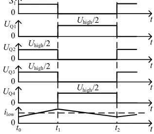
Uhigh by controlling the power semiconductors Q2, Q3 and Q4, and the anti-parallel diode of Q1. UQ1, UQ2, UQ3 and UQ4 are the voltage stresses across the corresponding power switches in step-down mode. The relationship between d2 and d4 can be written as d2=d4=dBuck, where d2 and d4 are the duty cycles of Q2 and Q4 respectively. Fig. 5 shows the typical waveforms in the step-down mode, and Fig. 6 shows the current-flow paths of the proposed converter.
0
t UQ1
t
0
t
t
0
0
t
0
UQ2
UQ3
UQ4
t0 ilow
Uhigh/2
Uhigh/2
Uhigh/2
Uhigh/2
t1 t2
t S2
0
t S3
0
S4
0
[image:4.612.336.546.52.317.2]t
Fig. 5 Typical waveforms of the proposed converter in step-down mode.
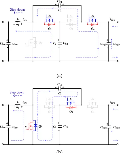
Mode I: Power semiconductors Q2 and Q4 are turned on. Power semiconductor Q3 and the anti-parallel diode of Q1 are off. The current-flow paths of the proposed converter are shown in Fig. 6(a). L is charging from capacitor C2. Meanwhile,
C1 is charging from Chigh and Uhigh. The DC source Uhigh, L and
C2 provide energy for the load.
Mode II: Power semiconductor Q3 and the anti-parallel diode of Q1 turn on, while power semiconductors Q2 and Q4 turn off. The current-flow paths of the proposed converter are shown in Fig. 6(b). L is discharging. Meanwhile, C2 is charging from capacitor C1, and Chigh is charging from Uhigh. L provides energy for the load.
Fig. 7 shows the synchronous rectification operating principle for the proposed switched-capacitor bidirectional DC-DC converter in the step-down mode. The power semiconductors Q2, Q3 and Q4 switch according to gate signals
S2, S3 and S4 shown in Fig. 7(a). During the dead time td, the current must flow in the corresponding anti-parallel diodes of
Q1, as shown in Fig. 7(b). Otherwise, the current can flow in the controlled power semiconductors Q1 due to its lower on-state resistance and on-state voltage drop using the gate signal S1 shown in Fig. 7(a). As a result, the controlled MOSFET of the synchronous rectifier Q1 is also turned on and turned off with ZVS.
L
S1
Ulow Clow
-+
Q1
S2
Chigh
-+
Uhigh
Q2
S3
Q3
S4
Q4
- +
C1
C2
-+
ihigh
ilow
UC1
UC2
+ -uL
Step-down
(a)
L
S1 Ulow Clow
-+
Q1
S2
Chigh
-+
Uhigh
Q2
S3
Q3
S4
Q4
- +
C1
C2
-+
ihigh
ilow
UC1
UC2
+ -uL
Step-down
(b)
Fig. 6 Current-flow paths of the proposed converter in the step-down mode. (a) Mode I S2S3S4=101. (b) Mode II S2S3S4=010.
t S2
0
t S3
0
S4
t
t1 t2
0
t S1
0
td td
t0
(a)
L
S1 Ulow Clow
-+
Q1
S2
Chigh
-+
Uhigh
Q2
S3
Q3
S4
Q4
- +
C1
C2
-+
ihigh
ilow
UC1
UC2
+ -uL
without current with current
during dead time
Step-down
(b)
Fig. 7 Synchronous rectification operation principle of the proposed bidirectional converter. (a) Gate signals and dead time in the step-down mode. (b) Current-flow paths in the step-down mode.
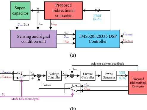
C. Control strategy of bidirectional power flow
Based on the operating principles previously described, the bidirectional power flow control strategy can be illustrated as shown in Fig. 8. The block diagram representation of the experimental configuration is shown in Fig. 8(a). The voltages
[image:4.612.105.251.256.434.2] [image:4.612.334.547.342.603.2]As shown in Fig. 8(b), the proposed bidirectional DC-DC converter switches between the step-up and the step-down modes, according to the power flow control signal Uc which is calculated by the TMS320F28335 DSP controller. It operates in the step-up mode when Uc=0, the voltage Uhigh is controlled by the voltage controller with the reference voltage Uref-Boost in the voltage-loop. Meanwhile, the feedback current ilow is controlled by the current controller using the reference current
Iref-Boost in the current-loop. The corresponding PWM schemes as shown in Fig. 2 and Fig. 4(a) are selected to generate the gate signals S1~S4 in the step-up mode.
In a similarly way, the converter operates in the step-down mode when Uc=1: the voltage Ulow is controlled by the voltage controller with the reference voltage Uref-Buck, and the feedback current ilow is controlled by the current controller with the reference current Iref-Buck, (which has the opposite polarity to the reference current Iref-Boost). The corresponding PWM schemes as shown in Fig. 5 and Fig. 7(b) are also selected to generate the gate signals S1~S4 in the step-down mode.
Proposed bidirectional
converter
Super-capacitor
Sensing and signal condition unit
ilow
TMS320F28335 DSP Controller Uhigh
Ulow(Usc)
Ulow Uhigh
ilow
PWM (S1-S4)
Uref-Buck
Uref-Boost
(a)
Uref Voltage
Controller Current Controller PWM Generator Proposed Bidirectional Converter
S1~S4 Inductor Current Feedback
Ulow Uhigh Iref Ufeedback ilow + - + -Uref-Buck Uref-Boost Uc
Mode Selection Signal
1
0 0
1
(b)
Fig. 8 Control strategy for bidirectional power flow. (a) Block diagram representation of experimental configuration. (b) Realization of double closed-loop control strategy.
IV. ANALYSIS OF STEADY-STATE CHARACTERISTICS
A. Voltage-gain in steady-state (1) Voltage-gain in step-up mode
As shown in Fig. 2 and Fig. 3(a), C1 and C2 are connected in parallel when S1=1, so that the voltages across C1 and C2 are equal. According to Fig. 3(a, b) and the volt-second balance principle on L, the following equations can be obtained:
Boost low Boost C2 low
C1 C2 high
C1 C2
(1 ) ( )
d U d U U
U U U
U U (1)
Therefore, by simplifying (1), the following equation can be written:
C1 C2 low
Boost high low Boost 1 1 2 1
U U U
d U U d (2)
Based on the law of energy conservation,
low low high high
I U U I . Therefore: low high Boost 2 1 I I d
(3)
where Ilow and Ihigh are the average currents of ilow and ihigh respectively in the step-up mode. According to (2), the voltage-gain of the proposed converter in the step-up mode is 2/(1-dBoost), which is twice as large as the voltage-gain of the conventional buck-boost converter. In addition, the voltage stress of C1 and C2 can be reduced to half of the output voltage
Uhigh.
(2) Voltage-gain in the step-down mode
As shown in Fig. 5 and Fig. 6(b), C1 and C2 are connected in parallel when S2S3S4=010, so that the voltages of C1 and C2 are equal. According to Fig. 6(a, b) and the volt-second balance principle on L, the following equation can be obtained:
Buck C2 low Buck low
C1 C2 high
C1 C2
( )=(1 )
=
d U U d U
U U U
U U (4)
Therefore, by simplifying (4), the following equation can be written:
C1 C2 high
Buck
low high
1 2
2
U U U
d U U (5)
By substituting IlowUlowUhighIhigh in (5):
Buck
high low
2
d
I I (6) where Ilow and Ihigh are the average currents of ilow and ihigh respectively in the step-down mode. According to (5), the voltage-gain of the proposed converter in the step-down mode is
dBuck/2, which is half of the voltage-gain of the conventional buck-boost converter. In addition, the voltage stress of C1 and C2 are still half of the input voltage Uhigh.
B. Voltage and current stresses of power semiconductors (1) Voltage stress
As shown in Fig. 3(a) in the step-up mode and Fig. 6(b) in the step-down mode, Q1 is turned on and Q2 is turned off, so that Q2 and C2 are connected in parallel. Therefore the voltages across Q2 and C2 are equal. Similarly, the voltages across the other power semiconductors can also be obtained. According to (2) in the step-up mode and (5) in the step-down mode, the voltage stress for the power semiconductors can be written as:
high
Q1 C2
high
Q2 Q3 C1
high
Q4 high C2
2 2 2 U U U U
U U U
U
U U U
(7)
[image:5.612.50.297.277.462.2]the voltage Uhigh. (2) Current stress
According to Fig. 3 and (3), the current stress of the power semiconductors in the step-up mode can be obtained by applying the ampere-second balance principle on C1, C2 and
Chigh as follows.
Q1 high
Boost Boost
Q2 Q4 high
Boost
Q3 high
Boost
2 1
( )
1
1 1 1
I I
d d
I I I
d
I I
d
(8)
In a similar way, according to Fig. 6 and (6), the current stress of the power semiconductors in the step-down mode can be obtained as (9)
Buck
Q1 low
Buck
Q2 Q4 low
Buck
Q3 low
Buck
1 2 1
1 2 2 1
d
I I
d
I I I
d
I I
d
(9)
Based on (8) and (9), it can be seen that the current stress of
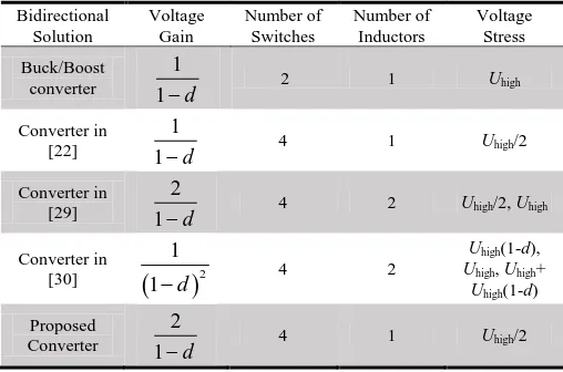
Q1 is slightly higher than that of the power semiconductors of a conventional buck-boost converter operating under the same conditions. However it is easier (and cheaper) to choose a MOSFET with a higher rated current than the one with a higher rated voltage. Furthermore, the proposed switched-capacitor bidirectional converter can obtain a high voltage gain while the duty cycle is in the range 0.5<dBoost<1 in the step-up mode or 0<dBuck<0.5 in the step-down mode. In addition, the voltage stress of all the power semiconductors is half of the high side voltage Uhigh, and the current stress of Q2, Q3 and Q4 is significantly lower than that of Q1 in both step-up and step-down modes. Therefore, the difference of the current stress is limited, and it will not affect the selection of the power semiconductors. Using these deductions comparisons can be drawn between the proposed topology and the other bidirectional solutions as shown in Table I.
The conventional buck-boost and the bidirectional DC-DC converter in [22] need one inductor respectively, but their ideal voltage-gain 1/(1-d) is limited to a lower value due to the effects of parasitic resistance and extreme duty cycles, and the lowest efficiency is less than 90%. It is noted that the voltage stress across the four semiconductors in the converter in [22] can be reduced by a half compared with that of the conventional converter, due to the use of two additional semiconductors and one flying capacitor. The high voltage-gain bidirectional DC-DC converters in [29] and [30] need two inductors respectively. In addition, in [29] , the maximum voltage stress across the semiconductors is the high side voltage Uhigh, and in [30] , the maximum voltage stress across the semiconductors is
Uhigh+ Uhigh(1-d). The converters in [29] and [30] both have semiconductors with a voltage stress higher than or equal to the
[image:6.612.118.232.136.220.2]high side voltage Uhigh, rather than Uhigh/2. For the converter proposed in this paper, the number of main components is between those of the converters described in [22] and [30] , the voltage stress across all the semiconductors is Uhigh/2, and its voltage gain is higher than that of [22] . When the step-up voltage gain is 6.25, the efficiency of the converter in [30] is approximately equal to 91.2%, while the proposed converter’s conversion efficiency is 91.9% with the same voltage gain. Moreover, the efficiency of the converter in [22] is nearly equal to 90% when Ulow=220V, Uhigh=340V, and Pn=300W, while the proposed converter’s efficiency reaches 94.39% when Ulow=100V, Uhigh=300V, and Pn=300W.
TABLE I
Comparisons between proposed and other bidirectional solutions.
Bidirectional Solution
Voltage Gain
Number of Switches
Number of Inductors
Voltage Stress
Buck/Boost converter
1
1d 2 1 Uhigh
Converter in [22]
1
1d 4 1 Uhigh/2
Converter in [29]
2
1d 4 2 Uhigh/2, Uhigh
Converter in
[30]
21
1d 4 2
Uhigh(1-d),
Uhigh, Uhigh+
Uhigh(1-d)
Proposed Converter
2
1d 4 1 Uhigh/2
V. EXPERIMENTALRESULTSANDAYALYSIS
[image:6.612.312.566.227.395.2]In order to validate the theoretical analysis, a 300W experimental prototype for the proposed switched-capacitor bidirectional DC-DC converter was developed, as shown in Fig. 9. The parameters of the experiment rig are shown in Table II.
TABLE II Experiment parameters.
Parameters Values
Rated power Pn 300W Storage/filter capacitors Clow and Chigh 520μF Switched-capacitors C1 and C2 520μF
Storage/filter inductor L 353μH
High side voltage Uhigh 300 V Low side voltage Ulow 40~100 V Switching frequency fs 20 kHz Power semiconductors Q1~Q4 IXTK 88N30P
[image:6.612.318.559.499.703.2]A. Experimental results in the step-up mode
In order to build the initial voltages across the switched capacitors and eliminate the inrush current when the converter starts up, a soft-starting circuit is adopted between the battery and the input side of the proposed converter in this paper. Then, the low voltage battery and the high voltage DC bus are interfaced by the proposed bidirectional DC-DC converter, and the experimental results are shown in Fig. 10. In Fig. 10(a), when the converter starts up, the input voltage Ulow rises from 0 to 50V gradually over 2 seconds, due to the soft-starting circuits. Accordingly, the output voltage rises from 0V to 300V (i.e. the reference voltage) gradually with a voltage control loop. It is noticed that the output voltage Uhigh arrives at the reference voltage (300V) before the input voltage Ulow reaches the battery voltage (50V), because the voltage control loop gets rid of the duty cycle limitation, and obtains the static state when the input voltage Ulow rises to 40V approximately. In addition, as shown in Fig. 10(b), the switched capacitor voltages UC1 and UC2 rise according to the output voltage Uhigh. It is also noticed that switched capacitor voltages UC1 and UC2 still keep at half of the output voltage Uhigh due to the voltage balance characteristic, especially in the soft start-up stage.
Ulow(20V/div)
Uhigh(100V/div)
t(400ms/div)
50V
300V
In soft start-up stage
(a)
UC2(50V/div)
UC1(50V/div)
t(400ms/div)
150V
150V
In soft start-up stage
[image:7.612.352.534.303.429.2](b)
Fig. 10 Experimental results of the soft start-up. (a) The input voltage Ulow and the output voltage Uhigh. (b) The voltages across C1 and C2.
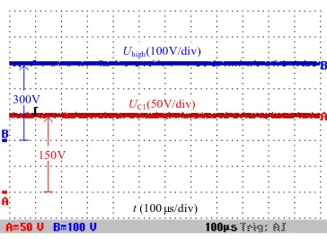
The voltage stress across the semiconductors and the capacitors in the step-up mode for Ulow=40V and Uhigh=300V are shown in Fig. 11 and Fig. 12. It can be seen in Fig. 11 that the duty cycle of the active power semiconductor Q1 is
dBoost=0.73, when the voltage-gain is 7.5. In addition, the PWM blocking voltage of each power semiconductor is 150V, namely half of the high-side voltage Uhigh, which validates the analysis in Section IV. The voltages across C1 and Chigh are
shown in Fig. 12. The voltage stress of C1 is 150V, which is also half of the high-side voltage Uhigh. Therefore, the switched-capacitor bidirectional DC-DC converter can perform with a high voltage-gain and a low voltage stress across the semiconductors and the capacitors.
The voltage waveforms of the synchronous rectifiers of the proposed converter in the step-up operating mode are shown in Fig. 13. The current flows through the anti-parallel diodes of Q2,
Q3 and Q4 during the dead time, and the blocking voltages of Q2,
Q3 and Q4 are around zero. Otherwise, the controlled MOSFETs Q2, Q3 and Q4 are turned on and turned off with ZVS by synchronous rectification. The gate signal S3 and the voltage stress of Q3 are shown in Fig. 13.
In the step-up mode, the output voltage stays constant around the reference voltage 300V by the action of the voltage control loop. Fig. 14 illustrates the dynamic state of the output voltage when the input voltage is changed from 100V to 40V over a period of 10s. According to Fig. 14, when the input voltage
Ulow varies from 100V to 40V, the output voltage remains at 300V, which means the proposed converter can obtain a wide voltage-gain range varying from 3 to 7.5.
UQ1(50V/div)
UQ2(50V/div)
d1≈ 0.73
d2≈ 0.27
t (10µs/div)
Fig. 11 The PWM voltages of power semiconductors Q1 and Q2.
UC1(50V/div)
Uhigh(100V/div)
t (100µs/div)
150V
[image:7.612.87.270.317.604.2]300V
Fig. 12 Voltages across C1 and Chigh under Ulow=40V and Uhigh=300V.
B. Experimental results in the step-down mode
The voltage stress of the semiconductors and the capacitors in the step-down mode for Ulow=40V and Uhigh=300V are shown in Fig. 15 and Fig. 16. It can be seen in Fig. 15 that the duty cycle of the active power semiconductor Q4 is dBoost=0.27, when the voltage-gain is 1/7.5. In addition, the PWM blocking voltage of each power semiconductor is 150V. The voltages across C2 and Chigh are shown in Fig. 16. The voltage stress of
[image:7.612.352.534.449.582.2]UQ3(50V/div) S3(5V/div)
ZVS Turn-off
ZVS Turn-on
t (4µs/div)
Fig. 13 Gate signal and voltage stress of synchronous rectification power semiconductor Q3.
Ulow(20V/div)
Uhigh(100V/div)
t (1s/div)
40V 100V
300V
Fig. 14 The output voltage and the wide-range changed input voltage from 100V to 40V in the step-up mode.
UQ3(50V/div)
UQ4(50V/div)
d3≈ 0.73
d4≈ 0.27
[image:8.612.87.269.51.178.2]t (10µs/div)
Fig. 15 The PWM voltages of power semiconductors Q3 and Q4.
UC2(50V/div)
Uhigh(100V/div)
t(100µs/div)
150V 300V
Fig. 16 Voltages across C2 and Chigh under Ulow=40V and Uhigh=300V.
Fig. 17 shows the voltage waveforms of the synchronous rectifier of the proposed converter in the step-down operating mode. The current flows through the anti-parallel diode of Q1 during the dead time, and the blocking voltage of Q1 is also close to zero. Otherwise, the controlled MOSFETs Q1 is turned
on and turned off with ZVS by synchronous rectification, as shown in Fig. 17.
Fig. 18 illustrates the dynamic state of the output voltage
Ulow and the input voltage Uhigh when the output voltage is controlled from 40V to 100V and the input voltage is kept at 300V. According to Fig. 18, under the control of the voltage loop, when the input voltage stays at 300V, the output voltage
Ulow can be controlled continuously over 8 seconds from 40V to 100V, which means the proposed converter can obtain a wide voltage-gain range varying from 1/7.5 to 1/3.
UQ1(50V/div)
S1(5V/div) ZVS
Turn-off
ZVS Turn-on
t(4µs/div)
Fig. 17 Gate signal and voltage stress of synchronous rectification power semiconductor Q1.
Ulow(20V/div) Uhigh(100V/div)
t (1s/div)
40V
[image:8.612.353.538.174.300.2]100V 300V
Fig. 18 The input voltage and the wide-range output voltage from 40V to 100V in the step-down mode.
C. Experiment results for bidirectional power flow control Fig. 19 shows the EV hybrid energy source system, where the super-capacitor bank is made up of CSDWELL model MODWJ001PM031Z2 super-capacitors. The battery in the HESS is a lithium iron phosphate battery, and a resistive load
[image:8.612.87.269.214.336.2] [image:8.612.351.536.334.459.2] [image:8.612.77.269.362.651.2]Super Capacitor
Battery
Motor BDC
Proposed BDC DC bus
Inverter Ibat
Ubat
Isc Usc
Psc Pbat
Pload
[image:9.612.56.279.50.146.2]M
Fig. 19 Hybrid energy sources system of electric vehicles.
The experimental results of the bidirectional power flow control are shown in Fig. 20. Fig. 20(a) shows Ibat and Isc when the proposed bidirectional DC-DC converter (BDC) is operating (i.e. the DC bus is powered by the HESS). Fig. 20(b) shows Ibat and Isc when the proposed BDC is not operating (i.e. the DC bus is just powered by the battery). It can be seen from Fig. 20(a) that, when the DC bus power demand is changed from 400W to 650W with a step change, the control system sets the control signal Uc=0. At the same time, the proposed switched-capacitor bidirectional converter responds quickly and operates in the step-up mode. The current Isc quickly goes to 6A, and the instantaneous power provided by the super-capacitor is nearly equal to the required power change of the DC bus, avoiding any step change in current from the battery. Following this process, the current of the battery rises from 8A to 13A gradually, and the current of the super-capacitor falls to zero from Isc=6A to match the increase of the battery current. Similarly, when the DC bus demand power is changed from 650W to 400W with a step change, the control system sets the control signal Uc=1. The proposed switched-capacitor bidirectional converter responds quickly and operates in the step-down mode. The current Isc quickly goes up to 6A with the opposite polarity. As a result, the current from the battery falls from 13A to 8A gradually, and the current of the super-capacitor falls to zero from Isc=-6A.
If the proposed BDC is not operating, the battery has to supply all the load demands by itself. It can be seen from Fig. 20(b) that, when the DC bus demand power is changed from 400W to 650W with a step change, the current Ibat needs to suddenly increase from 8A to 13A with a step change. When the DC bus demand power is changed from 650W to 400W with a step change, the current Ibat suddenly decreases from 13A to 8A with a step change. Therefore, when the load power changes with a step, the output current of the battery also has to change instantaneously. This has a detrimental impact on the battery itself during the electric vehicle’s acceleration and deceleration, as it shortens the battery’s service life.
Comparing the experimental results of Fig. 20 (a) and (b), it is seen that when the DC bus demand power suddenly increases or decreases, the proposed switched-capacitor bidirectional converter can respond quickly according to the control signal
Uc, and the super-capacitor can compensate (take in or send out) the power difference between the battery and the DC bus side to ensure that the current from the battery changes slowly. Therefore the overall aim of improving the battery life can be achieved.
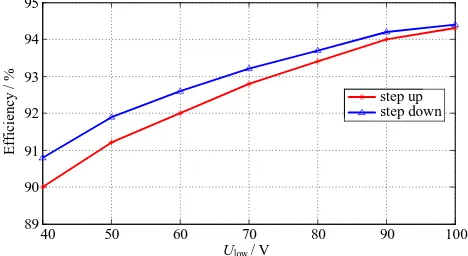
The efficiencies of the proposed bidirectional DC-DC converter in the step-up and step-down modes were measured
using a YOKOGAWA/WT3000 power analyzer and are shown in Fig. 21, when the high-side voltage Uhigh is 300V and the low-side voltage Ulow varies from 40V to 100V or 100V to 40V continuously. According to Fig. 21, the measured efficiencies range from 90.08 to 94.39% in the step-up mode, and from 90.86% to 94.45% in the step-down mode. The efficiencies are improved when the low-side voltage Ulow increases (due to the lower voltage-gain), and the efficiency in the step-down mode is slightly higher than that in the step-up mode. Moreover, the maximum efficiencies are 94.39% and 94.45% for step-up and step-down modes respectively when the low-voltage side Ulow is 100V.
Ibat (5A/div)
Isc (2A/div)
Sudden increase in load
Sudden decrease
in load
t (100ms/div) Boost
Buck
(a)
Ibat (5A/div)
Isc (2A/div)
Sudden increase in load
Sudden decrease
in load
t (100ms/div)
(b)
Fig. 20 Experimental results of bidirectional power flow control. (a) Super-capacitors are taken into operation. (b) Super-capacitors are not taken into operation.
40 50 60 70 80 90 100
89 90 91 92 93 94 95
step up step down
E
ffi
ci
en
cy
/
%
Ulow / V
Fig. 21 Efficiencies of the proposed switched-capacitor bidirectional converter in step-up and step-down modes (Uhigh=300V, Ulow=40V~100V, Pn=300W).
[image:9.612.347.531.198.485.2] [image:9.612.322.556.526.654.2]analyzing the power loss distributions, it can be concluded that the major loss comes from the inductor, namely the copper and core losses of the inductor account for 38.566% of the total losses. The capacitor losses account for 22.018% of the total losses. The conduction and switching (turning on and off) losses of the semiconductors account for 19.922% and 19.494%, respectively. In step-down mode, the total losses of the converter are 12.508W, and Fig. 22(b) shows the power loss distributions. The largest power losses are also the copper and core losses of the inductor, which account for 41.774% of the total losses. The conduction losses and the switching (turning on and off) losses of the semiconductors account for 39.422%, and the remaining 18.804% of the total losses is occupied by the capacitor losses.
Capacitor losses
Conduction losses
Copper losses
Core losses 1.85W 13.655% 3.375W
24.911% 2.641W 19.494%
2.699W 19.922%
Switching losses
2.983W 22.018%
(a)
Capacitor losses
Conduction losses
Copper losses
Core losses 1.85W 14.791% 3.375W
26.983% 2.484W 19.858%
2.447W 19.564% Switching losses
2.352W 18.804%
[image:10.612.76.272.219.439.2](b)
Fig. 22 Calculated power loss distributions for the experiment when Ulow=40V,
Uhigh=300V, and Pn=300W. (a) In step-up mode. (b) In step-down mode.
VI. CONCLUSIONS
A switched-capacitor bidirectional DC-DC converter has been proposed. The topology has a high step-up/step-down ratio and a wide voltage-gain range, in the case of requiring less number of components with the reduced voltage stress. The synchronous rectifiers can turn on and turn off using ZVS, and the efficiency is improved. The proposed bidirectional DC-DC converter, which interfaces the low voltage super-capacitor and the high voltage DC bus, can rapidly output or absorb the power difference due to a load step change. It can satisfy the requirements of a complex dynamic response, and effectively protect the battery from providing a step change in current. Thus, the proposed bidirectional DC-DC converter is suitable for the power interface between the low-voltage super-capacitors and the high-voltage DC bus of a HESS for electric vehicles.
REFERENCES
[1] A. Y. Saber, and G. K. Venayagamoorthy, “Efficient utilization of renewable energy sources by gridable vehicles in cyber-physical energy systems,” IEEE Syst. J., vol. 4, no. 3, pp. 285–294, Sep. 2010. [2] K. Sun, L. Zhang, Y. Xing, and J. M. Guerrero, “A distributed control
strategy based on DC bus signaling for modular photovoltaic generation
systems with battery energy storage,” IEEE Trans. Power Electron., vol. 26, no. 10, pp. 3032–3045, Oct. 2011.
[3] T. H. Pham, J. T. B. A. Kessels, P. P. J. van den Bosch, and R. G. M. Huisman, “Analytical solution to energy management guaranteeing battery life for hybrid trucks,” IEEE Trans. Veh. Technol., vol. 65, no. 10, pp. 7956–7971, Oct 2016.
[4] X. Liu, Q. Zhang, and C. Zhu, “Design of battery and ultracapacitor multiple energy storage in hybrid electric vehicle,” in Proc. IEEE VPPC, Sep. 2009, pp. 1395–1398.
[5] A. Emadi, S. S. Williamson, and A. Khaligh, “Power electronics intensive solutions for advanced electric, hybrid electric, and fuel cell vehicular power systems,” IEEE Trans. Power Electron., vol. 21, no. 3, pp. 567–577, May 2006.
[6] J. B. Lee, K. B. Park, J. K. Kim, H. S. Youn, and G. W. Moon, “A new center-tapped half-bridge Zeta converter with small transformer DC-offset current and low voltage stress,” IEEE Trans. Power Electron., vol. 30, no. 12, pp. 6593–6603, Dec 2015.
[7] T. Mishima, H. Mizutani, and M. Nakaoka, “A sensitivity-improved PFM LLC resonant full-bridge DC–DC converter with LC antiresonant circuitry,” IEEE Trans. Power Electron., vol. 32, no. 1, pp. 310–324, Jan 2017.
[8] X. Pan, and A. K. Rathore, “Novel bidirectional snubberless naturally commutated soft-switching current-fed full-bridge isolated DC/DC converter for fuel cell vehicles,” IEEE Trans. Ind. Electron., vol. 61, no. 5, pp. 2307–2315, May 2014.
[9] F. Krismer, J. Biela, and J. W. Kolar, “A comparative evaluation of isolated bidirectional DC/DC converters with wide input and output voltage range,” in Proc. IEEE Ind. Appl. Conf., Kowloon, Hong Kong, Oct. 2005, vol. 1, pp. 599–606.
[10] D. Xu, C. Zhao, and H. Fan, “A PWM plus phase-shift control bidirectional DC–DC converter,” IEEE Trans. Power Electron., vol. 19, no. 3, pp. 666–675, May 2004.
[11] M. Gang, L. Yuanyuan, and Q. Wenlong, “A novel soft switching bidirectional DC/DC converter and its output characteristics,” in Proc.
IEEE TENCON, Wan Chai, Hong Kong, Nov. 2006, pp. 1–4.
[12] G. Chen, Y. S. Lee, S. Y. R. Hui, D. Xu, and Y. Wang, “Actively clamped bidirectional flyback converter,” IEEE Trans. Ind. Electron., vol. 47, no. 4, pp. 770–779, Aug. 2000.
[13] T. F. Wu, Y. C. Chen, J. G. Yang, and C. L. kuo, “Isolated bidirectional full-bridge dc–dc converter with a flyback snubber,” IEEE Trans. Power
Electron., vol. 25, no. 7, pp. 1915–1922, Jul. 2010.
[14] Z. Qin, Y. Shen, P. C. Loh, H. Wang, and F. Blaabjerg, “A dual active bridge converter with an extended high-efficiency range by DC blocking capacitor voltage control,” IEEE Trans. Power Electron., in press, 2017. [15] Y. Kim, K. Cho, D. Kim, and G. Moon, “Wide-range ZVS phase-shift full-bridge converter with reduced conduction loss caused by circulating current,” IEEE Trans. Power Electron., vol. 28, no. 7, pp. 3308–3316, Jul. 2013.
[16] A. Rodriguez, A. Vazquez, D. G. Lamar, M. M. Hernando, and J. Sebastian, “Different purpose design strategies and techniques to improve the performance of a dual active bridge with phase-shift control,” IEEE Trans. Power Electron., vol. 30, no. 2, pp. 790–804, Feb. 2015.
[17] P. Jose and N. Mohan, “A novel ZVS bidirectional cuk converter for dual voltage systems in automobiles,” in Proc. IEEE IECON Conf. Rec., 2003, pp. 117–122.
[18] I.-D. Kim, S.-H. Paeng, J.-W. Ahn, E.-C. Nho, and J.-S. Ko, “New bidirectional ZVS PWM Sepic/Zeta DC–DC converter,” in Proc. IEEE
ISIE Conf. Rec., 2007, pp. 555–560.
[19] Y. Zhang, Y. Gao, J. Li, M. Sumner, P. Wang, and L. Zhou, “High ratio bidirectional DC-DC converter with synchronous rectification H-bridge for hybrid energy sources electric vehicles,” J. Power Electron., vol. 16, no. 6, pp. 2035–2044, Nov. 2016.
[20] C.-C. Lin, L.-S. Yang, and G.-W. Wu, “Study of a non-isolated bidirectional DC–DC converter,” IET Power Electron., vol. 6, no. 1, pp. 30–37, 2013.
[21] P. J. Grbovi´c, P. Delarue, P. Le Moigne, and P. Bartholomeus, “A bidirectional three-level dc-dc converter for the ultracapacitor applications,” IEEE Trans. Ind. Electron., vol. 57, no. 10, pp. 3415–3430, Oct. 2010.
[22] K. Jin, M. Yang, X. Ruan, and M. Xu, “Three-level bidirectional converter for fuel-cell/battery hybrid power system,” IEEE Trans. Ind.
[23] P. Wang, C. Zhao, Y. Zhang, J. Li, Y. Gao, “A bidirectional three-level DC-DC converter with a wide voltage conversion range for hybrid energy source electric vehicles,” J. Power Electron., vol. 17, no. 2, pp. 334–345, Mar. 2017.
[24] F. Khan and L. Tolbert, “A multilevel modular capacitor-clamped DC-DC converter,” IEEE Trans. Ind. Appl., vol. 43, no. 6, pp. 1628–1638, Nov/Dec. 2007.
[25] H. S. H. Chung, W. C. Chow, and S. Y. R. Hui, “Development of a switched-capacitor dc–dc converter with bi-directional power flow,”
IEEE Trans. Circuits Syst., vol. 47, no. 9, pp. 1383–1390, Sep. 2000.
[26] H. S. Chung, A. Ioinovici, and W. L. Cheung, “Generalized structure of bi-directional switched-capacitor dc/dc converters,” IEEE Trans.
Circuits Syst. I, Fundam. Theory Appl., vol. 50, no. 6, pp. 743–753, Jun.
2003.
[27] J.-W. Yang and H.-L. Do, “Soft-switching bidirectional dc–dc converter using a lossless active snubber,” IEEE Trans. Circuits Syst. I, Reg.
Papers, vol. 61, no. 5, pp. 1588–1596, May 2014.
[28] F. Z. Peng, F. Zhang, and Z. Qian, “A magnetic-less dc–dc converter for dual-voltage automotive systems,” IEEE Trans. Ind. Appl., vol. 39, no. 2, pp. 511–518, Mar/Apr. 2003.
[29] Y. Yamamoto, T. Takiguchi, T. Sato and H. Koizumi, "Two-phase interleaved bidirectional converter input-parallel output-series connection," 9th International Conference on Power Electronics and ECCE Asia (ICPE-ECCE Asia), 2015, pp.301-308, 1-5 June 2015. [30] H. Ardi, A. Ajami, F. Kardan, and S. N. Avilagh, “Analysis and
implementation of a nonisolated bidirectional DC–DC converter with high voltage gain,” IEEE Trans. Ind. Electron., vol. 63, no. 8, pp. 4878–4888, Aug. 2016.
[31] L. S. Yang and T. J. Liang, “Analysis and Implementation of a novel bidirectional DC–DC converter,” IEEE Trans. Ind. Electron., vol. 59, no. 1, pp. 422–434, Jan. 2012.
[32] Y. Tsuruta, Y. Ito, and A. Kawamura, “Snubber-assisted zero-voltage and zero-current transition bilateral buck and boost chopper for EV drive application and test evaluation at 25 kW,” IEEE Trans. Ind. Electron., vol. 56, no. 1, pp. 4–11, Jan. 2009.
[33] M. Forouzesh, Y. P. Siwakoti, S. A. Gorji, F. Blaabjerg and B. Lehman, “Step-up DC–DC converters: a comprehensive review of voltage boosting techniques, topologies, and applications,” IEEE Trans. Power Electron., in press, Jan. 2017.
Yun Zhang (M’13) was born in Jiangsu, China, in 1980. He received the B.S. and M.S. degrees in electrical engineering from the Harbin University of Science and Technology, Harbin, China, in 2003 and 2006, respectively, and the Ph.D. degree in electrical engineering from the Harbin Institute of Technology, Harbin, China, in 2010.
In 2010, he joined the Tianjin University, Tianjin, China, as a Lecturer in the School of Electrical and Information Engineering, where he is currently an Associate Professor. From December 2016 to December 2017, he was an Academic Visitor with the Power Electronics, Machines and Control (PEMC) Group at the University of Nottingham, Nottingham, U.K.. His current research interests include topologies, modulation, and control strategies of power converters for electric vehicles and microgrids.
Dr. Zhang is an Associate Editor of the JOURNAL OF POWER ELECTRONICS.
Yongping Gao was born in Shanxi, China. He received his B.S. degree in Electrical Engineering from the China University of Mining and Technology, Xuzhou, Jiangsu, China, in 2015. He started pursing his M.S. degree in Electrical Engineering from the Tianjin University, Tianjin, China, in 2015.
His current research interests include power electronics converters, and energy management.
Lei Zhou was born in Ningxia, China. He received his B.S. degree in Electrical Engineering from the Tianjin University, Tianjin, China, in 2015. He started pursing his M.S. degree in Electrical Engineering from Tianjin University, Tianjin, China, in 2015.
His current research interests include DC-DC converters, modeling and analysis of DC-DC converters.
Mark Sumner (SM’05) received the B.Eng. degree in electrical and electronic engineering from Leeds University, Leeds, U.K., in 1986, and the Ph.D. degree in induction motor drives from the University of Nottingham, Nottingham, U.K., in 1992.