Matrix Converter Open Circuit Behavior Analysis
Jiawei Zhang, Christopher Brunson, James Bowden, Patrick Wheeler, Liliana De Lillo
The University of NottinghamUnited Kingdom [email protected]
Abstract—The matrix converter current recirculating path during an open circuit condition is given in detail with the aim of contributing more expert knowledge to a fault detection system for matrix converter. Simulation results were obtained demonstrating how current recirculates in the matrix converter and the clamp circuit during an open-circuit fault. Healthy output phase currents can be canceled to zero due to current recirculating via the clamp circuit. This result could contribute expert knowledge to a fault detection system to avoid false fault detection and diagnosis.
Index Terms—Matrix Converter, Open Circuit, Clamp Circuit, Current Recirculation.
I. INTRODUCTION
Matrix converters posses advantages such as compact power circuit topology, the possibility of higher power density [1], controllable input power factor [2], [3], and removal of DC-Link capacitor [4]. Therefore, research attention has focused on the matrix converter topology for many applications in safety critical systems such as aerospace. Modulation methods and current commutation techniques of AC-AC matrix convert-ers have been developed in literature [1] [5] [6]. Comparisons of the reliability between the matrix converter and other AC-AC converter topologies are presented in the literature [7] [8]. It is inevitable that a fault will occur during the systems lifetime. In order for continued operation, fault detection and diagnosis for the matrix converter must be both fast and reliable to minimize the hazard of over-voltage or over-current condition. There are many different types of faults which could occur in matrix converters, such as IGBT failure, diode failure, gate drive failure, and controller communication failure [9]. This paper focuses on open-circuit switch faults. Before doing fault detection and diagnosis, it is important to know how currents will recirculate in the clamp circuit during an open circuit fault condition. Simple AC-AC topologies such as 6-pulse diode rectifier and PWM inverter current recirculating behavior has been well understood in literature [10] [11]. Since matrix converters have many switches and a diode clamp circuit is implemented for protection purpose, the current recirculating paths during an open circuit fault condition are not well understood in other literature. In literature [9] [12] [13] , the clamp circuit capacitor current knowledge is used for fault detection and diagnosis. An open circuit fault can be detected when the clamp circuit capacitor current is measured as a non-zero value. Another literature [14] proposes three
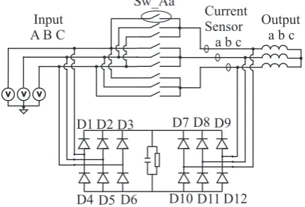
V V V
D1 D2 D3
D4 D5 D6
D7 D8 D9
D10 D11 D12 Input
A B C
Output a b c Current
[image:1.595.320.537.253.400.2]Sensor a b c Sw_Aa
Fig. 1: Circuit Diagram of the Matrix Converter with the Clamp Circuit
possible current recirculating paths when an open circuit fault occurs. However, neither simulation result nor experimental result is provided to validate the idea.
This paper presents the matrix converter current recirculat-ing behavior durrecirculat-ing an open circuit fault condition when a clamp circuit is implemented. The proposed idea is validated using SYNOPSYS SABER simulation tool.
II. MATRIXCONVERTEROPERATIONDURINGANOPEN CIRCUITSWITCHFAULT
Matrix converters provided no free-wheeling mechanism, so a clamp circuit is needed to protect it from over-voltage during open-circuit fault conditions as shown in Fig 1. Normally, the matrix converter input terminals should not be short circuited because it is fed by a voltage source. On the other hand, an output phase of a matrix converter must never be open circuited due to inductive load nature [1]. Hence, the switching duty cycle of the matrix converter must satisfy the condition expressed in equation 1.
0≤mhk ≤1, h=A, B, C, k=a, b, c. mAa+mBa+mCa= 1 mAb+mBb+mCb= 1
mAc+mBc+mCc= 1
TABLE I: Valid SVM switching configurations for matrix converters [6]
Switching Switches configuration On
+1 SAaSBbSBc
−1 SBaSAbSAc
+2 SBaSCb SCc
−2 SCaSBbSBc
+3 SCaSAbSAc
−3 SAaSCb SCc
+4 SBaSAb SBc
−4 SAaSBbSAc
+5 SCaSBbSCc
−5 SBaSCb SBc
+6 SAa SCb SAc
−6 SCaSAb SCc
+7 SBaSBbSAc
−7 SAaSAbSBc
+8 SCaSCb SBc
−8 SBaSBbSCc
+9 SAa SAbSCc
−9 SCaSCb SAc
0A SAa SAb SAc
0B SBaSBbSBc
0C SCaSCb SCc
Variables mhk are the duty cycles of nine bidirectional
switches Swhk in the matrix converter. The variable h
rep-resents the input side andkrepresents the output side. Space Vector Modulation (SV M) method is used in this paper.The
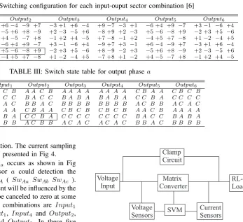
18active vectors and3 zero vectors are presented in TABLE I. In SV M, the choice of which active vectors to apply is dependent on the input-output sector combinations as shown in TABLE II [6].
In order to demonstrate clearly how the outputs connect to the inputs during any input-ouput sector combination, TABLE III is presented to show which input phase is connected to the output phase aat any sector combination.
Output current sensors required for control purposes are usually placed after the clamp circuit. However, in this paper, the current sensors are connected in-between the switch matrix and the RL-load, ahead of the clamp circuit connection in order to implement fault detection technique [14]. When a switch open-circuit fault occurs, the current recirculating path can be classified into two types. For a type 1 open-circuit as shown in Fig 2, load currents recirculate only through the output side of the clamp circuit and back to the load side. In type1, output current sensors could not detect any current flowing through the matrix converter. During a type 2 open-circuit as shown in Fig 3, load currents recirculate through the input and output side of the clamp circuit, the matrix converter and back to the load side. For a type 2 recirculating path, output current sensors could detect the current flowing through the matrix converter. Taking sector combination ofInput5and Output2 for instance, Type1and type2current recirculating
paths are shown in Figure 2 and Figure 3. These two current recirculating paths are drawn during zero and active vector period respectively, since the output matrix converter current will be measured within the zero vectors [14] or within the active vectors for fault detection purpose.
Recirculating currents in the matrix converter, load and
V V V
D1 D2 D3
D4 D5 D6
D7 D8 D9
D10 D11 D12
Input
A B C
Output
a b c
Current
Sensor
a b c
Sw_Aa O-C fault
a
b
c
A B C
i (n)
outi (n)
load [image:2.595.106.227.110.321.2]i
clamp(n)
Fig. 2: Type 1 open-circuit current recirculating path
V V
V
D1 D2 D3
D4 D5 D6
D7 D8 D9
D10 D11 D12
Input
A B C
Output
a b c
Current
Sensor
a b c
Sw_Aa O-C fault
a
b
c
A B C
i (n)
outi (n)
load [image:2.595.307.547.318.484.2]i
clamp(n)
Fig. 3: Type 2 open-circuit current recirculating path
clamp circuit satisfy the Kirchhoff Current Law (KCL) as shown in equation 2. Where iload(n), iout(n) andiclamp(n)
are three phase load currents, matrix converter output currents, and clamp circuit output side currents respectively as shown in Fig 2 and 3.
3 X
n=1
iload(n) =
3 X
n=1
(iout(n) +iclamp(n)) = 0
3 X
n=1
iout(n) =− 3 X
n=1
iclamp(n)
(2)
TABLE II: Switching configuration for each input-ouput sector combination [6]
Output1 Output2 Output3 Output4 Output5 Output6
Input1 −9 +7 +3 −1 +6−4 −9 +7 −3 +1 +6 −4 +9−7 −3 +1 −6 +4 +9 −7 +3−1 −6 +4
Input2 +8−9 −2 +3 −5 +6 +8 −9 +2−3 −5 +6 −8 +9 +2 −3 +5−6 −8 +9 −2 +3 +5 −6
Input3 −7 +8 +1 −2 +4−5 −7 +8 −1 +2 +4 −5 +7−8 −1 +2 −4 +5 +7 −8 +1−2 −4 +5
Input4 +9−7 −3 +1 −6 +4 +9 −7 +3−1 −6 +4 −9 +7 +3 −1 +6−4 −9 +7 −3 +1 +6 −4
Input5 −8 +9 +2 −3 +5−6 −8 +9 −2 +3 +5 −6 +8−9 −2 +3 −5 +6 +8 −9 +2−3 −5 +6
[image:3.595.183.531.77.394.2]Input6 +7−8 −1 +2 −4 +5 +7 −8 +1−2 −4 +5 −7 +8 +1 −2 +4−5 −7 +8 −1 +2 +4 −5
TABLE III: Switch state table for output phasea
P hasea Output1 Output2 Output3 Output4 Output5 Output6
Input1 C B C B A A C B A A A A A A A A C B A A C B C B
Input2 C C C C B A C C B A B A B A B A C C B A C C C C
Input3 A C A C B B A C B B B B B B B B A C B B A C A C
Input4 A A A A C B A A C B C B C B C B A A C B A A A A
Input5 B A B A C C B A C C C C C C C C B A C C B A B A
Input6 B B B B A C B B A C A C A C A C B B A C B B B B
applied to the space vector modulation. The current sampling point for fault detection purpose is presented in Fig 4.
When bidirectional switch SwAa occurs as shown in Fig 2 and Fig 3, output current sensor a could detection the zero current during zero vector 0A ( SwAa SwAb SwAc ).
However, output phasebandccurrent will be influenced by the output phaseacurrent, and could be canceled to zero at some sector combinations. These sector combinations are Input1
and Output5, Input4 and Output1, Input4 and Output2, Input5 and Output1, Input5 and Output2. In these five
sector combinations, type 1 recirculating path presented in Fig 2 will occur during the output currents sampling period.
Taking sector combination Input5 and Output2 for
in-stance, output phaseb andc are connected to the input phase
A in zero vector0A. Since clamp circuit diode D7 conducts
(Iouta≤0), the current recirculating path conducts through
the diode connecting to the most negative voltage. In addition, considering the current direction of Ioutb and Ioutc, the
output phase voltages V outb and V outc are more negative thanV inAdue to the voltage drop of the bidirectional switch during the zero vector 0A period. Therefore, only the output
side of the clamp circuit will recirculate during zero vector
0A as shown in Figure 2. Since no current will recirculate to
the input side clamp circuit and back to the output current sensors, current sensorsb andcwill detect zero current and a false diagnosis will occur. This false diagnosis indicates that
SwAb and SwAc are open-circuit faults. However, They are both healthy.
In order to avoid a false diagnosis mentioned above, more expert knowledge is required such as input voltage amplitude and direction, output current amplitude and direction, and nine bidirectional switching states information to contribute to a fault detection technique.
III. SIMULATIONDETAILS
A simulation of a matrix converter with close loop current operation system has been created using SYNOPSYS SABER. The block diagram of the matrix converter system is presented in Fig 5. The converter is switched with the SVM method and
Current Sensors
RL-Load Matrix
Converter Clamp Circuit
Voltage Input
Voltage
[image:3.595.317.540.286.390.2]Sensors SVM
Fig. 5: Block diagram of the matrix converter simulation model
the output current is regulated by a PI compensated control loop.
A. Parameters of the simulation
Three phase input voltages and frequency are set to be
60V and 50Hz respectively. The reference balanced three phase output currents are set to be 10A rms, with the output frequency set to 180Hz. In addition, the SVM switching sequence is 0C−> V1− > V3− >0A− > V4−> V2−>
0B− >0B−> V2− > V4−> 0A−> V3− > V1−>0C
as shown in Fig 4. Where V1, V2, V3, V4 are the four active
vectors as presented in Table II.
IV. RESULTS ANDANALYSIS
Simulation results are obtained for all36input-output sector combinations when an open circuit bidirectional switchSwAa
fault condition occurs. Specifically, current sensorbandcwill detect the zero current within zero vector0Aperiod among all
the possible 5 sector combinations of Input1 andOutput5, Input4 and Output1, Input4 and Output2, Input5 and Output1, Input5 and Output2. Simulation results of sector
combinationInput5andOutput2are presented thoroughly in
Fig 6 to 8. Normal and open circuit operation output current waveforms are shown in Fig 6 (a) and (b) respectively.
0
CV
1V
30
AV
4V
20
BTs/2
Ts/2
I
sampleI
sampleI
sampleI
sampleI
sampleI
sample [image:4.595.102.496.85.154.2]0
BV
2V
40
AV
3V
10
CFig. 4: Current sampling points for fault detection purpose
0 0.005 0.01 0.015 0.02 0.025 0.03 −20
−10 0 10 20
time (s)
Current (A)
Iouta Ioutb Ioutc
(a) Normal operation
0 0.005 0.01 0.015 0.02 0.025 0.03 −20
−10 0 10 20
time (ms)
Current (A)
Iouta Ioutb Ioutc
[image:4.595.332.534.356.445.2](b) Open circuit fault operation
Fig. 6: Matrix converter output current under normal and open circuit fault operation
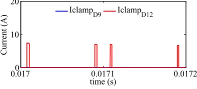
be seen that clamp circuit diodes D4, D7, D11, D12 are conducting. Both type 1 path shown in Fig 2 and type 2 path shown in Fig 3 occur in the simulation.
When magnifying the clamp circuit diodes current wave-forms presented in Fig 8, it can be seen that clamp circuit diodeD4 is not conducting within the zero vector0A period
under an open circuit fault condition. Therefore, only type 1 current recirculating path, as shown in Fig 2, is occurring and output phase b andc currents are canceled to zero as shown in Fig 8e.
0.0170 0.0171 0.0172 10
20
time (s)
Current (A)
IclampD1 IclampD4
(a) Clamp circuit diodeD1andD4current under open circuit
0.0170 0.0171 0.0172 10
20
time (s)
Current (A)
IclampD7 IclampD10
(b) Clamp circuit diodeD7andD10current under open circuit
0.0170 0.0171 0.0172 5
10 15
time (s)
Current (A)
IclampD8 IclampD11
(c) Clamp circuit diodeD8andD11current under open circuit
0.0170 0.0171 0.0172 10
20
time (s)
Current (A)
IclampD9 IclampD12
[image:4.595.332.530.618.707.2](d) Clamp circuit diodeD9andD12current under open circuit
17.0070 17.008 17.009 17.01 17.011 10
20
time (ms)
Current (A)
IclampD1 IclampD4
(a) Clamp circuit diodeD1andD4current under open circuit
17.0070 17.008 17.009 17.01 17.011 10
20
time (ms)
Current (A)
IclampD7 IclampD10
(b) Clamp circuit diodeD7andD10current under open circuit
17.0070 17.008 17.009 17.01 17.011 5
10 15
time (ms)
Current (A)
IclampD8 IclampD11
(c) Clamp circuit diodeD8andD11current under open circuit
17.0070 17.008 17.009 17.01 17.011 10
20
time (ms)
Current (A)
IclampD9 IclampD12
(d) Clamp circuit diodeD9andD12current under open circuit
17.008 17.009 17.01 17.011 −20
0 20
time (ms)
Current (A)
Iouta Ioutb Ioutc
[image:5.595.68.267.107.198.2](e) Magnified matrix converter output currents
Fig. 8: Magnified open circuit clamp circuit diode currents and output currents within zero vector0A period
V. CONCLUSION
This paper has presented a complete recirculating path analysis for matrix converters under an open circuit fault condition. When the current recirculating through the output-side clamp circuit and back to the load, there will be no current measured in the output current sensor, which could cause healthy output phases to be falsely diagnosed as open circuit. If the current recirculates through the matrix converter and back to the load, the output current can be detected in the output current sensor, which could avoid false diagnosis. This current recirculating rule is extremely valuable and can contribute to a fault detection and diagnosis system to improve the precision of the fault detection and diagnosis method in matrix converters.
REFERENCES
[1] P. W. Wheeler, J. Rodriguez, J. C. Clare, L. Empringham, and A. Wein-stein, “Matrix converters: a technology review,”Industrial Electronics, IEEE Transactions on, vol. 49, no. 2, pp. 276–288, 2002.
[2] B. Metidji, N. Taib, L. Baghli, T. Rekioua, and S. Bacha, “Novel single current sensor topology for venturini controlled direct matrix converters,”Power Electronics, IEEE Transactions on, vol. 28, no. 7, pp. 3509–3516, 2013.
[3] S. Ishikawa and T. Takeshita, “Input power factor control of three-phase to three-three-phase matrix converters,”IEEJ Transactions on Industry Applications, vol. 129, pp. 258–266, 2009.
[4] M. Venturini and A. Alesina, “The generalised transformer: a new bidirectional, sinusoidal waveform frequency converter with continu-ously adjustable input power factor,” inPower Electronics Specialists Conference, 1980. PESC. IEEE. IEEE, 1980, pp. 242–252.
[5] P. W. Wheeler, J. C. Clare, L. Empringharn, M. Bland, and M. Apap, “Gate drive level intelligence and current sensing for matrix converter current commutation,” Industrial Electronics, IEEE Transactions on, vol. 49, no. 2, pp. 382–389, 2002.
[6] D. Casadei, G. Serra, A. Tani, and L. Zarri, “Matrix converter modu-lation strategies: a new general approach based on space-vector repre-sentation of the switch state,”Industrial Electronics, IEEE Transactions on, vol. 49, no. 2, pp. 370–381, 2002.
[7] P. Wheeler, J. Clare, L. De Lillo, K. Bradley, M. Aten, C. Whitley, and G. Towers, “A comparison of the reliability of a matrix converter and a controlled rectifier-inverter,” inPower Electronics and Applications, 2005 European Conference on. IEEE, 2005, pp. 7–pp.
[8] M. Aten, G. Towers, C. Whitley, P. Wheeler, J. Clare, and K. Bradley, “Reliability comparison of matrix and other converter topologies,”
Aerospace and Electronic Systems, IEEE Transactions on, vol. 42, no. 3, pp. 867–875, 2006.
[9] L. Empringham, L. De Lillo, S. Khwan-On, C. Brunson, P. Wheeler, and J. Clare, “Enabling technologies for matrix converters in aerospace applications,” inCompatibility and Power Electronics (CPE), 2011 7th International Conference-Workshop. IEEE, 2011, pp. 451–456. [10] R. Peuget, S. Courtine, and J.-P. Rognon, “Fault detection and isolation
on a pwm inverter by knowledge-based model,” inIndustry Applications Conference, 1997. Thirty-Second IAS Annual Meeting, IAS’97., Confer-ence Record of the 1997 IEEE, vol. 2. IEEE, 1997, pp. 1471–1478. [11] R. L. de Araujo Ribeiro, C. B. Jacobina, E. R. C. Da Silva, and A. M. N.
Lima, “Fault-tolerant voltage-fed pwm inverter ac motor drive systems,”
Industrial Electronics, IEEE Transactions on, vol. 51, no. 2, pp. 439– 446, 2004.
[12] C. Brunson, L. De Lillo, L. Empringham, P. Wheeler, and J. Clare, “Matrix converter clamp current reconstruction for fault detection,” in Power Electronics, Machines and Drives (PEMD 2012), 6th IET International Conference on. IET, 2012, pp. 1–6.