A Low Capacitance Single-Phase AC-DC Converter
with Inherent Power Ripple Decoupling
Davide Gottardo, Liliana De Lillo, Lee Empringham, Alessandro Costabeber
PEMC Research GroupDepartment of Electrical and Electronic Engineering University of Nottingham
Email: eexdg6@exmail.nottingham.ac.uk
Abstract—This paper proposes a new single-phase AC-DC conversion topology with inherent power ripple decoupling, based on the combination of a PWM H-bridge inverter, an AC side LC filter and a ZVS line commutated H-bridge. A capacitor on the AC side is used as power decoupling element. By appropriate selection of the capacitor voltage, the power ripple at twice the AC frequency can be cancelled from the DC side instantaneous power, achieving negligible DC voltage ripple using a smaller total capacitance compared to traditional solutions.
Recently, several solutions using the concept of Ripple-Port have been proposed that reduce the overall capacitance. However, they usually need at least a dedicated PWM half-bridge leg, adding switching loss, and a separate LC tank. Instead, the proposed topology integrates the ripple compensation in the AC/DC conversion stage, exploiting the AC filter and minimising additional loss thanks to the ZVS of the additional H-bridge.
The concept of the steady state operation of the proposed converter is described analytically and validated in simulation using MATLAB Simulink and PLECS.
This work is being developed at University of Nottingham within the framework of project SENSIBLE.
I. INTRODUCTION
The diffusion of distributed generation and energy storage solutions is resulting in a growing need for single-phase AC-DC converters capable of unidirectional or bidirectional power flow, with rated powers often exceeding 1kW. Consequentially, a growing interest is arising in trying to develop more com-pact, efficient, reliable and inexpensive power converters that match those specifications. These converters can be generally intended for grid-connected or standalone applications.
One of the biggest problems of traditional single-phase power converters is the DC-link voltage ripple, caused by the oscillating nature at twice the AC frequency of single-phase instantaneous power. The power ripple requires the presence in the converter of a energy storage device in order to obtain power decoupling, i.e. to provide the power ripple at twice the AC frequency with negligible impact on the DC voltage.
The simplest and most common solution for this problem is to use a DC-link capacitor. This involves very high ca-pacitance to contain voltage ripple, thus limiting the choice to electrolytic capacitors, that degrade reliability [1]. A large capacitor is needed because most of the energy stored in the DC-link capacitor does not contribute to power decoupling.
Many different approaches have been made in order to overcome this problem [2][3][4][5][6]. A comprehensive
re-view of those solutions is found in [7]. All those solutions make use of additional switches in order to control the power flowing in one or more power decoupling elements, usually grouped in a Ripple-Port, a dedicated section of the converter which is only used to provide the ripple power component. The presence of additional components for the Ripple-Port is essential in order to reduce the overall capacitance but it also involves higher costs, losses and reliability issues related to higher part count. In fact, operating a converter at unity power factor and injecting an active power P, the average of the absolute value of the power processed by the port is
2
πP. This is processed by the power decoupling elements, and the following equation introduced in [4] can be used as an approximated evaluation of the impact of the Ripple-Port on the total conversion efficiency:
η=ηmain− 2
π(1−ηbuf f er) (1)
whereηmainis the efficiency of the main inverter/rectifier and ηbuf f eris the efficiency of the additional section that provides power decoupling.
In [5] Caceres and Barbi proposed a power converter ca-pable of power decoupling without using additional switches. A slightly different topology that exploits the same power-decoupling concept was introduced by Vasquez et.al. in [6]. The basic idea is that ripple power decoupling can be achieved integrating the Ripple-Port in the converter exploiting the LC output filter, rather than providing it with a dedicated circuit. This will minimise the need for additional components and their impact on efficiency and cost, while reducing the total capacitance. However, the capacitance needed tends to be higher than Ripple-Port based solutions.
This paper proposes a new topology built on the original concept proposed in [6] but completing it with a ZVS line-commutate H-bridge on the AC side, that can further reduce the converter capacitance with a limited increase in the com-plexity. The outcome is that values of total capacitance that are competitive with Ripple-Port solutions can be achieved with an integrated approach were no additional PWM legs are needed and the impact on the efficiency of the converter can be minimised.
V1 C1
L1 L2
I1
I2 V2
C2 Vdc
[image:2.612.61.289.51.122.2]Lg Vg
Fig. 1. Dual DC-DC [6]
procedure for the AC side capacitor used for power decou-pling. The design has been validated in a closed loop time domain simulation and compared with Ripple-Port solutions, showing promising performances.
II. POWER DECOUPLING
The energy balance of a converter can be expressed as in eq.2, where E(t) it the function of energy stored in the converter over time, t0 is an arbitrary instant of time, and
Pin,Pout are the power flowing in and out of the converter.
E(t)−E(t0) =
Z t
t0
Pin(t∗)−Pout(t∗)dt∗ (2)
Assuming the power transferred from the DC source to the grid to be constant and equal toP, i.e. ideal power decoupling is in place, the inverter to operate at unitary power factor and neglecting losses, the difference between the instantaneous powers flowing in and out the inverter is calculated as follows:
Vg(t) = √
2Vgsin(ωt) Ig(t) = √
2P Vg
sin(ωt) (3)
Pout=Vg(t)Ig(t) =P[1−cos(2ωt)] Pin=P (4)
Pin(t)−Pout(t) =Pcos(2ωt) (5)
Where Vg is the RMS line voltage andω is line pulsation. Substituting in 2, the result is:
E(t)−E(t0) =
Z t
t0
Pcos(2ωt∗)dt∗ (6)
Energy stored in the reactive elements is a function of the voltages in capacitors and current in inductors. For simplicity, the converter is assumed to be designed such that the energy stored in inductors and in small size filter capacitors is negligible, so that only few power ripple decoupling capacitors are taken into account in the power balance.
E(t) =1 2
X
i
CiVi2(t) (7)
Substituting 7 in 6 results is a relation between voltages in power decoupling capacitors over time, valid for all the topologies with capacitive decoupling.
1 2
X
i Ci
Vi2(t)−Vi2(t0)
=
Z t
t0
Pcos(2ωt∗)dt∗ (8)
time [s]
0 0.005 0.01 0.015 0.02
Voltage [V]
-500 0 500
Vg(t)
V1(t)
V2(t)
time [s]
0 0.005 0.01 0.015 0.02
Current [A]
-10 -5 0 5 10
Ig(t)
I1(t)
[image:2.612.317.548.63.327.2]Ic(t)
Fig. 2. Voltage and current waveforms VDC = 500V, P = 1kW,C1=C2= 28µF
III. INHERENT RIPPLE POWER DECOUPLING CONCEPT
In [5] Caceres and Barbi proposed a new type of DC-AC converter, composed of two independent DC-DC Boost converters. Vasquezet. al.extended the same concept to Buck and Buck-boost converters[6], as shown in figure 1 for the Buck topology. Despite their simple structure, those DC-AC converters based on the dual connection of DC-DC converters provide significant advantages:
• Power ripple decoupling exploiting the AC capacitors, achieved controlling the common mode voltage generated by the two converters, without a bulky DC-link capacitor and without additional switches;
• The same capacitors used as energy storage for power decoupling also work as filters.
Being the two arms of the converter identical, they are modulated so that each of them produces an output voltage referred to the negative of the DC link which is a line frequency sinusoid at the grid frequency with half the desired grid voltage amplitude, added to a common mode voltage used to control the instantaneous power flowing in C1 and
C2. The two sinusoidal components at the grid frequency are
in phase opposition, so that the difference between the two output voltages is equal to the desired voltage on the grid side.
in the next subsection, and will be extended later with the introduction of the new proposed topology.
1) Analysis of the capacitors voltages under ideal power ripple compensation: In order to calculate the desired steady-state value of voltages in capacitors V1 and V2, equation 8
can be used. Since the unknown functions are two another constraint is needed, which is that the differential voltage must be equal to line voltage.
V1(t)−V2(t) =Vg(t) = √
2Vgsin(ωt) (9)
The voltages at time t = t0 must be known too. Choosing
t0 = 0 simplifies the problem, since at t = 0 grid voltage
is zero (according to 3) and so V1(0) =V2(0). The resulting
voltages are:
V1(t) =
r P
2ωCsin (2ωt)− V2
g
2 sin(ωt)
2
+V2 0 +
Vgsin(ωt) √
2 (10)
V2(t) =
r P
2ωCsin (2ωt)− V2
g
2 sin(ωt)
2
+V2 0 −
Vgsin(ωt) √
2 (11) Where C1=C2=C andV1(0) =V2(0) =V0.
Since all ripple power is compensated byC1andC2, ideally
no voltage ripple is present on the DC link, with exception for PWM frequency ripple. Since the waveforms of voltages V1
andV2are a function ofV0andCfor a given power level and
a given grid voltage, particular attention must be paid in the choice ofCandV0in order to provide power decoupling while
respecting the constraints of minimum and maximum voltage that can be generated by the PWM bridge. In particular, V0
is an important degree of freedom, because it can be selected to respect the constants, at the same time trying to use the minimum value for the decoupling capacitors C.
2) Analysis of the converter currents under ideal power ripple compensation: The currents flowing in each capacitor IC1(t) and IC1(t) are calculated knowing their voltage over
time, and the currents flowing in each arm of the bridgeI1(t)
andI2(t)as sum of the capacitor current and grid current.
IC1(t) =C
d
dtV1(t) IC2(t) =C d
dtV2(t) (12)
I1(t) =IC1(t) +Ig(t) I2(t) =−IC2(t) +Ig(t) (13) In figure 2 the waveforms of voltage and current are shown for a specific choice of the operating point, C andV0. Since
the current I1 and I2 are equal and opposite in sign, only I1 is reported. In the intervals around line current peaks theIC1
current has opposite sign with respect to the grid current during positive half-wave, and has the same sign during the negative half-wave. Since the current I1 flowing through the bridge is equal to the sum of the two, the peak current through the bridge is higher than the grid current peak, having a negative impact on the resulting RMS value. For example, using the same parameters as in figure 2, the RMS value of grid current is 4.35 A,I1,RM S andI2,RM S are 4.68 A and the RMS current
V1 C L1
Lg I1
I2 V2
Vdc Vg
Ig
[image:3.612.314.557.48.377.2]V1’
Fig. 3. Proposed topology
time [s]
0 0.005 0.01 0.015 0.02
Voltage [V]
0 200 400 600
Vg(t)
V1(t)
V2(t)
time [s]
0 0.005 0.01 0.015 0.02
Current [A]
-5 0 5 10
I1(t)
I2(t)
[image:3.612.52.300.232.315.2]Ic(t)
Fig. 4. Voltage and current waveforms VDC= 500V, P = 1kW, C= 38µF
in the capacitors are 1.74 A. Moreover, the two capacitors do not completely cooperate in providing power decoupling, since often one is charging while the other is discharging. This provides the intuition about the fact that power decoupling can be optimised by introducing suitable modifications in the topology. This leads to the new proposed topology, that uses the inherent power decoupling concepts but further reduces the capacitor needed for power decoupling.
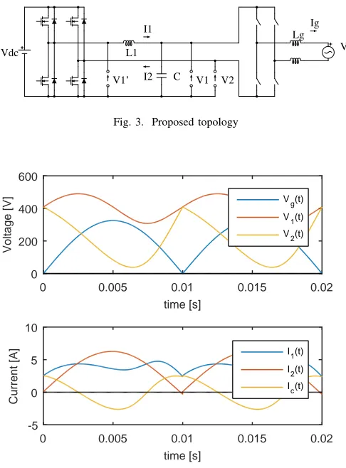
IV. PROPOSED TOPOLOGY
This proposed topology is obtained by adding to the previ-ously analysed topology a soft-switched line-commutated H-bridge switched at the zero crossings of the line voltage (ZVS) and removing one of the two capacitors, as shown in figure 3. This topology is able to provide power decoupling as the previously discussed one, while having significant advantages:
• Lower total capacitance needed;
• High efficiency of the PWM H-bridge;
1 L1 s
-1
|u|
I1 V1’
V2
Cs 1
1 Lg s
V1
Ig
[image:4.612.64.284.52.192.2]Vg RB
Fig. 5. Control model
Since only one capacitor is used, its voltage waveform VC(t)can be derived directly from eq.8:
VC(t) =
r P
ωCsin 2ωt+V
2
0 (14)
IC(t) =
Pcos 2ωt q
P
ωCsin 2ωt+V 2 0
(15)
V1(t) =VC(t) V2(t) =VC(t)− |Vg(t)| (16)
I1(t) =|Ig(t)|+IC(t) I2(t) =|Ig(t)| (17)
The first harmonic component of the capacitor current is similar in magnitude to the first harmonic of rectified grid current, and almost opposite in phase. Since the high-frequency bridge arm current I1 is the sum of the two, the
result is that the current waveform has an high DC component and low AC ripple, leading to lower RMS and thus better efficiency of the converter, compared to the original topology. For example, using the same parameters as in figure 4, the RMS value of grid current and I2,RM S is 4.35 A, I1,RM S is 3.95 A and the RMS current in the capacitor is 1.86 A. This should widely compensate the conduction losses in the line-commutated bridge. While voltage ripple in capacitors is bigger in [6], the total capacitance needed in the new topology is significantly lower.
Another advantage of this novel topology is that, as visible from the main current and voltage waveforms in fig.4, the current flowing in the PWM bridge arms is unidirectional, if unidirectional power flow is required. This is helpful because, in case of an application with unidirectional power, a diode and a switch in the high-frequency bridge are not needed, saving costs.
Since the line-commutated bridge always operates in soft-switching, switching losses are removed. For this reason, in the case in rectifier mode (power flowing only from grid to DC load), the low-frequency additional bridge can be simply made of diodes, while if the opposite power flow is required also thyristors can be used. The obvious drawbacks of this topology are conduction losses in the additional bridge and higher part counts.
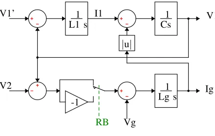
V. CONTROL CONCEPT
The proposed converter has to be able to control grid current and capacitor voltage. In order to do so, a possible control architecture is proposed. The model of the system is shown in figure 5. The control of the converter can be split, so that one PWM bridge leg can be used to control the capacitor voltageV1, thus taking care of power ripple decoupling, while
the other leg controls grid current according to the desiredP, independently. This is possible because the passive net formed by inductor L1, capacitor C1 and grid inductor Lg is by all
effects a LCL filter, that prevents the action of the first bridge leg to quickly affect grid current, thus effectively decoupling the control structure.
The line-commutated H-bridge does not directly interfere with current control, since it is operated at ZCS and ZVS, and the current flowing in inductor Lg is the non-rectified grid one, but the sign of voltagesV1 andV2 is inverted every
half-cycle. For this reason it is sufficient to change the sign of the output of the controller according to the position of the bridge. Since the steady-state waveform of the voltage V2 is known analytically (see previous section), its value is
added as afeed-forward to the output value of the controller. The implementation of the feed forwardof V2 is particularly
helpful for the provision of the high-frequency components of its waveform.
The control structure for V1 is very simple, since it isn’t
affected by the line-commutated bridge. The only perturbation here is the rectified grid current, that contributes to discharge the capacitor C1, but its high-frequency components are
fil-tered by the large capacitance.
VI. CAPACITOR ANDV0DESIGN
The value of V0 should be calculated to provide power
ripple decoupling with minimum total capacitance C. This is intuitively achieved when the voltage ripple applied to the capacitor is maximum, while respecting the constraints in terms of minimum and maximum voltage that can possibly be modulated by the PWM bridge.
The maximum ripple boundaries correspond to the voltage constraints that can be written as:
maxV1(t) =V1(t0) =Vmax minV2(t”) =V2(t”) =Vmin (18) It can be easily seen that in case ofV1the maximum value
corresponds tot0= 4πω, resulting in:
r P ωC +V
2
0 =Vmax (19)
Thus:
V0=
r V2
max−
P
C (20)
TABLE I
COMPARISONCACERES-VASQUEZ[6] / PROPOSED TOPOLOGY
[6] Proposed [6] Proposed
Vdc P Irms Irms Ctot Ctot
[V] [kW] [A] [A] [µF] [µF] 400 1 7.73 5.87 150 101 500 1 6.62 5.87 56 38 600 1 6.42 5.88 31 22 400 5 38.69 29.35 750 507 500 5 33.11 29.36 281 191 600 5 32.11 29.40 159 113 400 10 77.38 58.70 1500 1000 500 10 66.23 58.72 562 383 600 10 64.22 58.80 318 227
overcome this problem the minimization ofV2is approximated
as the minimization of its two components, leading to:
r
− P
ωC +V
2 0 −
√
2Vg=Vmin (21)
Solving the system of eq. 20 and 21 yields the approximated values of C and V0.
C=2P ω
1
V2
max−Vmin2 −2Vg2−2
3 2VgVmin
(22)
V0=
1
√
2
q V2
max+Vmin2 + 2Vg2+ 2
3
2VgVmin (23)
This approximated value of capacitance is higher than the minimum needed to respect the constraints, since the minimum value of voltage V2 calculated with this capacitance will be
higher than Vmin. This sub-optimum solution could be used when a rapid design procedure is desirable.
Instead, in order to get the correct optimum solution an iterative method can be used. Defining εk the difference between the calculated minimum ofV2k andVmin at the step k, the problem can be iterated as following:
(
maxVk
1(t0) =Vmax minVk
2(t”) =Vmin−Pki=1εi
(24)
The iteration can be stopped when sufficiently small values of εk are reached.
Capacitor sizing has to be done considering the worst case scenario of maximum power transfer, since it involves the highest voltage ripple in the capacitor itself. In that case, the value of V0 is fixed by eq. 20. In case of a required power
lower than the rated one,V0 can be regulated to some limits,
for example, to maximize the efficiency of the converter. A similar procedure, with some minor modifications that are omitted here, can be used for the sizing of parameters in [6].
TABLE II
COMPARISON WITH EXISTING TOPOLOGIES
P f Vg Vdc C
[kW] [Hz] [VRM S] [V] [µF]
Wang 15 233 150 540 150(200) 76 Krein 0.2 60 120 400 (3.3) 3.7
Qin 2 60 120 400 430 73
VII. COMPARISON
Several designs were computed for different values of DC link voltage and peak power, assigning Vmax=VDC−10V andVmin = 10V in order to leave a gap for control actions. The values of capacitance andV0were then used to derive the
values of RMS current in the two arms of the PWM bridge. The values of the column IRM S shown in table I are the root of sum of the squares of the calculated values of RMS current flowing through each bridge leg (pI2
1RM S+I22RM S), while the ones of the column Ctot are the total capacitance used. The results prove the benefits of the novel solution in terms of lower RMS current in the high-frequency bridge and minor total capacitance needed. The voltage of the grid is 230V RMS with a frequency of 50Hz.
If a certain DC link voltage is chosen, and assuming grid voltage independent from injected power, RMS currents and total capacitance grow linearly with power. In [6] a certain amount of power is circulating between the power decoupling capacitors. For this reason, since considerably higher values of capacitance are required if DC voltage is low, the total RMS current grows significantly, while in the proposed topology total RMS current is almost independent from DC voltage.
For these reasons, the proposed solution exhibits higher efficiency in the PWM bridge, at the cost of additional losses in the line-commutated one, that are anyway limited to conduction losses.
Further comparison have been made with well known power decoupling strategies, such as those described by Wang et.al.
[2], Kreinet.al.[3] and Qin et.al.[4]. The power injected in the grid and line voltage and frequency indicated in each paper were used for designing the proposed new topology, in order to compare the total capacitance.
The results are shown in table II. The first value of capac-itance indicated is the one reported in the papers, and the second is the one of the proposed topology. In [2], Wang
et.al used a 200µF capacitor in their prototype, however the theoretical minimum capacitance needed, which is the one significant for comparison, is reported to be 150µF. In [3] the used capacitance was not explicitly indicated, but since the capacitor was fully discharged every half cycle, its value can be calculated knowing the power as 3.3µF.
Current I1
t [s]
0.00 0.01 0.02
I1
[
A
]
0 2 4 6
(a)
Current I2
t [s]
0.00 0.01 0.02
I2
[
A
]
-10 0 10
(b)
Decoupling cap voltage
t [s]
0.00 0.01 0.02
V
1
[
V
]
300 400 500
(c)
Idc Current Spectrum
Frequency [Hz]
0 1000 2000
Id
c
[A
]
0 1 2
[image:6.612.54.298.48.693.2](d)
Fig. 6. Simulation results
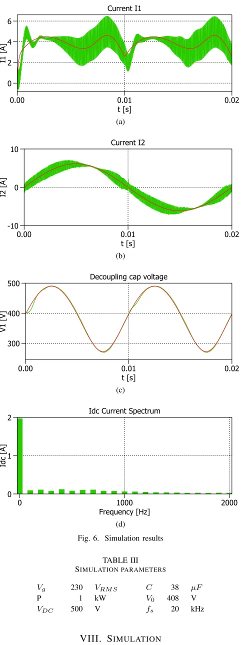
TABLE III SIMULATION PARAMETERS
Vg 230 VRM S
P 1 kW
VDC 500 V
C 38 µF
V0 408 V fs 20 kHz
VIII. SIMULATION
A time domain simulation of the proposed topology was implemented using Simulink and the PLECS toolbox.
Sim-ulation parameters are shown in table III. The same values were used to plot the waveforms shown in figure 2 and 4. The resulting waveforms of current and voltage in the PWM bridge arms and DC current spectrum are shown in figure 6. The DC source was modelled as an ideal voltage source with no series impedance. The DC current spectrum confirms the correct power ripple decoupling within the converter.
IX. CONCLUSION
This paper introduces a new AC-DC converter, suitable for low voltage distributed generation and/or energy storage systems, that provides inherent power decoupling without DC link capacitor and without a dedicated Ripple-Port. Active ripple energy storage is achieved using a line-commutated bridge operated at ZCS ZVS and a single decoupling capacitor connected on the AC side of the same PWM bridge that controls the grid current. A functional description is provided and the required total capacitance is derived analytically and compared to the capacitance of existing solutions based on concept of Ripple-Port. A simple design procedure to size the decoupling capacitor is proposed. A possible control scheme is proposed and validated in simulation. The results show that this topology offers a consistent reduction of the total capacitance needed for power ripple decoupling, making it a promising solution for developing cheap, reliable and efficient high power density single-phase converters, capable of unidirectional or bidirectional power flow.
ACKNOWLEDGMENT
This project has received funding from the European Unions Horizon 2020 research and innovation programme under grant agreement No 645963.
REFERENCES
[1] A. Lahyani, P. Venet, G. Grellet, and P. J. Viverge, “Failure prediction of electrolytic capacitors during operation of a switchmode power supply,”
IEEE Transactions on Power Electronics, vol. 13, no. 6, pp. 1199–1207, Nov 1998.
[2] R. Wang, F. Wang, D. Boroyevich, R. Burgos, R. Lai, P. Ning, and K. Rajashekara, “A high power density single-phase pwm rectifier with active ripple energy storage,”IEEE Transactions on Power Electronics, vol. 26, no. 5, pp. 1430–1443, May 2011.
[3] P. T. Krein, R. S. Balog, and M. Mirjafari, “Minimum energy and capacitance requirements for single-phase inverters and rectifiers using a ripple port,”IEEE Transactions on Power Electronics, vol. 27, no. 11, pp. 4690–4698, Nov 2012.
[4] S. Qin, Y. Lei, C. Barth, W. C. Liu, and R. C. N. Pilawa-Podgurski, “Architecture and control of a high energy density buffer for power pulsation decoupling in grid-interfaced applications,” in2015 IEEE 16th Workshop on Control and Modeling for Power Electronics (COMPEL), July 2015, pp. 1–8.
[5] R. O. Caceres and I. Barbi, “A boost dc-ac converter: analysis, design, and experimentation,”IEEE Transactions on Power Electronics, vol. 14, no. 1, pp. 134–141, Jan 1999.
[6] N. Vazquez, J. Almazan, J. Alvarez, C. Aguilar, and J. Arau, “Analysis and experimental study of the buck, boost and buck-boost inverters,” in
Power Electronics Specialists Conference, 1999. PESC 99. 30th Annual IEEE, vol. 2, 1999, pp. 801–806 vol.2.

![TABLE I [6] / P](https://thumb-us.123doks.com/thumbv2/123dok_us/8645530.372732/5.612.75.282.341.409/table-i-p.webp)