Charge sensing of single-hole tunneling
events using a single-electron transistor
Author:
Bram
van de
V
en
Graduation committee:
Prof. Dr. ir. W.G.
van der
W
iel
Dr. ir. F.A. Z
wanenburg
Msc. A. M
arquez
S
eco
Dr. E.S. K
ooij
Master Thesis
Nanotechnology
ii
c
A B S T R A C T
Charge sensing of single-hole tunneling events using a single-electron transistor (SET) is an important step towards the fabrication and read-out of hole qubits in silicon. The goal is the fabrication of an SET that is capacitively coupled to a single-hole tran-sistor (SHT). The metalic top gate and oxide materials used to fabricate these devices are varied to overcome several complication. It is demonstrated that using palladium gates, an accumulation SET and a depletion SHT can be formed. Titanium gates, with their enhanced stiction, are used to actively and passively sense hole tunneling events past the limit of direct transport at 4.2 K. However, due to the presence of an unintentional 2DHG, this could not be reproduced. Titanium-palladium devices are used to allow for the removal of the unintentional 2DHG using UV-ozone. Such a device is used to perform passive sensing past the limit of direct transport at 440 mK. Active sensing was not possible due to a high number of defects introduced during UV-ozone. Hafnium oxide is used in an attempt to remove the unintentional 2DHG by replacing the oxide interface. This interface is thought to contain negative charges that induce the 2DHG. Hafnium oxide is shown to reduces the 2DHG density as well as the turn-on voltage, making it a promising material for future devices.
A C K N O W L E D G E M E N T S
The work presented in this thesis would have never been possible without the help of many people to whom I would like to express my gratitude.
First of all I want to express my gratitude to my daily supervisor Alejandro Mar-quez Seco, who is always willing to help whenever possible, even when all the way in Spain. His positive teaching attitude always motivated me to give it my all. I wish to thank Wilfred van der Wiel and Floris Zwanenburg, for giving me the op-portunity to do this interesting research within the Nano-Electronics group. Floris’ feedback during the weekly meetings and his open door policy were very helpful, making it possible to get regular and relevant feedback on my progress. I would like to acknowledge Sergey Amitonov for his vast knowledge and great advice in the cleanroom. Thank you, all my fellow master students for the relaxing conversations and specifically Thijs van der Berg, for our discussions on the research, which helped me to reach the understanding I have now. And what is research without technicians. Thijs Bolthuis, Johnny Sanderink and Martin Siekman helped me with many practical aspects of the research. I want to thank everyone in the Nano-Electronics group who have made my time here unforgettable.
Of course moral support is one of the most important things when performing such a challenging task. Therefore, I want to thank my parents for participating in the regular conversation about the research. Thanks to my friends with whom I could always have fun and relax. Finally, I want to thank Maaike Rump, who supported me throughout the project.
C O N T E N T S
1 i n t r o d u c t i o n 1
2 t h e o r y 3
2.1 Quantum Dot . . . 3
2.2 Constant Interaction Model . . . 4
2.3 Quantum dot transport . . . 4
2.4 SET/SHT . . . 6
2.5 Charge sensing . . . 8
2.5.1 Sensitivity . . . 8
2.5.2 Passive Sensing . . . 9
2.5.3 Active Sensing . . . 9
2.6 Double Quantum Dot . . . 10
2.7 Charge traps and Annealing . . . 11
2.8 Two-dimensional hole gas . . . 12
3 f a b r i c at i o n 13 3.1 Wafer Fabrication . . . 13
3.2 Device Fabrication . . . 14
3.2.1 Electron beam lithography . . . 14
3.2.2 Cold Development . . . 15
3.2.3 Electron beam evaporation . . . 15
3.2.4 Atomic layer deposition . . . 16
3.3 The Design . . . 17
3.4 Devices . . . 17
3.4.1 Palladium . . . 18
3.4.2 Titanium . . . 19
3.4.3 Titanium-Palladium . . . 20
3.4.4 Hafnium Oxide . . . 21
4 m e a s u r e m e n t s e t-u p 23 4.1 Sample preparation . . . 23
4.2 Set-up . . . 23
4.3 Heliox . . . 24
5 r e s u lt s a n d d i s c u s s i o n 25 5.1 Palladium . . . 25
5.1.1 Electrons . . . 26
5.1.2 Holes . . . 26
5.2 Titanium . . . 31
5.3 Titanium-Palladium . . . 35
5.3.1 Dipstick measurements . . . 35
5.3.2 Heliox measurements . . . 39
5.4 Hafnium Oxide . . . 44
6 c o n c l u s i o n 49
viii Contents
7 o u t l o o k 51
1
I N T R O D U C T I O N
Quantum computers have been predicted to be able to solve specific problems in a more efficient way than classical computers. Using specific quantum algorithms it can become possible to, for example, perform simulations of complex optimization
problems and many particle systems [1]. Such a quantum computer uses quantum
bits (qubits) instead of bits. These qubits use the superposition of their quantum mechanical states to perform computation. This results in an exponential, instead of
linear, increase in computation speed with N bits [2]. One of the commonly
investi-gated systems, is the spin of an electron, a two-state quantum mechanical system. To be able to use electrons for this purpose, they need to be trapped, such that control, read-out and isolation from the environment are possible. This can be achieved using quantum dots which have discrete energy levels, on which single electrons can reside [3]. There are multiple ways to fabricate such quantum dots [4, 5,6]. This research focuses on gate-induced silicon quantum dots. Silicon is a semiconductor which can be purified to suppress nuclear spin, resulting in no perturbation associated with the
silicon lattice, which allows for high coherence times [7]. Furthermore, CMOS
tech-nology is widely used in modern computer fabrication, possibly allowing scaling of silicon qubits. The knowledge obtained during the thesis is beneficial for the fabrica-tion of silicon based qubits and indirect measurements of their state.
Two of the important challenges, when making a qubit, are read-out and control of the spin state of an electron. Directly reading out this spin state, results in loss of its information. Therefore, it is important to be able to indirectly measure this
state. One of the methods for doing this is spin-to-charge conversion [8,9]. Using a
charge sensor, it is possible to measure the tunneling events of a nearby charge. By inducing a difference in tunneling probability between two spin states, it is possible to measure the state of the electron indirectly. Which is known as spin-to-charge con-version. This difference can be achieved by splitting the two states using a magnetic
field, making use of Zeeman splitting [10]. The process of reading out the electron
spin using this method is known as single-shot readout [11, 12]. Similarly, it is pos-sible to measure the interaction of the spin states of two qubits, tunnel coupled to one another. Here the principle of Pauli spin blockade only allows spins with op-posite directions to tunnel. By sensing whether the charges move it is known if the qubits are in the same or the opposite state [13,14]. These kinds of spin to charge con-version techniques have been achieved using single-electron transistors (SET).[15,16].
For the second challenge, controlling the spin state of an electron, electron spin reso-nance (ESR) lines are often used. When running an alternating current through this line, an oscillating magnetic field is induced. Using this oscillating magnetic field on top of a constant magnetic field, spin-flips can be induced at the precession frequency
of the spin [17]. However, spin based qubits are not limited to electrons. It is also
2 i n t r o d u c t i o n
possible to control the spin states of holes. A hole is the counter part of an electron
which resides in the valence band instead of the conduction band [18]. Holes have
a higher spin-orbit coupling, which can make it possible to influence its spin state using electric instead of magnetic fields. Thus, it is possible to influence its spin
us-ing the same gate electrodes that are used to form the quantum dots [19]. Besides
a higher spin orbit coupling, holes also have a reduced hyperfine interaction. This results in longer coherence times due to a reduced interaction with the nuclear spins of nearby atoms [20].
To be able to perform spin state measurements on a single hole (or electron), the quantum dot may only contain one hole. It is often difficult to reach this single hole regime due to direct transport limitations. However, a charge sensor is able to sense tunneling events past the limit of direct transport, making the single hole regime more accessible.
In this project, the favourable qubit properties of holes are combined with the read-out possibilities of a SET charge sensor. Since both the hole and electron side require opposite electrostatic doping. When forming the quantum dots, this opposite doping
automatically is present a barrier in between them [21]. This barrier makes is
possi-ble to put the two devices close together without leakage, thus reaching a stronger capacitive coupling and a higher SET sensitivity [22].
2
T H E O R Y
In this chapter, the theory needed to understand the results presented in the thesis is described, starting with a basic description of quantum dots. The electronic transport through such a quantum dot, capacitively coupled to a source, a drain and a gate, is explained. The formation of gate defined quantum dots and how they are used for charge sensing is discussed.
2.1 q ua n t u m d o t
One of the most basic descriptions of a quantum dot (QD), is a nanometer sized metallic island that can be occupied by charge carriers like electrons of holes. Because the size of the island is comparable to the wavelength of the confined charge carriers
on the island, the QD has discrete energy levels [23]. Characterization of the energy
levels of such a QD can be done using electronic transport measurements by coupling the QD to a source, a drain and a gate so that current can flow through it. Such a system can be seen in figure 1: a gate strongly coupled to the QD, can be used to adjust the electrochemical potential of the QD by modifying the applied gate voltage
(Vg). However, before going into details about electronic transport through a QD it
is important to have a good understanding of its energy levels. These levels can be described using the constant interaction model [24].
Figure1: Schematic representation of a quantum dot that is connected to source and
drain contacts using tunnel barriers. This quantum dot is capacitively
cou-pled to a gate. Image taken from Kouwenhoven et. al. [5].
4 t h e o r y
2.2 c o n s ta n t i n t e r a c t i o n m o d e l
The constant interaction model is based on two assumptions. The first states that the Coulomb interaction between charges both inside and outside of the quantum
dot can be parameterised by the sum of all capacitances, C = CS+CD+∑CG. CS
and CD are the capacitive coupling to the source and drain, respectively, and ∑CG
is the coupling with all metal gates as well as other possible defects. The second assumption states that the energy level spacing of the QD does not depend on the
amount of electrons on the QD [9]. Using these assumptions, the total energy of a
QD containing N electrons is described by equation 1.
U(N) = [−|e|(N−N0) +CSVS+CDVD+CGVG]
2
2C +
N
∑
n=1
En(B) (1)
In this relation, −|e| is the electron charge and N0 is the amount of electrons in
the QD when no gate voltage is being applied [9][24]. The CSVS, CDVD and CGVG terms represent the voltage induced charges on the QD and can be continuously changed. The final term in equation (1) sums over the occupied single-electron levels
En(B). To describe transport through a QD, it is more convenient to work with
the electrochemical potential (µ). Equation 2 shows the electrochemical potential
required to add one electron to the QD [24].
µ(N) =U(N)−U(N−1)
= (N−N0−
1 2)Ec−
Ec
|e|(CSVS+CDVD+CGVG) +En (2) Using the gained understanding of the energy levels of a QD, electronic transport through this quantum dot will be explained.
2.3 q ua n t u m d o t t r a n s p o r t
To measure direct electronic transport through a QD, it needs to be tunnel-coupled to source and drain contacts, such that an electron can tunnel from the source to the QD and from the QD to the drain. This system is illustrated in figure 2. Electrons can only occupy the energy levels of the QD that are at or below the electrochemical potentials of the source, drain or both. These states are of equal or lower energy
mak-ing it energy-favourable for electrons to occupy them [5]. When an energy level is in
2.3 q ua n t u m d o t t r a n s p o r t 5
(A) (B)
Figure2: Schematic representations of the electrochemical potentials of a quantum
dot. (A) The electrochemical potential of the quantum dot is in between the electo-chemical potentials of the source and the drain. The system is in its single-electron transport regime. The number of electron on the quantum dot can alternate between N-1 and N. (B) The electrochemical potentials of the quantum dot do not fall in between the electrochemical potential of the source and drain. The system has a constant amount of electrons and is therefore in Coulomb blockade.
As mentioned, it is possible to manipulate the energy levels of the quantum dot by varying the gate voltage. By doing this, the energy levels can be swept between the source and drain, switching from single electron tunneling (figure 2(A)) to Coulomb blockade (figure 2(B)). When sweeping this gate voltage and measuring the current, peaks associated with the energy levels of the quantum dot can be observed (figure 3(A)) [24].
By varying the source-drain voltage, the separation between these peaks becomes smaller. When plotting differential conductance as a function of the source-drain voltage and gate voltage, Coulomb diamonds such as the one in figure 3(B), can be
measured [8]. In principle, there is a constant current inside the diamond-shaped
re-gions, the quantum dot is in Coulomb blockade, and the electron population on the QD is constant. At zero bias, two of the diamond corners are observed. At these gate voltages, the electrochemical potential of source, drain and QD are all in resonance, facilitating electron transport. The diamond edges indicate where the electrochem-ical potential of the source and quantum dot are equal. For edges with a positive slope, this indicates the gate voltages at which the final electron can still enter the dot from the source. The edges with negative slope indicates the lowest gate volt-age at which an electron, on this specific energy level, can leave the dot to the drain
[24,8]. The slopes of the diamond edges depend on the capacitive coupling between
the QD and source, drain and gate. This dependency is expressed byCG/(CG+CS)
6 t h e o r y
(A) (B)
Figure3: (A) Schematic plot showing the current through a quantum dot as a
func-tion of the gate voltage. This plot shows a Coulomb peak every time a single electron tunneling event takes place. Image taken from Hanson et.
al. [9]. (B) Biasspectroscopy, source-drain voltage versus gate voltage, in
differential conductance,dI/dVSD, showing Coulomb diamonds. The black
edges of the diamond show the onset of current. The grey lines indicate
transport through excited states. Image taken from Van Beveren et. al. [24].
2.4 s e t/s h t
Single-electron transistors are devices that use discrete energy levels to facilitate single-electron tunneling. These devices have been successfully fabricated in silicon
using Metal-Oxide-Semiconductor Field-Effect Transistors (MOSFET) [26]. In such
devices, a metal gate on top of the oxide is used to attract electrons (holes) to the semiconductor-oxide interface, in this case the Si-SiO2interface. By doing this, a
two-dimensional electron (hole) gas (2DEG, 2DHG) is formed. The formation of this gas
pushes the conduction band below (or valence band above) the Fermi energy (EF),
allowing electron (hole) transport to take place. By using two barrier gates to locally
deplete the 2DEG (2DHG), a quantum dot can be formed [27]. Figure 4(A) shows
the cross-section of such a device and figure 4(B) and (C) the corresponding energy diagram when the quantum dot is formed.
For such a device to function as a SET or SHT, there are three requirements that need
to be met. First, the energy between the discrete energy levels (charging energy, EC)
needs to be smaller than the thermal energy in the system, such that they do not overlap.
EC=
e2
C >KBT (3)
Wheree is the elementary charge of an electron, C the capacitive coupling of the dot
to its surroundings and KBT the thermal energy. Second, a charge carrier needs to
be located on the source, drain or island. In other words, the Heisenberg uncertainty principle needs to be overcome.
2.4 s e t/s h t 7
Where ∆E = Ec = e
2
C and the change in time equals the RC-time (∆t = RtC). Where
Rt is the tunneling resistance. Rewriting the equation results in.
e2
C ·R·C>h Rt >>
h e2
(5)
Finally, to be able to achieve Coulomb blockade, the source-drain bias needs to be smaller than the charging voltage.
Vbias <
e
C (6)
Oxide
Intrinsic Si
BL
BR
Lead gate
p++n++ n++ p++
2DEG/2DHG
QD
(A)
BL BR
(B)BL BR
(C)
Figure4: (A) Schematic cross section of the MOSFET device used to form a quantum
8 t h e o r y
2.5 c h a r g e s e n s i n g
Single-electron (hole) transistors are not only used for the formation of quantum dots. They are also used as very accurate charge sensors. This sensitivity comes from the gate voltage dependent Coulomb peaks. Since this gate can be made of any metallic material as long as it is capacitively coupled to the quantum dot. When, for example, there is another QD or charge defect in the vicinity of the QD and a charge is added or subtracted from this second QD, the sensor will feel the influence created by this extra charge. This results in the shift of the Coulomb peaks with respect to the gate voltage, as shown in figure 5(A). This shift causes a measurable change in current [22].
(A) (B)
Figure5: (A) A single Coulomb peak before and after the addition of a single-electron
to another quantum dot or charge trap near sensor QD has been sensed.
Figure taken from Zajac et. al. [22]. (B) Example of the result obtained
when using passive charge sensing. The vertical lines indicate the addition of charge to the sensed system. This can be a nearby quantum dot, charge defect or atom. Figure taken from Morello at. al. [12].
2.5.1 Sensitivity
It is important to understand how to increase the sensitivity of the sensor to be able to design reproducible charge sensing devices. It is shown in figure 5 that a
tunneling event of a single charge results in a Coulomb peak shift ∆V. However,
instead of looking at this change in voltage the corresponding change in current is measured. Hence, there are two ways to increase the sensitivity: either the change in voltage or the corresponding change in current can be increased. The change in voltage is dependent on the capacitive coupling between the two quantum dots and the surrounding metals. The relation is described in equation 7.
∆V= e·CSD
CS·CD
(7)
This relation shows that the sensitivity depends on two parameters: the ratio of
the capacitive coupling between the sensor and the dot (CSD), and the dot to its
surroundings(CD) (which includes all possible capacitances), and the charging energy
of the sensor (e/CS). The first is fairly self explanatory, when one charge is added
[image:16.595.77.475.239.372.2]2.5 c h a r g e s e n s i n g 9
is capacitively coupled. The ratio now gives the amount of charge changed in the sensor. Since the charging energy of the sensor is the energy needed to add one
electron or hole to the sensor, the shift (∆V) will be relative to this energy. The
second option is increasing the change in current for the same change in voltage. This happens when the slope of the Coulomb peak increases. The width of the peak
is dependent on the thermal energy KBT, the source-drain voltage and the tunnel
coupling to this source and drain. However, the source-drain voltages as well as the tunnel coupling influence the current or height of the coulomb peak. Therefore, one method of increasing the sensitivity is by measuring at lower temperatures. The source-drain voltage should be optimized to obtain a high current with a small width. The dependency of the sensitivity on the current through the sensor is the main reason why a single-electron transistor is more sensitive to charge changes than a single hole transistor. Due to the higher mobility of electrons, the current will be higher, resulting in a steeper slope and therefore a bigger change in current when a charge sensing event takes place. Charge sensing can be done in two ways: passively and actively, which will be discussed in the following subsections.
2.5.2 Passive Sensing
During passive sensing we look at the Coulomb oscillations (Coulomb peaks) of the sensor, without any type of feedback mechanism, while adding or removing charges from the to-be-sensed dot. Every time a charge is added or removed, these oscilla-tions will be shifted (figure 5(A)). This allows for a charge sensing method that is easy to execute. However, since the sensing event takes place at different positions along the coulomb peaks, the corresponding current change will now be dependent on this position and can become negligible. This is illustrated with the magenta line
in figure 6 [29]. A way to work around this problem is by measuring over multiple
coulomb peaks of the sensor. Such a measurement will result in an image similar to
figure 5(B) [12]. However, the coulomb peaks of the sensor are now visible, and the
desired output thereby more difficult to observer.
2.5.3 Active Sensing
10 t h e o r y
Figure6: The SET sensor current without compensation (magenta), is compared to
the QD its direct transport current (black). Fixed compensation is applied by linearly adjusting the sensor gate potential and the compensated (blue) then operates within a fixed range with a corresponding trans-conductance (orange), shows the increased signal using this compensation. Figure taken from Yang et. al. [29].
VSD[x+1] =VSD−βISD−∆VMDAC[x] (8)
AC[x+1] =AC[x] +
γ
∆VMD
ISD[x] (9)
Where the step size of the measured dot is described byVMD,ACis the ratio between
the capacitances of the QD to its lead gate and to the lead gate of the sensor. This ratio will be extracted from a gate-space measurement, by looking at how the peak
position changes for different voltages. ISD is the source-drain current at which the
sensor is operated and β the decay rate of the deviation of the current from its
de-sired value (I0). Finallyγis used to adjust the decay rate ofACback to its steady state
value. This feedback mechanism is used for some of the the measurements presented in chapter 5 [29].
2.6 d o u b l e q ua n t u m d o t
Instead of one, it is also possible to have two or more quantum dots in series or parallel. This could, for example, be achieved by adding an extra barrier gate, such that two islands, that are tunnel coupled to one another, are formed. The best way to analyze the amount of quantum dots in the system, is by measuring a charge stability diagram or gate space. This is done by sweeping two of the gates in the system. By doing this the device is swept through the Coulomb peaks of both the
quantum dots. Depending on the mutual capacitance (Cm) between the two dots,
the device will either be in the weak, intermediate or strong coupling regime. When
Cm ≈0 the quantum dots are weakly coupled. Therefore, their Coulomb peaks will
2.7 c h a r g e t r a p s a n d a n n e a l i n g 11
dot (figure 7(A)). When Cm ≈ 1 the dots are strongly coupled. The Coulomb peaks
of the quantum dots are equally coupled to both the gates and therefore will both be diagonal. Therefore the Coulomb peaks are at the same positions in gate space, see figure 7(C). Finally when the mutual capacitance is somewhere in between 0 and 1, the intermediary regime, both lines will be slightly slanted, as indicated in
fig-ure 7(B) [30]. In the devices we analyze in this thesis, this is the most commonly
observed variant. The second set of Coulomb peaks are the result of the formation of unintentional quantum dots caused by the presence of charge traps or Pb Centers.
(A) (B) (C)
Figure7: Schematic charge stability diagram of a double quantum dot system that is
coupled to at least two gates. (A) weak, (B) intermediate, and (C) strong inter-dot coupling are shown. The numbers inside of each cell indicate the number of electrons in each of the dots. Image taken from van der Wiel et. al. [30].
2.7 c h a r g e t r a p s a n d a n n e a l i n g
Silicon has four valence electrons, hence it requires four bonds to fully saturate its va-lence shell. In the bulk, each silicon atom binds to four other silicon atoms. However,
at the Si-SiO2, it is not always possible to form these four bonds. Which causes Pb
centers or charge traps to form (as shown in figure 8(A)) [31]. In this case, a charge
trap exists due to the unpaired valence electron of a dangling bond. This state can be occupied by individual electrons just like a quantum dot. When such a charge trap happens to be positioned underneath one of the barriers, these barriers will tunnel couple it to its surrounding. Due to its zero dimensional nature, an unintentional
quantum dot is formed underneath this barrier [32][33]. This extra quantum dot will
either be in series or parallel. When looking at the Coulomb peaks of the device, extra features will be present, resulting in a more chaotic behaviour. Fortunately, passiva-tion of these charge traps can be done by hydrogen annealing. At a high temperature,
300-400◦C, the device is exposed to a hydrogen environment. This hydrogen will, as
12 t h e o r y
(A) (B)
Figure8: (A) shows a Si/SiO2 interface before annealing. A P
b center exists at this
interface due to dangling bonds. (B) is a Si/SiO2 interface after annealing.
The Pb center is now passivated by a hydrogen atom. Images adapted from Etner [31].
2.8 t w o-d i m e n s i o na l h o l e g a s
In the devices used for the experiments shown in this thesis the oxide layer between
the silicon and metal gates is made from a SiO2-Al2O3 stack. It has been shown that
negative charges can be present at the interface between these layers [34]. In the used devices, systematically shown in figure 4(A), these negative charges lead to the
accu-mulation of positive charge at the Si-SiO2 interface resulting in a 2DHG that will be
present at all times (see figure 9). It has been previously shown that this hole gas can
be used to form depletion quantum dots [35]. However, the presence of the 2DHG
makes it difficult to form accumulation quantum dots.
SiO
2
Intrinsic Si
Al
2
O
3
p++
p++
2DHG
+ + + + + + + + + + + + + + + + +
- - - - - - - - - - - - - - - - - - - -
Fixed charge
Figure9: Illustration of the 2DHG (pluses) induced at theSi/SiO2interface by nega-tive charge (minuses) at the SiO2-Al2O3interface
The origin of the negative charge at the SiO2-Al2O3 interface is not yet fully
3
FA B R I C AT I O N
In this chapter, I describe the fabrication method of the self-made devices. The de-sign of the devices is explained with special focus on the important parameters. In this thesis four different types of devices are discussed. The devices, their names and differences are summarized in table 1. Finally, optical pictures and AFM scans of the fabricated devices are presented, including a discussion of their fabrication challenges.
Device name Metal top gate materials ALD oxide
Palladium Palladium Aluminum oxide
Titanium Titanium Aluminum oxide
Titanium-Palladium Titanium-Palladium Aluminum oxide
Hafnium Oxide Titanium Hafnium oxide
Table1: Table showing the different devices that were fabricated during the project.
3.1 wa f e r f a b r i c at i o n
To facilitate separate transport of holes and electrons, we fabricate two MOSFETs in close vicinity of one another. This is done using a near-intrinsic silicon wafer
(σ ≥ 10000 Ωcm) on which 200 nm of SiO2 is thermally grown. Photolithography
was used to define the areas in which boron and phosphorous are implanted to form separate p++ and n++ regions. To integrate the phosphorous and boron into the
silicon lattice, the system is rapidly annealed at 1000 ◦C. Using photolithography, a
8 nm thick high-quality silicon oxide layer is thermally grown at 900 ◦C to define
the region where the active MOSFET regimes are made. This process further helps the incorporation of the dopants into the lattice. Photolithography is once again used to define the regions where aluminum contact pads are sputtered on top of the boron and phosphorous-doped regions. For wafers used to fabricate specific devices,
as explained later, the SiO2 is covered with a 5 nm aluminum-oxide (Al2O3) layer
deposited using atomic layer deposition (ALD). This is an extra oxide layer reducing the amount of leakage through the oxide. It also functions as a sticking layer for specific metals that are deposited in a later stage of fabrication. On top of this layer, photolithography is used to fabricate Ti/Pt contact pads, the fabricated structure is shown in figure 10(A). Unfortunately, not all gate materials stick to these contact pads. Thus, for some of the devices, these pads are not fabricated during wafer fabrication (see figure 10(B)) but during the device fabrication. Finally, the wafer is diced into
1x1cm2chips that will be further processed to obtain the smaller structures required.
The wafer fabrication has been done by Sergey Amitonov and Alejandro Marquez Seco.
14 f a b r i c at i o n
(A) (B)
Figure10: (A) Optical microscope image of the basic device structure used for top
gate metals that stick to the Ti/Pt contact pads. (B) Optical microscope image of the structure used for top gate metals that do not stick to the Ti/Pt contact pads.
3.2 d e v i c e f a b r i c at i o n
The size and formation of the quantum dots are defined by the geometry of the metal top gates. We use electron beam lithography (EBL), electron beam evaporation and lift-off to make these barriers. The devices require two metal layers, each fabricated separately using the techniques mentioned. In between the two layers, atomic layer deposition is used to deposit the different oxides used. For the fabrication of the first gate layer, 55 nm of Poly methyl methacrylate (PMMA) is spin coated on top of the chip. For the second layer 80 nm of PMMA is used. The nanometer sized structures are patterned in this PMMA using electron beam lithography (EBL).
3.2.1 Electron beam lithography
EBL uses electrons to locally break the PMMA bonds. When putting the chip with exposed PMMA in a developer (IMBK:IPA, 1:3), the weakened bonds dissolve faster, revealing the desired pattern in the PMMA. When patterning the nanometer sized structures, the electrons are accelerated using an energy of 28 keV through a column
of 10 µm. 28 keV is the highest reliable acceleration energy in the used EBL system
3.2 d e v i c e f a b r i c at i o n 15
limitation, bigger structures, such as the contact pads, are patterned using lower acceleration energies. The proximity effect is less relevant for the big structures,
be-cause they don’t require much precision. Initially, 2 keV and 120 µm were used as
the acceleration energy and aperture, respectively. However, these settings resulted in badly defined PMMA edges (see figure 11(A)). Therefore, a switch to 10 keV and
60 µm was made. Using these setting we are able to fabricate well-defined edges
such as the ones shown in figure 11(B).
(A) (B)
Figure11: (A) AFM image of the edge of developed PMMA patterned using 2 keV
and (B) 10 keV.
3.2.2 Cold Development
Another technique used to reduce the structure size is cold development. The de-veloper (IMBK:IPA, 1:3), used to dissolve the exposed PMMA, is kept and used at
−15 ◦C instead of room-temperature. The developer has less energy to react with
the PMMA, resulting in a need for more broken bonds to be able to develop. This requires the use of a higher dose (number of electrons) during EBL patterning, to be able to develop (remove) the exposed PMMA. This high concentration will only be reached in the directly exposed parts, back-scattered electrons will have a much lower concentration compared to the targeted areas. Therefore, development in the prox-imity of the pattern is reduced when compared to room-temperature development [36].
3.2.3 Electron beam evaporation
16 f a b r i c at i o n
evaporation chamber and the position of the beam on the target. By combining this evaporation rate with the deposition time it is possible to very accurately grow nanometer thick layers. To only have metal structures in the EBL defined regions,
lift-off is used. We put the sample in dimethyl sulfoxide (DMSO) at 90 ◦C such that
the PMMA dissolves. The metal that has been deposited on top of the PMMA will let go since it has no attachment point to the substrate. This results in metal structures only on the exposed regions. Ultrasonication can be used to facilitate this process.
3.2.4 Atomic layer deposition
Atomic layer deposition (ALD) is a thin film deposition technique used to make highly conformal films. For the devices made, ALD is used to deposit the oxides
(except for the thermally grown SiO2). During ALD precursors, that react with the
surface of the sample, are cylced. The first cycle is used to deposit one of the desired materials, for example aluminum. A second cycle with the precursor for the oxygen
reacts with the deposited aluminum. These two cycles form one monolayer of Al2O3,
by switching between the two precursors the Al2O3 is grown layer by layer. Since
the reactions only take place at the surface, only a single layer of atoms is deposited for each precursor flush. This high quality oxide layer which is placed in between the barrier and top gate electrodes to prevent leakage. For this purpose, 5 nm thick oxides are used. The devices are also capped with 5 nm of the same oxide to protect the chip from the influence of outside interactions after fabrication. Finally, the same
machine is used charge traps are removed at the Si-SiO2 interface. This is dony using
hydrogen annealing at 400 ◦C and a pressure of 10 mbar. ALD and annealing have
3.3 t h e d e s i g n 17
3.3 t h e d e s i g n
The described processes are performed to fabricate a single-electron transistor capac-itively coupled to a single-hole transistor (SET and SHT) 100 nm apart. The only dif-ference between these two devices is the dopants implanted in the source and drain regions. The SET has phosphorous-doped regions and the SHT has boron-doped re-gions. To be able to form quantum dots with an observable charging energy at 4.2 K, the distance between the middle of the barriers is designed to be 50 nm (figure 12). The distance between the SET and SHT barriers was initially set to be 26 nm and later changed to 32 nm to reduce the chance of leakage between them (see figure 12). Finally, since the barriers can more easily pinch the channel when they are positioned underneath the lead gate, this gate is fabricated on top of the barriers. The middle of the two lead gates will be 100 nm apart as illustrated in figure 12 where the design used for EBL patterning is shown.
(A) (B) (C)
Figure12: The design used to pattern the device with EBL from the meso-scale (A),
via micro-scale (B) to the nano-scale structure (C).
3.4 d e v i c e s
18 f a b r i c at i o n
3.4.1 Palladium
In these device, the metal used for the gates is palladium, 12 nm thick for the first layer and 25 nm thick for the second layer. Before fabricating these gates aluminum oxide is deposited on top of the silicon oxide. This was done to facilitate sticking of the palladium to the substrate, since palladium does not stick well on silicon oxide.
In between the metal layers, 5 nm Al2O3is deposited to separate the lead and barrier
gates. It has been shown that such devices can be used to make stable quantum dots
[37]. However, for this project, the requirement of fabricating two working devices
next to one another gave a low yield when using this material. Electrodes not sticking to the surface during lift-off, in most cases, resulted in one of the two sides of the devices being not fully functional. In the end, three out of nine (3/9) devices observed using atomic force microscopy (AFM), seemed to have the potential to work. Figure 13 shows a schematic of the cross section of the device (A) as well as an AFM image of a proper looking device (C). Figure (D) shows one of the defective devices where one of the barriers and one of the leads has been broken and lifted-off completely. Since a higher device yield is desirable, another material is used for the further fabrication of these chips.
SiO
2Intrinsic Si
Pd Pd
p++n++ n++p++
Pd Al2O3
(A) (B)
(C) (D)
Figure13: (A) Schematic side view of the palladium gate device. (B) Optical
3.4 d e v i c e s 19
3.4.2 Titanium
The second gate material used is titanium. Titanium is a very reactive material and therefore sticks to many surfaces, making it the ideal candidate for solving the stick-ing issue. However, the reactivity of this material results in partial oxidation. To circumvent this effect, the first metal layer is made 15 nm thick, and the second metal
layer is again 25 nm. Below and in between the metal layers, 5 nm of Al2O3 is once
again deposited. As expected, using titanium it was possible to reach a high yield of approximately 8/9 nicely looking devices. The schematic cross section and AFM image of one of these devices can be seen in figure 14. However, the two-dimensional hole gas (2DHG) induced by the SiO2-Al2O3interface (see section 2.8) was present in
most of the devices (see chapter 5). This makes it difficult to form intentional accu-mulation hole quantum dots in these devices. UV-ozone, the technique usually used to remove the 2DHG, resulted in complete oxidation of the titanium. This shows the disadvantage of using this reactive material. Once again reduced the yield of func-tional devices. To tackle this issue, two approaches were used. In the first approach, titanium is used as a sticking layer for palladium to improve the yield of devices made with this material. For the next approach, another oxide, Hafnium oxide, is used with titanium gates such that there is no SiO2-Al2O3interface.
SiO
2Intrinsic Si
Ti
Ti
p++n++ n++ p++
Al
2O
3Ti
(A)
(B) (C)
Figure14: (A) Schematic side view of the titanium device. (B) AFM image of one
20 f a b r i c at i o n
3.4.3 Titanium-Palladium
These devices are fabricated similarly to the palladium devices. The only difference is a 1 nm thick layer of titanium that is deposited directly before palladium depo-sition (see figure 15). This increased the yield from 3/9 to 6/9 devices. However, it is still not as good as the yield of 8/9 obtained when fabricating titanium based devices. This mainly originated from incomplete lift-off of metal near the EBL align-ment markers during the processing of the first layer. This resulted in alignalign-ment issues during the EBL patterning of the second metal layer, resulting in a shift of this layer with respect to the first one (see figure 15(D)). This can easily be solved by patterning a new set of markers during the first patterning session.
SiO
2Intrinsic Si
Pd
Pd
p++n++ n++ p++
Al
2O
3Pd
Ti
(A)
(B) (C)
(D)
Figure15: (A) Schematic side view of the titanium-palladium device. In (B) an AFM
3.4 d e v i c e s 21
3.4.4 Hafnium Oxide
For the devices fabricated using hafnium oxide (HfO2), the first titanium layer, (15
nm) is deposited onto the SiO2. ALD is used to deposit 5 nm HfO2on top of this layer.
This approach is taken since literature indicates that this should have a positive effect
on the negative charge at the interface of the two oxides [34]. The second metal layer
once again consists of 25 nm thick titanium. This fabrication method once again resulted in 8/9 potential working devices when analyzing them using AFM. This shows that titanium sticks properly to aluminum oxide, silicon oxide and hafnium oxide. Optical and AFM analysis results for these devices are shown in figure 16.
SiO
2Intrinsic Si
Ti
Ti
p++n++ n++ p++
HfO
2Ti
(A)
(B) (C)
Figure16: (A) Schematic side view of the hafnium oxide device. (B) AFM of a
4
M E A S U R E M E N T S E T - U P
Once the chips are fabricated, their electronic transport properties are characterized. This chapter focuses on the preparations needed to be able to measure the devices. The set-up used for these measurements is described and the most important parts are highlighted, indicating the advantages and disadvantages of this set-up for the performed measurements.
4.1 s a m p l e p r e pa r at i o n
The chips need to be connected to a computer that is directly connected to the IVVI rack (see section 4.2). To connect the chip to the rack, a printed circuit board (PCB) with 22 connections is used. This PCB is cleaned with acetone and rinsed with iso-propyl alcohol (IPA). The sample is attached to the PCB using poly methyl
metracy-late (PMMA). The PCB is placed on a hot pmetracy-late, 80◦C, for half an hour to evaporate
the solvent. Connecting the channels of the PCB to the contact pads of the device is done using a wire bonder. This bonder uses ultrasonic pulses to melt an aluminum wire, attaching it to the surfaces it is placed on.
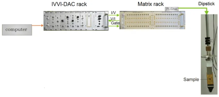
Figure17: A schematic representation of the experimental set-up. Shown are the
IVVI-DAC rack, Matrix rack and the dipstick that will be dipped in a liquid helium dewar at 4.2 K.
4.2 s e t-u p
Figure 17 shows a schematic of the experimental set-up. The PCB with the bonded sample is clamped to the dipstick’s electrical connector and covered with a can that shields the sample from external electro-magnetic fields. The connected and shielded
[image:31.595.132.492.458.618.2]24 m e a s u r e m e n t s e t-u p
sample is dipped into a liquid helium dewar to reach 4.2 K. The sample is, through the PCB and the dipstick connected, to the Matrix rack. From here MCX-MCX wires are used to connect the matrix rack to different modules in the IVVI rack. This rack contains digital to analog converters (DACs) controlled by the computer, measure-ment and conversion modules. The source and drain are connected to the conversion and measurement module of which the voltage is linked to one of the DACs and the current output is measured using a Keithley 2000 multimeter. The DACs have
a range of −2 V to 2 V. To be able to reach higher voltages 5X amplifiers are used.
These are directly linked to the different gates of the devices so that the desired volt-ages can be applied and swept. The sources are connected to a dual V/I source which has a very low noise output. To be able to do this, the output voltage is limited to a
range of −200 to 200 mV, which falls withing the interesting range when analyzing
quantum dots. The current measurement unit used is optimized to only send a low amount of energy to the sample when measuring. This is crucial since the devices we make are very sensitive to small shocks. This unit will also amplify the output current, allowing us to measure relatively low signals. Unfortunately, this module in not optimized for its output resistance. Therefore, when changing the amplification, the current that is measured will change as well. Due to this the measurements done throughout this thesis do not give quantitative but qualitative information. For the study done in this thesis, this is sufficient since the device behaviour is more crucial than the absolute values of the current.
4.3 h e l i o x
As mentioned, a dipstick in a helium dewar is used to measure the devices at 4.2 K. However, to obtain more accurate results due to a reduction in the thermal energy of the QD, another machine needs to be used. To obtain some of the results in this thesis I measured the device properties in the Oxford heliox helium3 fridge, which is capable of reaching temperatures below 300mK. The machine uses helium 3 and a sorption pump. The sorption pump is used to pump helium 3 at high speeds allowing it to be used to reach the before mentioned temperatures through evaporation cooling. The main downside of the system is that there is no continuous flow of helium 3. This helium needs to be recondensed after all the helium 3 is
pumped. This so called holding time varies between 3−10 hours. Unfortunately,
5
R E S U LT S A N D D I S C U S S I O N
The results of electronic transport measurements and charge sensing, of a few se-lected devices are presented in this chapter. They will be discussed in the same order as in chapter 3: palladium, titanium, titanium-palladium and hafnium oxide. From these results of each of these devices are discussed.
5.1 pa l l a d i u m
(A)
Le
Lh SET SHT
BLe
BLh BRh
BRe
(B)
Figure18: Palladium top gate device electron turn-on and pinch-off curves. (A) The
blue turn-on curve is obtained by sweeping the lead and barriers on the electron side. The pinch-off curves of the left and right barrier at the elec-tron side are shown using the orange and green curves. These measure-ments are done with a source drain bias of 1 mV at a temperature of 4.2 K. All other metal contacts are at 0 V. (B) shows a schematic of the device that is colour coded to link the curves to the different parts of the device.
26 r e s u lt s a n d d i s c u s s i o n
In this section the measurement results obtained from the palladium-gate devices are presented and discussed. This is first done with the single-electron transistor of one device, after which the single-hole transistor of another device is analyzed. It was not possible to operate both within one device.
5.1.1 Electrons
The turn-on and pinch-off curves of a self-made single-electron transistor (SET) is presented in figure 18. It shows that the SET turns on in between 2.5 and 3 V (blue curve in the graph). At these gate voltages, a two-dimensional electron gas (2DEG) is accumulated underneath the electron lead gate (Le) and the electron barriers (BLe, BRe). The pinch-off curves (indicated in orange for the left and green for the right barrier) show that this 2DEG can be fully depleted underneath the barriers by putting them below 1 V. By locally depleting the 2DEG, tunable tunnel barriers can be formed underneath the barrier gates. These barriers tunnel-couple the formed island to the source and drain. Therefore, a quantum dot (QD) is formed (see chapter 2.1). In the same figure, the pinch-off curve is not smooth but contains peaks. These peaks indicate the presence of charge traps or dangling bonds underneath the barriers, see section 2.7.
When tuning this device by varying its lead and barrier gate voltages, it is possible to obtain the gate-space shown in figure 19(A). A gate-space is a two-dimensional map of the Coulomb peaks measured through the quantum dot at different gate voltage combinations, see 2.3. It shows different periodic oscillations or Coulomb peaks. The diagonal oscillations give an indication of an intentional quantum dot in between the barriers and under the lead gate (orange circle in the schematic). However, there are also horizontal oscillations that are only coupled to the barriers. This indicates the ex-istence of a second, unintentional QD, underneath the barriers. A bias spectroscopy along the black line is shown in figure 19(B). This spectroscopy is taken such that most of the measurement is done in between the oscillations of the unintentional QD, reducing the influence of this QD on the measurement. This bias-spectroscopy shows differently sized diamonds, showing that the influence of the unintentional QD is not entirely circumvented.
5.1.2 Holes
From the pinch-off graphs presented in figure 20, it can be observed that, even when the lead gate is at 0 V, the source and drain are connected. This indicates that, even though holes have not been accumulated, an unintentional two-dimensional hole gas (2DHG) is present. The theory is, that this unintentional 2DHG results from negative
charges formed at the Al2O3-SiO2 interface, which accumulates holes at the Si-SiO2
5.1 pa l l a d i u m 27 1500 1400 1300 1200 1100 V BLe , V BR e
, (mV
)
VLe (mV)
2500 2750 3000 3250
0.0 -1.6 -3.2 -4.8 -6.4 log 10 (I SD e
) (nA
) (A) V SD (mV )
VLe (mV)
log
10
(dI/dV
) (e
2/h) 10
5
0
-5
-10 2700 2900 3100 0.0 -1.0 -2.0 -3.0 -4.0 (B) Le Lh SET SHT BLe BLh BRh BRe (C) Le Lh SET SHT BLe BLh BRh BRe (D)
Figure19: Gate-space and bias-spectroscopy of the single-electron transistor using
palladium gates. The gate-space in (A) is taken by plotting the two bar-riers vs the lead gate voltage, while the source-drain voltage is kept at 1 mV. The bias-spectroscopy in (B) shows the logarithm of the differential current in colour. The source-drain voltage is plotted against the lead gate voltage taken along the black line in (A)(VBLe=VBRe=1225 mV), Coulomb diamonds are shown. Both measurements are done with the hole gates at 0 V and a temperature of 4.2 K. (C) and (D) show schematics of the de-vice. The gate voltage of the yellow section is plotted on the x and the blue on the y axis. The orange circle indicates the position of the intentional quantum dot.
By confining an island using all metal gates (leads and barriers), a depletion dot can be made in the center of the device (as illustrated in figure 21(C)). Figure 21(A) shows a gate-space where the two left barriers are plotted against the two right bar-riers. The diagonal Coulomb oscillations indicate the formation of an intentional QD. Figure 21(B), shows a bias spectroscopy obtained by sweeping along the black line indicated in (A). Coulomb diamonds are clearly visible showing that a depletion single-hole transistor (SHT) can be formed. However, this QD can not be formed in the indented location, making it more difficult to be formed together with an SET, since turning on this SET depletes the 2DHG that is used to form the island.
28 r e s u lt s a n d d i s c u s s i o n
I
SDh
(nA
)
3.0
2.0
1.0
0.0 1.5
0.5 2.5 3.5
-400 -200 0 200 400 600 VBLe, VBLh (mV)
(A)
I
SDh
(nA
)
3.0
2.0
1.0
0.0 1.5
0.5 2.5 3.5
-400 -200 0 200 400 600 VBRe, VBRh (mV)
(B)
Le
Lh SET SHT
BLe
BLh BRh BRe
(C)
Le
Lh
SET SHT
BLe
BLh BRh BRe
(D)
Figure20: Pinch-off curves at the hole side, indicating the presence of the
5.1 pa l l a d i u m 29 200 100 0 -100 V BR e , V BR h (mV )
VBLe, VBLh (mV)
-200 -100 0 100
0.8 0.2 I SDh (nA ) -200 200 0.4 0.6 0 (A) V SDh (mV ) 10 5 0 -5 -10
VBRe, VBRh (mV)
0 50 100 150 200 250 300 350
dI/dV (e
2/h) 0.0105 0.0075 0.0045 0.0015 (B) Le Lh SET SHT BLe BLh BRh BRe (C) Le Lh SET SHT BLe BLh BRh BRe (d)
Figure21: Gate-space and bias-spectroscopy of the depletion single-hole transistor for
30 r e s u lt s a n d d i s c u s s i o n
Hole Device I
(A)
Electron Device I
(B) Device II
(C)
Device II
(D)
Le
Lh SET SHT
BLe
BLh BRh
BRe
(E)
Le
Lh
SET SHT
BLe
BLh BRh
BRe
(F)
Figure22: Titanium devices turn-on curves and unintentional 2DHG check. (A) and
5.2 t i ta n i u m 31
5.2 t i ta n i u m
In this section, the measurement results of two different titanium gate based devices are compared. These results highlight the inconsistent behaviour within similarly fabricated devices.
Figure 22 shows the turn-on of both hole and electron sides of the devices discussed. During turn-on measurements, the hole and electron turn-on curves are measured simultaneously. For example, while the electron lead and barriers are being swept
from 0 to 2 V, the hole lead and barriers are being swept from 0 to −2 V. Measuring
turn-on in this fashion is known as global turn-on. The peaks (oscillations) that can be observed in the electron turn-on curve of device I, show that there are defects
at the Si-SiO2 interface. However, they can be anywhere underneath the lead and
are possibly outside of the quantum dot formation regime of the device. The small plateau that can be seen on the hole side indicates a small amount of unintentional 2DHG since this plateau is present before lead induced turn-on. The hole side of the second device also shows the unintentional 2DHG. This can be observed from the orange curve: even when the lead gate is at 0 V, hole current can flow between the source and drain contacts. Therefore, the unintentional 2DHG is present in both devices.
When comparing the plots of the two devices, the first thing that we notice is the difference in current when the device is in turn-on. For device I it is a lot higher than for device II. This can be understood when looking at the set-up and changes made to the gain factors between measurements resulting in qualitatively instead of quantita-tive data (see chapter 4). The second difference we observe by looking at the turn-on
voltage on the hole side. For device I, turn-on happens at approximately−1.5 V, while
for device II this happens at approximately −2.5 V. This is most likely caused by a
higher number of defects in device II, indicating the more ideal behaviour of device I.
32 r e s u lt s a n d d i s c u s s i o n
device, the electron side is maintained at its turn-on voltages and vice verse. This is important as to not change the device behaviour when attempting charge sensing. During charge sensing, both devices need to be operated.
Hole Device I V BLh , V BR h (mV ) -450 -500 -550 -600 -650 -700 -750
VLh (mV)
I
SDh
(nA
)
-2500 -2400 -2300 -2200 -2100
0.72 0.56 0.40 0.24 0.8 (A) Electron Device I V BLe
, V
BR
e
(mV
)
VLe (mV)
I SD e (nA ) 1400 1350 1300 1250 1200 1150
1100 2100 2200 2300 2400 2500
0.8 0.6 0.4 0.2 0 (B) Device II V BLh , V BR h (mV ) -1000 -1050 -1100 -1150 -1200
-4000 -3800 -3600 -3400 -3200 -3000
VLh (mV)
0.048 0.036 0.024 0.012 0.00 I SDh (nA ) (C) Device II 1000 950 900 850 800
3000 3200 3400 3600 3800 4000
V BLe , V BR e (mV )
VLe (mV)
I SD e (nA ) 0.12 0.00 0.04 0.08 (D) Le Lh SET SHT BLe BLh BRh BRe (E) Le Lh SET SHT BLe BLh BRh BRe (F)
Figure23: Gate-spaces of the hole and electron side of both titanium gate based
de-vices. (A) and (C) show the Coulomb peaks for both SHTs when plotting the barriers vs the lead. The electron side of the devices are kept at turn-on (BLe=BRe=1.2 V and Le=2 V for device I and BLe=BRe=1 V and Le=4 V for device II). (B) and (D) show the same for the electron side. During
these measurements, the hole side is kept at turn-on (BLh=BRh=−600 mV
and Le=−2 V for device I and BLh=BRh=−1.1 V and Lh=−4 V for device
5.2 t i ta n i u m 33 Hole Device I V Lh (mV )
VLe (mV)
dI/dV (e
2/h) -2000 -2100 -2200 -2300 -2400 -2500 -2600
2000 2100 2200 2300 2400 2500 2600 2.0 1.5 1.0 0.5 0 x10-4 (A) Electron Device I V Lh (mV )
VLe (mV)
dI/dV (e
2/h) -2000 -2100 -2200 -2300 -2400 -2500 -2600
2000 2100 2200 2300 2400 2500 2600 6.4 4.8 3.2 1.6 0 x10-6 (B)
Device II Device II
V
Lh
(mV
)
dI/dV (e
2/h)
dI/dV (e
2/h) -3500 -3600 -3700 -3800 -3900
-4000 3200 3400 3600 3800 4000
x10-4 x10⁻⁴
2.8 2.4 2.0 1.6 1.2 0.8 0.4 0.0
VLe (mV)
V Lh (mV ) -3500 -3600 -3700 -3800 -3900
-4000 3200 3400 3600 3800 4000
VLe (mV)
0.0 0.8 1.6 2.4 3.2 4.0 4.8 (C) (D) Le Lh SET SHT BLe BLh BRh BRe (E)
Figure24: Passive sensing measurements for device I and II.The gates are swept
along the black lines in figure 23. (A) and (B) show the results of
34 r e s u lt s a n d d i s c u s s i o n
Since both the electron and hole side of these devices allow for the formation of intentional quantum dots, the first passive charge sensing experiment is attempted. The plots in figure 24 show that the oscillations of both the electron and hole side can be observed in the separate graphs. However, even though the two devices are similar, in device I the Coulomb peaks of the SHT are observed again at the electron side while this is not the case for device II. This could be caused by the noisier behaviour of device II that is observed in the previous measurements. However, since these charge sensing results seem different from figure 3(B) (section 2.5), we are not certain whether this result originates from capacitive coupling between the SET and SHT or something else. It is also possible that the signal is caused by other phenomena such as leakage. Therefore, for device I, further analysis is done using active sensing.
Electron Hole V BLh , V BR h (mV ) -560 -580 -600 -620 -640
-2600 -2550 -2200
VLh (mV)
V BLh , V BR h (mV ) -560 -580 -600 -620 -640
-2600 -2550 -2200
VLh (mV) x10-4 3.2 2.4 1.6 0.8 0 -0.8 -1.6 -2.4
dI/dV (e
2/h) x10-4 9.0 7.5 6.0 4.5 3.0 1.5
dI/dV (e
2/h) (A) Electron Hole V BR h (mV )
-2600 -2550 -2500
VLh (mV) -2600 -2550 -2500VLh (mV) 200 100 -200 -100 0 V BR h (mV ) 200 100 -200 -100 0
dI/dV (e
2/h) x10-4 3.5 x10⁻⁴ 3.0 2.5 2.0 1.5 1.0 0.5 0.0 0.06 0.04 0.02 0.00 -0.02 -0.04 -0.06
dI/dV (e
2/h) N N-1 N-2 N-3 N-4 (B) Le Lh SET SHT BLe BLh BRh BRe (C) Le Lh SET SHT BLe BLh BRh BRe (D)
Figure25: Active charge sensing of device I. (A) The differential current of the
elec-tron (left) and hole (right) side while sweeping through the oscillations of the hole side, and actively sensing with the SET lead at 2380 mV and elec-tron barriers at 1175 mV. (B) Same as in (A), except that BRe is swept below
pinch-off and BLe is kept constant at−550 mV. The temperature is 4.2 K
5.3 t i ta n i u m-pa l l a d i u m 35
Passive sensing indicates that charge sensing might be possible in device I. Therefore, we attempt active sensing of hole tunneling using the SET. The two images in figure 25 A show that the gate-space obtained from measuring the SHT is copied onto the SET. The main measurement to determine whether these sensing events are due to leakage or capacitive coupling is to do charge sensing past the limit of direct trans-port of the SHT. The result of this measurement is shown in figure 25(B). Here one of the barriers is swept well above its pinch-off voltage. The SHT no longer allows direct transport. However, we still observer regularly-spaced oscillations at the SET side. This shows a system which allows measurements of the energy levels of the hole QD, past its direct transport regime. This brings us one step closer to achieving the single hole regime required to make a hole qubit.
From−650 mV till−630 mV on the barriers in (A), a regime acting different from
the rest of the system is observed. This region, also observed from−300 mV till−100
mV in (B), originates from the sweep direction of the measurement. Every measure-ment is taken from the bottom to the top of the figure. Every time the system has to recalibrate the perfectACvalue of the system, see equation 8 and 9. This initialization
of the feedback loop results in these different regimes.
Even though the results obtained indicate charge sensing, it should be very difficult to achieve this at 4.2 K. At this high temperature, the trans-conductance of the Coulomb peaks should be low, resulting in a low signal. Therefore, to make a conclusive state-ment it is necessary to reproduce these results. This has not succeeded during the project. Therefore, an attempt is made to increase the sensitivity by removing the unintentional 2DHG. Removing the 2DHG will lead to a lower self capacitance of the hole QD. This will increase the relative coupling between the QD and the sensor, resulting in a higher sensitivity (see section 2.5). For these devices, UV-ozone could not be used to remove the 2DHG since this treatment oxidizes the titanium gates.
5.3 t i ta n i u m-pa l l a d i u m
For the device discussed in this section, a 1 nm thick titanium sticking layer is used to increase the fabrication yield of devices made using palladium gates. This is done to allow for UV-ozone treatment without oxidizing the metal gates. Therefore, we should be able to remove the undesirable 2DHG using this treatment. First, the 4.2 K measurements before and after UV-ozone are compared to observe whether the removal of the 2DHG was possible. Afterwards, measurements are done at 440 mK to attempt charge sensing.
5.3.1 Dipstick measurements
In this section, the 4.2 K measurements of one of the devices fabricated using titanium-palladium gates are shown. The influence of UV-ozone treatment is analyzed by com-paring the device behaviour before and after treatment.
36 r e s u lt s a n d d i s c u s s i o n
of (A) before and (B) after the treatment, has been reduced from 2.5 to 2 V. This is the first indication that the 2DHG could have been removed. The voltage needed to deplete this positive charge at the interface is no longer required. However, we also see that more, smaller, oscillations are seemingly present in the curve after the treatment. This indicates an increase in the number of defects in the system. These
are most likely present at the Si-SiO2 interface since they have a strong influence on
the electronic transport near this interface. Whether this results in an increase of unintentional QD can be seen from the pinch-off curves, since a defect only becomes an unintentional QD when tunnel barriers are formed around it. This is indicated by the green and orange curves. It is obvious that the number of oscillations during pinch-off has increased. These extra defects are likely to form unintentional quantum dots, reducing the quality of the device. However, since pinch-off can be achieved, we should be able to form intentional quantum dots using these barriers. It has not been checked whether the electron side of the device could turn-on using only the lead since presence of an unintentional 2DEG is unlikely.
No Treatment
(A)
UV-ozone
(B)
Le
Lh SET SHT
BLe
BLh BRh
BRe
(C)
Figure26: Titanium-palladium gate device. SET turn-on and pinch-off curves before
5.3 t i ta n i u m-pa l l a d i u m 37
The presence of an unintentional 2DHG in this device is checked in figure27. Looking
at the hole side of the device, we observe that before the treatment (A), the lead gate is not capable of turning-off the device, clearly showing the presence of the 2DHG. By comparing the 2DHG behaviour of the palladium and the titanium gate based devices, it is clear that the 2DHG has a higher influence on the turn-on behaviour the palladium devices. After UV-ozone (B), the turn-on with all gates and with the lead are almost exactly the same. Hence, the unintentional 2DHG has been removed. Since the 2DHG has been removed, the pinch-off behaviour of the hole side of the device needs to be analyzed.
No Treatment
(A)
UV-ozone
(B)
Le
Lh
SET SHT
BLe
BLh BRh
BRe
(C)
Figure27: Titanium-Palladium gate device SHT turn-on with all gates and only lead
38 r e s u lt s a n d d i s c u s s i o n
The pinch-off curves in figure 28 show that for the hole side, the amount of uninten-tional oscillations after the treatment (B) increases. However, the increase is smaller than at the electron side. This could be due to the defects present being more sus-ceptible to electrons. It is also possible that the statistical nature of such reactions resulted in less charge defects underneath the barriers on the hole side.
No Treatment
(A)
UV-ozone
(B)
Le
Lh SET SHT
BLe
BLh BRh
BRe
(C)
Figure28: Titanium-Palladium gate device. SHT pinch-off behaviour before (A) and
after UV-ozone treatment (B). (A) shows pinch off with the left barrier in blue and the right barrier in orange before UV-ozone. (B) shows the same after UV-ozone treatment. All gates on the hole side that are not being
swept are kept at−1 V and−2 V for (A) and (B), respectively. The electron
gates are kept at 3 V for both measurements. The source-drain voltages are kept at 1 mV and the temperature is 4.2 K. (C) shows a schematic of the device. The gates that are being swept are indicated using corresponding colours.
When looking at the data obtained before and after UV-ozone treatment, it seems like this treatment does the opposite of hydrogen annealing. Where annealing reduces
the amount of defect at the Si-SiO2 interface, UV-ozone increases this. At the same
time, annealing induces the negative charge at the SiO2-Al2O3 interface, while
UV-ozone removes these negative charges. There is a trade-off between the unintentional
2DHG and the number of charge defects at the Si-SiO2 interface that could result
5.3 t i ta n i u m-pa l l a d i u m 39 SiO2 Intrinsic Si Al2O3 SiO2 Intrinsic Si Al2O3
x x x x x x x x x x x x x x x x x x x x SiO2
Intrinsic Si Al2O3 + + + + + + + + + + + + + + + + + -Annealing SiO2 Intrinsic Si Al2O3 SiO2 Intrinsic Si Al2O3
x + x + x x + x x x + x x + x x + + x - - - - - - -
UV/Ozone x charge defect
+ positive charge - negative charge
No treatment
Figure29: Schematic showing the effect of annealing and UV-ozone on the devices. In
the left schematic there are a lot of charge defects at the Si-SiO2 interface,
indicated by the red crosses. In the middle image, these charge defects have been removed using hydrogen annealing. However, this treatment has introduced a negative charge at the SiO2-Al2O3interface, inducing an
unintentional 2DHG at the Si-SiO2 interface as indicated by the plus and
minus signs. On the right image, some of these negative charges have been removed using UV-ozone. However, some of the charge defects have been reintroduced.
5.3.2 Heliox measurements
The turn-on and pinch-off curves of the titanium-palladium device at 440 mK are presented in figure 30. When comparing to the 4.2 K measurements, we observe
that the turn-on voltages have increased to 3 V for the electron side (B) and −3 V
for the holes side (A). This indicates that it has become more difficult to accumulate electrons and holes underneath the top gates. It is also apparent that the number of oscillations in the turn-on curves have increased. Both correspond to an increase in the number of charge traps in the system. Since the energy levels corresponding to the charge traps and the quantum dots are less thermally broadened, more of them can be measured since there are less overlapping states in the system. Measurements at colder temperatures do not only increase the sensitivity of the device, it also shows more details. A device with a lot of impurities, as the one used here, can show even worse behaviour than at 4.2 K. Looking at the pinch-off curves indicated in green and orange, we note that pinch-off is possible at the hole side, even though there are a lot of oscillations. However, we observe that pinch-off is not properly happening at the electron side. Only a large number of unintentional QD oscillations are observed. Therefore, an attempt is made to improve pinch-off.
40 r e s u lt s a n d d i s c u s s i o n
(A) (B)
Le
Lh SET SHT
BLe
BLh BRh
BRe
(C)
Le
Lh SET SHT
BLe
BLh BRh
BRe
(D)
Figure30: Titanium-palladium device results at 440 mK. (A) turn-on (blue), pinch-off
using the left barrier (orange) and pinch-off using the right barrier (green) for the hole side of the device. (B) electron turn-on and pinch-off of both barriers using the same colour scheme. Global turn-on is measured, thus the hole and electron sides were measured at the same time. During the pinch-off measurements, the other gates were at their respective turn-on
(−3V for the hole and 3 V for the electron side). Once again 1 mV is used
as the source-drain bias. (C) and (D) show schematics of the device. The gates that are being swept are indicated using corresponding colours. (C) relates to (A), and (D) relates to (B).