Shear Fracture Behavior on Ball Grid Arrayed Tin–Silver–Copper
Solder/Pure Copper Pad Joint Interface
Kunihiro Noguchi
1, Yu¯ya Endou
2;*, Isao Shimizu
3and Yasuhide Ohno
3 1Department of Mechanical System, Kumamoto Technical College, Kumamoto 862-0938, Japan 2Graduate School of Science and Technology, Kumamoto University, Kumamoto 862-0862, Japan
3Department of Materials Science and Engineering, Faculty of Engineering, Kumamoto University, Kumamoto 860-0862, Japan Shear strength of Sn–0.39 mass%–3.9 mass%Ag–0.5 mass%Cu lead free solder joint interface on non-resist pure Cu pad were measured to evaluate the true joint strength. Shear test was carried out under the shear speed,Vs¼0:14mm/s and the shear height,Z¼0mmfrom the non-resist substrate surface. Shear fracture generated and propagated complicatedly on the joint interface. The shear strength using the non-non-resist pure Cu pad was lower than that using the FR-4 print board. The reaction layer was composed of Cu5:6Sn and Cu6Sn5intermetallic compound with column shape on the joint interface. Reaction layer thickness,t, column space,sand column width,whave been investigated to analyze the layer structure morphology. Silver composition in the solder influenced on shear strength but not on reaction layer structure morphology. Shear crack propagated intricately in the solder side and the reaction layer side. Shear fracture had the ductile deformation area of the solder and the brittle fracture area of the intermetallic compound.
(Received May 13, 2005; Accepted September 20, 2005; Published November 15, 2005)
Keywords: tin-lead-silver ball, pure copper pad, reflow process, intermetallic compound, shear strength
1. Introduction
Semiconductor devices for cell phone, personal computer, medical electronics and so on have been demanded to be more integrated, smaller and thinner than conventional ones. Ball Grid Array (BGA) technique has been applied in many IC products since BGA technique can make IC device more integrated comparing with Quad Flatpack Package (QFP) technique. BGA technique is a joint process which solder balls are arranged at Cu electrodes on a print board and heated in a reflow apparatus after setting IC chips on solder balls.1–4) Shear test and pull test have been carried out to investigate the joint interface strength.5–8)However, true joint strength obtained by these conventional tests using print board cannot be evaluated correctly because the fracture occurs on only solders side, not on joint interface. Commer-cial print board is covered with resist layer that has about 20mmin thickness except Cu electrode. The joint interface between the solder and the electrode locates under the resist layer. The shear tool hits just solder side as shown in Fig. 1 and the shear strength is reflected from the solder mechanical property. Though pull test is a major method to estimate joint interface strength, this test is acquired the specific tool to grab and pull the minute solder ball. Furthermore, pull test could not be realistic method because solder ball tends to become smaller and smaller as IC device is more integrated. Sn–Ag– Cu ternary systematic solder alloys have been focused as a lead-free solder alloy from the viewpoint of environmental issue in spite of their higher melting points with that of eutectic Sn–Pb alloy. Various mechanical and physical properties of Sn–3 mass%Ag–0.5 mass%Cu solder alloy/ electrode on the print board joint have been studied by shear test, pull test, bending test, thermal fatigue test and so on.9–14) Recently, the soldering on pure Cu substrates has been focused and tried because the Under Bump Metallizing
(UBM) treatment of electro less Ni–P plating and Au vaporization on pure Cu substrates has been increased the cost of IC device production.15) Furthermore, Cu cored technique in solder ball has been researched from the aspect of the ball strength and electric conductibility.16)Therefore, it is important to investigate the interface reaction, mechanical strength and fracture behavior between the lead-free solder and pure Cu substrates. In this study, shear strength of Sn– 0.39–3.9 mass%Ag–0.5 mass%Cu lead free solder joint inter-face on non-resist pure Cu pad were measured to evaluate the true joint strength.
2. Experimental Procedure
Table 1 shows chemical compositions of Sn–Ag–Cu solder ball used in this study. The diameter of the balls was 400mmin average. Nittetsu Micro Metal Co., Ltd. supplied the balls. Each solder/pure Cu (99.99%) pad joint is described as Ag contents in this paper. Figures 2(a) and (b) show the preparation of pure Cu pad by mechanical grinding. The stainless steel tube with 400mmin internal-diameter was fixed to the chuck of table drilling machine. The tube was forced on the pure Cu surface as revolving under the condition of 1730-rpm rotation and 0.1 N loads. The diameter of the pad was approximately 400mm in average. There is apparently no crack on the pad by grinding as indicated in Fig. 2(c). Figure 3(a) shows the reflow profile. The solder balls were put on each Cu pad with a tweezers after the commercial flux liquid was applied on the Cu pads. The reflow was performed in nitrogen atmosphere with RS-2 type reflow simulator (Marcom Co., Ltd.). FR-4 (square 40
40mm2, 336 Cu pads) was selected as the testing board material to compare with pure Cu pad since it is one of the commonly used substrates for printed circuit fabrication. The Cu electrodes on FR-4 were covered with 4mmthick Ni–P electroless-plating layer and Au vaporize layer with approx-imately 0.1mmon Ni–P electroless-plating layer. The shear *Graduate Student, Kumamoto University
test was carried out as follows. The shear height,Zwas set at 0mmfrom pure Cu substrate surface as shown in Fig. 3(b). The shear speed,Vswas 0.14 mm/s. The shear value of each
specimen was estimated by the average of at least 10 times trials. The observation of the interface reaction layer and the shear fracture was performed with an optical microscopy and a scanning electron microscopy (SEM, accelerative voltage; 20 kV). The joints after reflow were put into the beaker hold the etching liquid (HNO3:Ethyl. alcohol = 1:3) and were
[image:2.595.129.468.80.217.2]vibrated with the ultra sonic wave apparatus to eliminate only solder for approximately 10 min. The fracture morphology of the reaction layer after shear test was surveyed with SEM. Transmission electron microscopy (TEM, accelerative volt-age; 200 kV) was used to analyze the reaction layer on the joint interface.
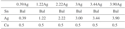
Table 1 Chemical compositions of Sn–Ag–Cu solder ball used in this study (mass%). Ball diameter; 400mm.
0.39Ag 1.22Ag 2.22Ag 3Ag 3.44Ag 3.90Ag
Sn Bal Bal Bal Bal Bal Bal
Ag 0.39 1.22 2.22 3.00 3.44 3.90
Cu 0.5 0.5 0.5 0.5 0.5 0.5
Pure Cu
0.1 N 1730 rpm
Steel cylinder
φ 400 µm
(a)
Cu pad diameter (φ 400 µm)Pure Cu
(b)
(c)
Cu pad surface200 µm
Fig. 2 Schematic illustration of preparation of pure Cu pad by mechanical grinding; grinding process (a), Cu pad surface after mechanical grinding (b) and optical micrograph of pure Cu pad surface (c).
132 K/min 240 K/min
Temperature / K
523K
423K
0.5min
1 min
200K/min
293K
Solder ball
Shear tool
Cu pad
(b)
(a)
Time / min
Fig. 3 Reflow profile of reflow process (a) and schematic illustration of shear test (Z¼0mm) using pure Cu pad (b).
Resist layer
Solder ball
20 µm Shear
tool
100 µm
Shear direction
Solder Cu
Glass epoxy substrate
Resist layer
(a)
(b)
[image:2.595.130.468.252.427.2] [image:2.595.311.539.479.755.2] [image:2.595.45.291.501.559.2]3. Experimental Results and Discussion
[image:3.595.128.469.73.230.2]3.1 Microstructure and morphology of as-reflowed re-action layer
Figure 4 shows optical micrographs of 3Ag joint cross section. Solder ball was bonded on Cu pad without spreading to the other area except the pad area by wet ability of solder as seen in Fig. 4(a). The solder ball height after the reflow was about 300mm and the ball shape was the same independently of the substrates. The reaction layer with column shape forms on the joint interface. It is noted that the reaction layer generates on the joint interface and grows in random direction. The reaction layer was Cu6Sn5
interme-tallic compound as explained in Paragraph 3.4. When the commercial print board with the normal electrode (Cu/Ni–P electroless plating/Au vaporizing layer) is used, (Cu,Ni)6Sn5
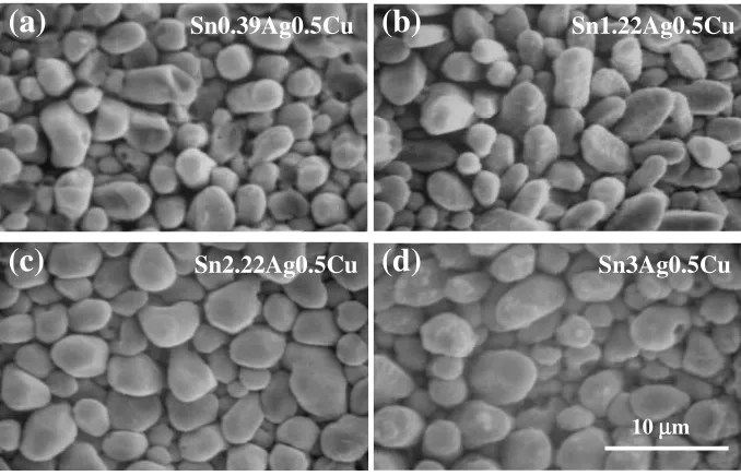
forms on the joint interface between Sn–Ag–Cu solder and electrode.17–19) However, very rough reaction layer with characteristic shape was observed in case of using pure Cu pad without UBM layers. Figures 5(a) to (d) show SEM micrographs of inetrmetallic compound on joint interface of
0.39–3Ag joints, respectively. The solder area is utterly excluded by etching and three-dimensional observation of column reaction layer can be possible. The column reaction layer randomly forms and grows almost linearly from the joint interface to the solder side. Nearly same structure morphology was seen regardless of Ag contents in SEM scale. Figure 6 shows optical micrographs of 3.44Ag joint
Cu
6Sn
5Solder side
Cu pad
5
µ
m
Cu pad
Solder ball
100
µ
m
(a)
(b)
Fig. 4 Cross sectional optical micrographs of joint (a) and joint interface (b) of Sn3 mass%Ag0.5 mass%Cu solder/pure Cu pad.
Sn0.39Ag0.5Cu
Sn1.22Ag0.5Cu
Sn2.22Ag0.5Cu
Sn3Ag0.5Cu
10 µm
(b)
(a)
(c)
(d)
Fig. 5 SEM micrographs of intermetallic compounds on joint interface of Sn0.39–3 mass%Ag0.5 mass%Cu solder/pure Cu pad (a)–(d), respectively.
Solder side
Cu 10 µm
Space, s
Width, w
Thickness, t
Interface Cu6Sn5
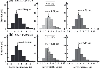
[image:3.595.128.467.269.487.2] [image:3.595.306.547.530.649.2]cross section. In this study, reaction layer thickness, t, column space, s and column width, w was surveyed to analyze the layer structure morphology. Calculating the average of five the thickest columns (peak parts) and five the thinnest layers (valley parts) estimated the reaction layer thickness. Figures 7(a) and (b) show histograms expressed the distribution of t, s and w of 2.22Ag and 3.44Ag joint reaction layer, respectively. Each value N in Fig. 7 expresses the column number calculated from the cross sectional micrographs as shown in Fig. 6. The average oft,sandwis not affected by Ag composition. Other joints had almost the same distribution of t, s and w. These analyzing results support the results of SEM observation (Fig. 5).
[image:4.595.99.497.82.359.2]3.2 Shear strength of joint interface
Figure 8 shows shear test results. The shear strength using the normal print board and of only reaction layer eliminated the solder side by etching is also added in Fig. 8. The circle vacant plots express the shear test result obtained under the shear height,Z¼20mm, from the pure Cu substrate surface. The shear strength using the print board corresponds to that performed underZ¼20mmsituation. Figure 9 shows cross sectional SEM micrograph of shear fracture of 3Ag solder/ pure Cu pad joint in the middle of the shear test at Z ¼20mm. When the shear position is the same and the shear fracture occurs in the solder side, there is no change in the shear strength even if the different substrate was utilized. We reported that the shear strength using the print board was reflected from the solder mechanical property since the fracture occurred on the solder side caused by the resist layer. The closer eutectic composition (Sn–2.73–3.44Ag–0.5Cu) of
the solder has, the finer structure (primary Sn and eutectic structure (Sn/Ag3Sn) is gained20,21)). Therefore, the shear
strength of the joint with near eutectic composition is higher than that with other compositions in case of using the print board. The circle mad plots indicate the shear test results gotten under the shear height, Z¼0mm, from the joint interface. It is clear that the shear strength is lower than that using the print board. Therefore, the shear fracture might occur close to the joint interface (solder/pure Cu pad). It can be thought that the shear fracture progressed complicatedly between the solder side and the reaction layer side. The detailed consideration is described in Paragraph 3.3. Since
40
Fraction (%)
8 60
20
10 12 0
= 5.44 µm
w = 4.21 µm s = 4.44 µm
N = 143
40
Fraction (%
)
0 2 4 6
0 2 4 6
8 60
20
10 12 0
0 1 2 3 4 5 6 7 8 9 10
Layer thickness, t/ µm = 5.00 µm
0 1 2 3 4 5 6 7 8 9 10
Layer width, w/ µm Layer space, s/ µm
w = 4.21 µm s = 4.38 µm
N = 145
(a)
Sn2.22Ag0.5Cu
(b)
Sn3.44Ag0.5Cu
40 60 20 40 60 20 40 60 20 40 60 200 1 2 3 4 5 6 7 8 9 10 0 1 2 3 4 5 6 7 8 9 10
tav
tav
av
av av
av
Fig. 7 Histograms expressed reaction layer morphology, t, w, s of Sn2.22 mass%Ag0.5 mass%Cu (a) and Sn3.44 mass%Ag0.5 mass%Cu (b). 4 6 Shear str ength, F / N 8
FR-4 print board
Z = 0 µm
Ag contents (mass%)
0 1 2 3 4
0 2 Intermetallic compound 4 6 8 0 2
Z = 20 µm
[image:4.595.314.543.417.591.2]the shear curve changes with Ag contents and achieves almost the same behavior comparing to that using the print board, the shear strength might include the solder mechanical property a little. On the contrary, the shear strength of 3.9Ag decreases sharply in comparison with that of other near eutectic solder joints. Figure 10 shows cross sectional SEM micrograph of as-reflowed 3.9Ag joint interface. The needle intermetallic compound can be observed with the column Cu6Sn5 as indicated by the arrow in Fig. 10, though its
number is much fewer than that of the column Cu6Sn5. The
most needle intermetallic compound formed on 3.9Ag joint interface in the other joints. This intermetallic compound had approximately 200mm in length and reached to the half position of the solder ball with no change of its width. The needle intermetallic compound is evidently deferent with column Cu6Sn5 from the point of the size and the shape.
3.9Ag solder contains much more Ag than that in the eutectic solder. It is well known that needle shape Ag3Sn forms on the
joint interface in Sn–Ag–Cu ternary systematic solder/Cu electrode.6) Therefore, brittle Ag3Sn with the needle shape
could become the origin of the shear crack and the shear strength dropped drastically. The triangle plots expresses the
mechanical property of only intermetallic compound sur-veyed by sticking the shear tool extremity into the reaction layer and shearing under the same shear speed. The reaction layer strength is the lowest in other shear test results. Since the reaction layer thickness is about 5mmin average and the contact area with the shear tool is very tiny, these values are not necessarily correct. But the effect of Ag contents on the reaction layer strength itself could be estimated by the shear test. The reaction layer strength is almost constant regardless of Ag contents. It can be thought that Ag contents influences little on reaction layer strength itself.
3.3 Shear fracture behavior
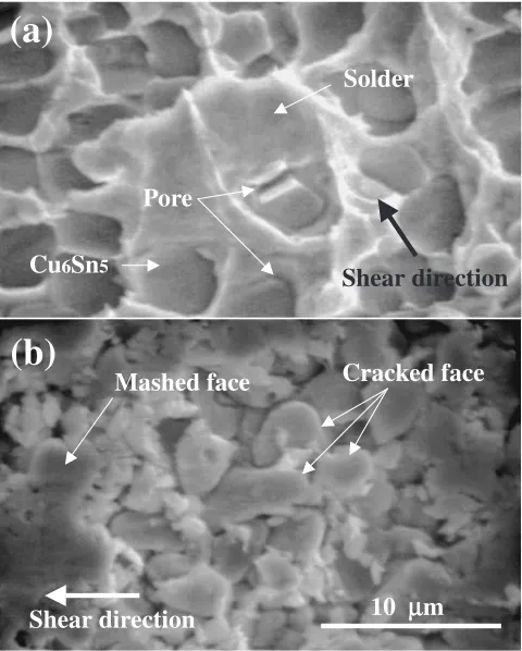
Figures 11(a) and (b) show SEM micrographs of shear fracture face of 3Ag joint interface and of only reaction layer, respectively. The arrows in Fig. 11 are the shear direction. Mixture of ductile deformation area of the solder and brittle deformation area of the intermetallic compound can be seen in Fig. 11(a). The lower shear strength using the pure Cu pad than that using the print board as shown in Fig. 8 was affected by the complex fracture between the solder and the reaction layer. The pore forms at the boundary of the solder [arrows in Fig. 11(a)] and the intermetallic compound as if the solder was stripped from the boundary with the reaction layer. It can be considered that the shear strength is implicated in the mechanical properties of the solder, the reaction layer and the joint force of them. In case of shearing only intermetallic compound, cracked and mashed area is observed as shown in Fig. 11(b). Therefore, Cu6Sn5 might be soft material
un-100 µm Cu pad
Solder ball
Shear direction
Z = 20 µm
Joint interface
Fig. 9 Cross sectional SEM micrograph of shear fracture in the middle of shear test atZ¼20mmfrom Sn3 mass%Ag0.5 mass%Cu/pure Cu pad joint interface.
10
µ
m
Solder
Ag
3Sn
Cu
6Sn
5 [image:5.595.48.289.303.467.2]Cu pad
Fig. 10 Cross sectional SEM micrograph of joint interface of Sn3.9 mass%Ag0.5 mass%Cu/pure Cu pad.
Shear direction
10
µ
m
Solder
Cu
6Sn
5Shear direction
(b)
(a)
Pore
[image:5.595.307.547.447.746.2]Cracked face
Mashed face
expectedly. Figure 12(a) show SEM micrograph of 0.39Ag joint in the middle of the shear test. The shear tool passes close to the joint interface. Figure 12(b) shows SEM micro-graph magnified a frame part in Fig. 12(a). Some ineterme-tallic compound is bent and some is cleaved in two as indicated by the arrows in Fig. 12(b). The fracture face of the solder is so wavy and points out that the ductile deformation of solder occurred. Figures 12(c) and (d) show SEM micro-graphs of shear fracture face of 2.22Ag joint interface in the middle of the shear test. Figure 12(d) shows SEM micro-graph magnified a frame part in Fig. 12(c). It is noteworthy that the upright intermetallic compound is detected without bending and riving though there are many intermetallic compounds with bent and sharply split. These fracture morphology was observed in the other joints. The boundary of the solder and the intermetallic compound might be weak.
3.4 TEM observation of reaction layer
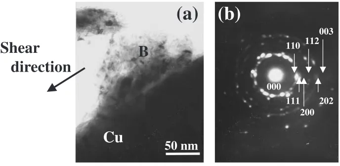
Figure 13(a) shows the schematic illustration of TEM specimen preparation. The shear test was stopped before the fracture was completed. The specimen was fixed with epoxy resin so as not to make the crack progressed more. After slicing the specimen to about 0.5 mm in thickness by micro cutter, both face of specimen was thinned to approximately 0.1 mm by mechanical grinding with SiC emery paper (#1500) and was buff-polished with diamond slurry (particle size; 0.5mm). The specimen was reinforced with two Cu mashes (outer diameter; 3 mm, inner diameter; 1.5 mm) as shown in Fig. 13(b). Furthermore, Argon ion milling thinned the specimen finally for TEM observation. Figure 14(a) shows SEM micrograph magnified edge position of crack in Fig. 13(b). Figures 14(b) and (c) show electron diffraction pattern and TEM bright field image from B area in Fig. 14(a). The column intermetallic compound is regarded as Cu6Sn5
(Hexagonal,a0¼0:42nm,c0¼0:51nm, ASTM 2-0713) by
analyzing electron diffraction patterns as shown in
Fig. 14(b). Figure 15(a) shows TEM bright field image of reaction layer near the shear fracture of 3.44Ag joint. Figure 15(b) shows electron diffraction pattern from B area in Fig. 15(a). Ring patterns with innumerable spots as shown in Fig. 15(b) indicates that the reaction layer nearest to pure Cu pad has very fine grains. By analyzing the electron diffraction patterns and surveying the plane distance, very
(a)
100 µm
Shear direction
Solder
Cu6Sn5
10 µm Solder ball
Cu pad
Cu pad Solder ball
(b)
Shear direction
100 µm 10 µm
Sn0.39Ag0.5Cu
Sn2.22Ag0.5Cu
(c)
(d)
Crack [image:6.595.128.469.73.304.2]Crack Cu6Sn5
Fig. 12 SEM micrographs of shear fracture of Sn0.39 mass%Ag0.5 mass%Cu (a), (b) and Sn2.22 mass%Ag0.5 mass%Cu/pure Cu pad joint interface (c), (d) in the middle of shear test.
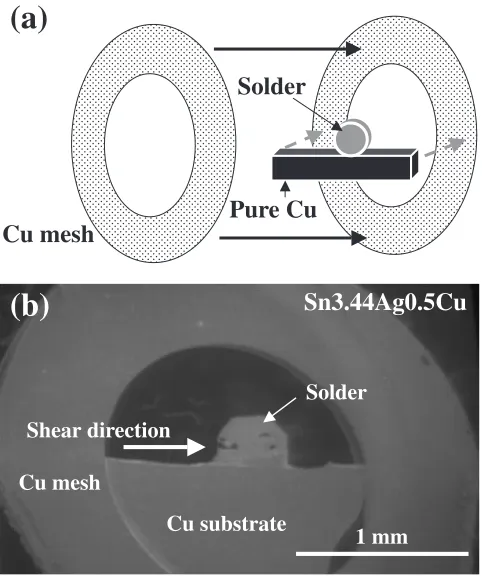
Cu mesh
Cu substrate
Shear direction
Solder
1 mm
Sn3.44Ag0.5Cu
(b)
(a)
Cu mesh
Pure Cu
Solder
[image:6.595.307.548.362.651.2]fine Cu5:6Sn (Tetragonal, P4/n (85),a¼0:37nm,c¼0:36
nm, ASTM 31-487) intermetallic compound formed between Cu6Sn5 and pure Cu pad. The thickness of Cu5:6Sn was
approximately 0.3mm. This phase has never been reported before. Considering the other researchers’ reports,10,13) Cu3Sn intermetallic compound should be observed directly
under Cu6Sn5. But Cu3Sn was not detected in this study. The
existence area of Cu3Sn and its effect on the shear fracture
are under study. From TEM observation of shear fracture face, the shear crack formed and propagated intricately in the solder and two kinds of inetrmetallic compounds (Cu6Sn5
and Cu5:6Sn).
4. Conclusions
Shear strength of Sn–0.39 mass%–3.9 mass%Ag–0.5 mass%Cu lead free solder joint interface on non-resist pure Cu pad were measured to evaluate the true joint strength. The shear test (Vs¼0:14mm/s andZ ¼0mm) was carried out to
investigate the shear fracture behavior. The reaction layer and fracture morphology was observed with optical mi-croscopy, SEM and TEM. The reaction layer morphology, the shear strength and the shear fracture behavior surveyed in the present study are described as follows.
(1) The joint reaction layer formed between the solder and
pure Cu pad was Cu6Sn5with about 5mmin thickness
and Cu5:6Sn with about 0.3mmin thickness.
(2) Cu6Sn5 with column shape grew linearly to the solder
side. Ag contents influenced little on Cu6Sn5
morphol-ogy and distribution.
(3) The shear strength using pure Cu pad was lower than that using the conventional print board.
(4) The shear fracture generated and propagated compli-catedly in the solder, the intermetallic compounds (Cu6Sn5, Cu5:6Sn) and the boundary of them.
REFERENCES
1) K.-L. Lin and Y.-C. Liu: IEEE Trans.22(1999) 568–574. 2) K.-L. Lin and Y.-C. Liu: IEEE Trans.22(1999) 580–585.
3) J. Kloeser, J. K. Heinricht, K. Kutzner, E. Jung, A. Ostmann and H. Reichl: IEEE Trans.21(1998) 41–50.
4) S. Oida, K. Ohmori, S. Sakaguchi and K. Matsushita: Proc. 8th Symposium on ‘‘Microjoining and Assembly Technology in Electron-ics’’, (MATE, Yokohama, 2002) pp. 253–256.
5) N. Torazawa, S. Arai, K. Shimoyama, K. Sasaki and H. Saka: J. Jpn. Inst. Met.66(2002) 1122–1130.
6) T. Nakamori, M. Ikeda, K. Noguchi, I. Shimizu and Y. Ohno: Trans. JIM43(2002) 2130–2136.
7) K. Noguchi, M. Ikeda, I. Shimizu, Y. Kawamura and Y. Ohno: Trans. JIM42(2001) 761–768.
8) K. Noguchi, M. Ikeda, I. Shimizu and Y. Ohno:Proc. The 4th Pacific
(b)
(c)
B // [ 1 2 1 3 ] 0000
0111 1101
200 nm 10 µm
(a)
Sn3.44Ag0.5CuSolder
Cu6Sn5
Cu substrate Solder
B
Interface
[image:7.595.131.469.73.206.2]Shear direction
Fig. 14 SEM micrograph (a), electron diffraction pattern (b) from area B in (a) and TEM field image (c) of Sn3.44 mass%Ag0.5 mass%Cu/pure Cu joint interface in the middle of shear test.
B
Cu
Shear
direction
50 nm
(a)
(b)
000 110
111 200
112
202 003
[image:7.595.126.470.263.431.2]Rim International Conference on Advanced Materials and Processing (PRICM4), (JIM, 2001) pp. 1043–1046.
9) M. Kitajima, T. Shono, T. Ogino, T. Kobayashi, K. Yamazaki and M. Noguchi: J. Inst. Electron. Jissou6(2003) 433–438.
10) C. Yorita, Y. Imamura, Y. Hirohata and K. Asakura: J. Jpn. Inst. Met.5 (2004) 282–287.
11) P. L. Tu and Y. C. Chan: IEEE Trans.23(2000) 750–756.
12) J.-K. Lin, A. D. Silva, D. Frear, Y. Guo, S. Hayes, J.-W. Jan, D. Mitchell, B. Yeung and C. Zhang: IEEE Trans. Electron. Pack. Manuf. 25(2002) 300–306.
13) Y. Nakahara, R. Ninomiya, M. Tagami, M. Sugai and S. Nakata:Proc. 8th Symposium on ‘‘Microjoining and Assembly Technology in Electronics’’, (MATE, Yokohama, 2002) pp. 249–252.
14) T. Kiga, S. Hattori and Y. Iwanabe: J. Inst. Electron. Jissou6(2003) 420–427.
15) T. Nakamori, M. Suenaga, D. Hirakawa, Y. Ohno, T. Hagihara, J. Kagami and T. Takeuchi:Proc. 14th Symposium on ‘‘Microelectronics
(MES, 2004)’’, (2004) pp. 57–60.
16) S. Kiyono, K. Uenishi, K. Kobayashi, I. Shohji and M. Yamamoto: J. Inst. Electron. Jissou2(1999) 298–302.
17) M. Ito, M. Yoshikawa, Y. Nakagawa, G. Katagiri, T. Hiranori, A. Hirose and K. Kobayashi:Proc. 8th Symposium on ‘‘Microjoining and Assembly Technology in Electronics’’, (MATE, 2002) pp. 231–236. 18) T. M. Korhonen, P. Su, S. J. Hong, M. A. Korhonen and C. Y. Li:
J. Electron. Mater.29(2000) 1194–1199.
19) K. Noguchi, T. Nakamori, I. Shimizu and Y. Ohno:Proc. The 10th Symposium on ‘‘Microjoining and Assembly Technology in Electron-ics’’, (MATE, Yokohama, 2004) pp. 319–322.
20) K. Suganuma, K. S. Kin and H. S. Huh:Proc. 2001 Int. Symposium on Microelectronics, (2001) pp. 529–534.