CONVENTIONAL METHODS OF PLASMA ETCHING IN SEMICONDUCTOR
1,*
Neelam Rani,
1, 2
Department of Humanities and Applied Science, YMCA University of Science and Technology,
3
Department of Applied Science and Humanities, PDM College of Engineering, Bahadurgarh, Haryana, India
ARTICLE INFO ABSTRACT
Etch is a process step for
and charged ions and electrons by dissociation and ionization of natural gas. The substrate to be etched is placed is contact with this mixture and etching produce through the synerg
the substrate and directionally impinging ions. In this paper we discussed Properties, different methods and steps of etching for the semiconductor manufacturing process. In this paper we discussed number of advantages and disadvantage
Copyright © 2015 Neelam Rani et al. This is an open access article distributed under the Creative Commons Att distribution, and reproduction in any medium, provided the original work is properly cited.
INTRODUCTION
The concept of plasma in a solid is used to describe by collective response of quasineutral system consisting of free charge carrier of two signs and ionized impurity of two signs to electromagnetic perturbations. The medium for charge carriers in solids is characterized by high value of dielectric constant, which makes it possible to ionize
realize the plasma states even at low temperatures. The ions of this plasma are connected with lattice. The ions and holes move freely over the crystal without violating the neutrality conditions. Each free electron corresponds to positively c and each hole corresponds to a negatively charged. The plasma contains one kind of mobile carriers is called stationary and it is assumed that opposite signs of compensating charge is present. So, other names of intrinsic plasma are “compensated”, “neutral” and “mobile”. In the deposition step, a metal, semiconductor or dielectric film is applied to wafer. A deposition film is masked with a protective film or lithographically patterns. A thin film of polymer is spun into the wafer then irradiated with ultraviolet light through quartz mask with circuit pattern.
*Corresponding author: Neelam Rani,
Department of Humanities and Applied Science, YMCA University of Science and Technology, Faridabad, Haryana, India
ISSN: 0975-833X
Article History:
Received 10th July, 2015 Received in revised form 19th August, 2015
Accepted 05th September, 2015
Published online 31st October, 2015
Key words:
Plasma Ashing, Plasma Etching, Semiconductor, Photolithography.
Citation: Neelam Rani, Manikant Yadav and Mathur, Y. K.
manufacturing process”, International Journal of Current Research
RESEARCH ARTICLE
CONVENTIONAL METHODS OF PLASMA ETCHING IN SEMICONDUCTOR
MANUFACTURING PROCESS
Neelam Rani,
2Manikant Yadav and
3Mathur, Y. K.
Department of Humanities and Applied Science, YMCA University of Science and Technology,
Faridabad, Haryana, India
Department of Applied Science and Humanities, PDM College of Engineering, Bahadurgarh, Haryana, India
ABSTRACT
Etch is a process step for microelectronics industry. Plasma etching form reactive neutral fragments and charged ions and electrons by dissociation and ionization of natural gas. The substrate to be etched is placed is contact with this mixture and etching produce through the synerg
the substrate and directionally impinging ions. In this paper we discussed Properties, different methods and steps of etching for the semiconductor manufacturing process. In this paper we discussed number of advantages and disadvantages of plasma etching.
is an open access article distributed under the Creative Commons Attribution License, which distribution, and reproduction in any medium, provided the original work is properly cited.
The concept of plasma in a solid is used to describe by system consisting of free charge carrier of two signs and ionized impurity of two signs to electromagnetic perturbations. The medium for charge carriers in solids is characterized by high value of dielectric constant, which makes it possible to ionize atoms and to realize the plasma states even at low temperatures. The ions of this plasma are connected with lattice. The ions and holes move freely over the crystal without violating the neutrality conditions. Each free electron corresponds to positively charge and each hole corresponds to a negatively charged. The plasma contains one kind of mobile carriers is called stationary and it is assumed that opposite signs of compensating charge is present. So, other names of intrinsic plasma are In the deposition step, a metal, semiconductor or dielectric film is applied to wafer. A deposition film is masked with a protective film or lithographically patterns. A thin film of polymer is spun into ultraviolet light through quartz
Department of Humanities and Applied Science, YMCA University of Science and Technology, Faridabad, Haryana, India.
The ultraviolet light scissions the po
area so that it can be washed away by a solvent.
then etched by exposure to corrosive dissociated neutral fragments and plasma ions. In the end, remaining photo resist is stripped away or ash by a remote oxygen plasm process is repeated for other circuit levels.
Plasma ashing and plasma etching basically rely on the same principles.
International Journal of Current Research
Vol. 7, Issue, 10, pp.22036-22040, October, 2015
INTERNATIONAL
Neelam Rani, Manikant Yadav and Mathur, Y. K., 2015. “Conventional methods of plasma etching in semiconductor
International Journal of Current Research, 7, (10), 22036-22040.
CONVENTIONAL METHODS OF PLASMA ETCHING IN SEMICONDUCTOR
Y. K.
Department of Humanities and Applied Science, YMCA University of Science and Technology,
Department of Applied Science and Humanities, PDM College of Engineering, Bahadurgarh, Haryana, India
microelectronics industry. Plasma etching form reactive neutral fragments and charged ions and electrons by dissociation and ionization of natural gas. The substrate to be etched is placed is contact with this mixture and etching produce through the synergistic interaction of the substrate and directionally impinging ions. In this paper we discussed Properties, different methods and steps of etching for the semiconductor manufacturing process. In this paper we discussed
ribution License, which permits unrestricted use,
The ultraviolet light scissions the polymer bonds in irradiated area so that it can be washed away by a solvent. The substrate then etched by exposure to corrosive dissociated neutral fragments and plasma ions. In the end, remaining photo resist is stripped away or ash by a remote oxygen plasma. This process is repeated for other circuit levels.
Plasma ashing and plasma etching basically rely on the same
INTERNATIONAL JOURNAL OF CURRENT RESEARCH
Plasma Etching is usually confined to the semiconductor industry and more often than not uses carbon tetrafluoride (with oxygen) as the plasma process gas. Probably the most frequent application is the etching of silicon, silicon oxides, and silicon nitrate as well as glass passivation layers. Failure Analysis of integrated circuits is also an important application of plasma processing. Oxygen gas is used to remove epoxy encapsulates or CF4/02 is used to remove glass filters in the
encapsulates so as to uncover devices which have failed. Inspection by, say, SEM is then possible.
When etching, it should always be remembered that not only the required surface may be removed. The choice of gas is made so that preferential etching of the required surface is attained. Plasma Etching is a chemical process where the RF discharge generates species which react with the material being etched to form a volatile product which is swept away by the gas flow. Since reactive species are being formed the reactant gas is chosen to give the highest concentration of the etching species involved. The need for plasma etching is for advanced IC Fabrication with small geometries requires precise pattern transfer.
Plasma Composition
Typical plasma contains:
Neutral Molecules at a density of 10e16/cm3 Radicals 10e14/cm3 Electrons 10e8/cm3 Positive ions 10e8/cm3
There are a million times more radicals than ions or electrons. Radicals form more easily and their lifetime is much longer. Ions don’t etch, radicals do. Ions affect the process by energetic (physical) bombarding of the surface, influencing the chemical processes of etching. Radicals are responsible for the dry etching process. They are chemically active and react with the surfaces to produce volatile products.
Basics of Plasma Etching
CF4 is inert gas add electron impact to produce fluorine
radicals:
CF4 + e => CF3 + F + 2 e (Dissociative Ionization)
CF4 + e => CF3 + F + e (impact dissociation)
Then chemically form volatile SiF4:
Si + 4F => SiF4 (gas)
CF4 + e- --> CF3 + F e-
F radicals adsorb on silicon surface; SiF4 desorbs and CF3
radicals also adsorb:
CF3 + F => C4 desorbs
The presence of carbon on the surface reduces the amount of fluorine available to etch silicon. Carbon will leave the surface by combining with F reducing fluorine; carbon can remain on the surface forming C-F polymers which in turn inhibits etching. High F/C ratio favors etching. Adding O2 can increase
etch rate and increases selectivity over oxide.
Purpose of etch
• To remove material from areas identified by the lithography process
• Areas of photoresist exposed to light • Developing leaves only these areas open • Etching removes substrate areas not masked
• To create structures for functional use
• To remove oxide layers below features to allow for motion
Lithography provides a method to mask or open up certain areas on a silicon wafer surface. When the resist layer that has been deposited on the substrate is exposed to radiation through a mask, the resist changes chemically. Subsequent development removes the exposed resist, leaving these regions defined, but not permanently changed. The etch process removes the species from the exposed areas, permanently changing the makeup of those areas. Connections to lower layers, subsequent patterning and layering above these areas can define additional functionality in these regions. In MEMS, features that were defined at the top level are sometimes placed on top of a so-called sacrificial oxide layer. Etching provides a method to remove this oxide so that the features above can “move” on the surface. There is no parallel to this in the semiconductor world.
The silicon substrate that makes up a wafer is an insulator, but can be doped with impurities to create conductive species. Removal of certain areas to create transistor structures is common. Silicon dioxide forms on a wafer surface due to the reactive nature of silicon with atmospheric oxygen. It can serve as an effective masking method for the doping process above. In order to create a region of desired conductivity, the SiO2 is
etched from a given area defined by a mask. The doping process that follows occurs only in that area, since the other areas are shielded by the SiO2 that remains in the unexposed
areas. Silicon Nitride is a hard, scratch resistant layer used in place of SiO2. Aluminum is often for wiring and
interconnections in a device, but is often deposited in a bulk process that must later be patterned to create the wires. Tungsten is used as an interconnect between layers of a device, and also requires patterning.
Etch process properties
Any etch process is characterized by certain properties
Etch Rate
• The amount of material removed from the wafer over a defined period of time
Uniformity
• The evenness of the removal over the entire surface of the wafer
Profile
• Isotropic – Etching proceeds at equal rates in both horizontal and vertical direction
• Anisotropic – Etching proceeds faster in one plane than in another
Selectivity
Damage – Any surface or substrate damage acquired from the processing technique
In any etch process; we must look at certain key areas to characterize its performance. The etch rate, often given in angstroms/minute, indicates how quickly the process proceeds. In determining throughput, this is a key indicator. The uniformity of the etch at different sites on the wafer is checked to ensure that all devices on a wafer will be processed in the same way. A non-uniform etch could over etch certain areas of the wafer, removing protective masking or more of a layer than necessary, while leaving other areas correctly processed. In test wafers, measurements are typically made at different points to identify the uniformity.
The profile of the etch process defines what features may be created by a given process. Isotropic etching proceeds in all directions. This is sometimes undesirable if tall, narrow features, such as gratings or combs are desired. Anisotropic etch processes remove more material in one direction, generally in the vertical direction, than in the other. So vertical sidewalls characterize a commonly defined anisotropic etch process.
Etching - Wet and Dry
Wet Etch
Wet etching is the oldest method of material removal still in use. The entire wafer, or often a boatload of wafers, is immersed in a liquid etchant solution, rinsed to remove traces of the etch solution, and dried to remove water.
• Oxidation-reduction equations often define wet etch processes
• Silicon etch with HNO3 & HF
• Si + HNO3 & HF → H2SiF6 + HNO2 + 2H
• Most Wet Etch Processes are Isotropic
• Etch proceeds in both vertical and horizontal direction • Etch mixtures can change the etch rate or profile depending
on silicon crystal orientation
Wet etch processes are typically very selective in nature, which is advantageous in processing and are simpler to carry out t dry etching. Oxidation-reduction chemical equations define many of the reactions that take place. The etchant mix can be altered to change the rate of the reaction, and hence the etch rate, but in most cases, wet etch processes are isotropic, removing as much material horizontally as they do vertically. Certain mixes of etchants can provide a degree of orientation of the etch direction based on the crystal orientation of the silicon that they react with.
Wet etch processes today find little applicati
definition, but are useful for bulk operations. Practical dimensional limits of feature sizes 3uM and larger due to isotropic etching with this process limits its usefulness for these applications. Removal of the sacrificial layer below a MEMs device often entails etching away a larger area of material. Wet etch is sometimes used for this purpose. Wet etch also finds use for stripping photoresist from a wafer surface after an etch or deposition process is completed, and is Any surface or substrate damage acquired from the
In any etch process; we must look at certain key areas to characterize its performance. The etch rate, often given in angstroms/minute, indicates how quickly the process proceeds. In determining throughput, this is a key indicator. The ch at different sites on the wafer is checked to ensure that all devices on a wafer will be processed in the uniform etch could over etch certain areas of the wafer, removing protective masking or more of a layer than ng other areas correctly processed. In test wafers, measurements are typically made at different points to
The profile of the etch process defines what features may be created by a given process. Isotropic etching proceeds in all directions. This is sometimes undesirable if tall, narrow features, such as gratings or combs are desired. Anisotropic etch processes remove more material in one direction, generally in the vertical direction, than in the other. So-called ls characterize a commonly defined anisotropic
Wet etching is the oldest method of material removal still in use. The entire wafer, or often a boatload of wafers, is sed to remove traces of the etch solution, and dried to remove water.
reduction equations often define wet etch
+ 2H2O
both vertical and horizontal direction Etch mixtures can change the etch rate or profile depending
Wet etch processes are typically very selective in nature, which is advantageous in processing and are simpler to carry out than reduction chemical equations define many of the reactions that take place. The etchant mix can be altered to change the rate of the reaction, and hence the etch rate, but in most cases, wet etch processes are isotropic, as much material horizontally as they do vertically. Certain mixes of etchants can provide a degree of orientation of the etch direction based on the crystal orientation of the
Wet etch processes today find little application in feature definition, but are useful for bulk operations. Practical dimensional limits of feature sizes 3uM and larger due to isotropic etching with this process limits its usefulness for these applications. Removal of the sacrificial layer below a s device often entails etching away a larger area of material. Wet etch is sometimes used for this purpose. Wet etch also finds use for stripping photoresist from a wafer surface after an etch or deposition process is completed, and is
favored over dry etch methods when the features below the photomask may be damaged by ion bombardment that occurs with those methods.
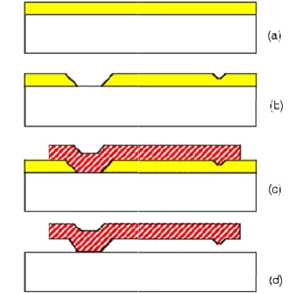
Fig. 1. (a) Sacrificial Layer deposition
(c) Metal Deposition and (d) Etch of sacrificial layer to free feature
In MEMS devices, such as the cantilever shown above, a sacrificial layer is deposited above the substrate. After patterned by photolithography and etching as shown in (b), a metal layer is grown over the layer. Wet etching can be used to remove the sacrificial layer. Now, the metal layer is affixed on one side but can flex on one side.
Dry Etch Methods
Dry Etching can be a physical or chemical process (or both)
• Ion Beam Etch - a physical etch process • Gaseous chemical etch
• Plasma enhanced etch • Reactive Ion Etch
Deep Reactive Ion Etch
Dry etching methods are largely replacing wet etch in nanofabrication. The advantages of dry etch processes include anisotropic etch profiles in some cases, and the possibility of high aspect ratios for features
Dry etching processes can include purely physical etching, chemical etching, or combinations of both. Each will be discussed separately.
Physical Dry Etch
In sputtering, air molecules are removed from the chamber and a low pressure inert gas, such as argon, is injected. RF plasma is created at low pressure, which creates an environment where the mean free path between the gas atoms is large. Normally, atoms would frequently collide, but in this environment, there are few remaining. The RF energy from the plasma acts on the Argon atoms.
h methods when the features below the photomask may be damaged by ion bombardment that occurs
(a) Sacrificial Layer deposition, (b) Patterning of layer, (d) Etch of sacrificial layer to free
feature
In MEMS devices, such as the cantilever shown above, a sacrificial layer is deposited above the substrate. After patterned by photolithography and etching as shown in (b), a metal layer is grown over the layer. Wet etching can be used to ficial layer. Now, the metal layer is affixed on one side but can flex on one side.
Dry Etching can be a physical or chemical process (or both)
a physical etch process
Dry etching methods are largely replacing wet etch in nanofabrication. The advantages of dry etch processes include anisotropic etch profiles in some cases, and the possibility of high aspect ratios for features on a device (depth .vs. width). Dry etching processes can include purely physical etching, chemical etching, or combinations of both. Each will be
[image:3.595.330.541.100.313.2]At the correct low pressure level, a single electron can impact an orbiting electron in an Argon atom, knocking it out of orbit. This creates an ion (positively charged) and a free electron that can be accelerated into another atom. A small percentage (much less than 1% typically) of the atoms is ionized. Some electrons are not knocked out of orbit by the electron that strikes the atom, but are excited to a higher energy level. As they drop back to the lower level, they give off the energy in the form of light, indicated by the characteristic plasma glow. The ion milling process is purely a physical process. It suffers from a lack of selectivity compared to other processes. It does provide an anisotropic etch profile with minimal undercutting.
Dry Chemical Etch
Certain gases, including chlorine and other halogens will react with the surface of a wafer to etch away material. The reactions are limited to the surface, and take place at a higher rate as temperature is increased. A flow of gas across the surface provides the reaction and removes the residues. A purely chemical dry etch reaction may be isotropic. The rate at which the etching occurs is limited by the surface, and it can be greatly increased by conducting the etch in the presence of plasma enhancement. Dry etch processes are capable of anisotropic etch profiles when enhanced by plasma, and are capable of smaller resolution. The dry etch process requires more sophisticated equipment including vacuum systems, RF sources for plasma generation, and much tighter controls on the process variables. Anisotropic etch profiles are profiles where the etching does not progress equally in all directions, and are often favored for tall feature creation
Remote Plasma Etch
Remote plasma (outside the reaction chamber) causes the gases to disassociate into ions and free radicals. The free radicals are highly reactive and pass into the chamber where they react with the surface to be etched. Although this increases the reaction rate, it does not improve the isotropic properties of the process. Plasma etch can be used for photoresist stripping in place of a wet etch process. Direct plasma etch with oxygen may also be used but concern for possible damage to the layer below from ion bombardment is required.
Reactive Ion Etch
Reactive Ion Etching combines both a physical and chemical etch process. Argon is used in a plasma as a physical etching process. The anisotropy of this process is retained, and the physical removal process causes the surface to continually be exposed to the chemical etching taking place from the radicals in the gas that have been formed from the plasma. The name reactive ion etching is something of a misnomer, as the ions in the etch are usually from an inert gas such as argon, and are not reactive. Ion assisted etching is a more accurate name for this process as the ion milling that occurs aids the chemical reaction. Reactive ion etching combines the anisotropic properties of the ion milling process with the increased speed of plasma enhanced chemical etching. The higher selectivity ratio of the chemical etch process is preserved in RIE, and small feature sizes can be defined. Reactive Ion Etching has become the process of choice in semiconductor processing, but
additional requirements for nanostructures and deep trench features in semiconductor processing for capacitors in DRAMs demand other processes. Plasma causes disassociation of chemical vapors into radicals that are highly reactive with the wafer surface. Plasma etching uses the inert gas to sputter or ion mill the wafer surface. Reactive ion etch uses the physical etch of the inert gas to remove surface molecules so that the chemical etch of the radicals from the dissassociated gas can perform their etch faster.
Deep Reactive Ion Etch
Tall features, such as comb-like structures found in RF-MEMS, filters, and other devices require processing techniques that will retain vertical sidewalls. The Bosch DRIE process accomplishes this by alternating etch steps with passivation coatings that are deposited on the sidewalls. The sidewall features may not be entirely flat, and may have a slight sawtooth structure, but undercutting is eliminated. In the cryrogenic process, both etch and passivation take place at the same time, but at temperatures near -110 degrees C. Smoother sidewalls and higher selectivity are advantages of this process, but more environmental control is required. By comparison, feature heights of well over 100uM can be realized with DRIE as opposed to 10uM or less with RIE.
RESULTS AND DISCUSSION
The emission of light occurs when electrons, ions or molecules in a high energy state relax to a lower energy state. In a plasma, gas molecules are broken into fragments and excited to high energy states by the applied radio frequency power. These fragments recombine giving off photons equal in energy to the difference between the excited state and the relaxed state called an emission spectrum. In general plasmas are quite complex and the emission spectrum has many spikes and peaks at different wavelengths. Some of these spikes and peaks change as the chemistry of the plasma changes. For example in etching silicon nitride once the etching is complete the amount of nitrogen in the plasma goes to zero and peaks associated with nitrogen disappear. If the nitride is over oxide than once the nitride is gone the amount of oxygen in the plasma will increase and peaks associated with oxygen will appear. Usually several signals are watched at the same time to determine end point in plasma etching.
Etch Rate: The etch rate during a plasma etch is determined
by system design, pressure and chemical species density. Because there is a direct correlation between power level and gas dissociation, higher power levels produce more ions and radicals. This in turn increases the rate of etch. The etch rate also can be influenced by the gas formula. Finally, the dry etch temperature influences the etch rate. Increasing temperature increases the etch rate. However, at temperatures exceeding 200ºC, the photoresist can bake, which will eventually render it difficult to remove from the wafer. Pressure levels also can influence the etch profile. If the pressure in the vacuum chamber is too high, particles begin to collide with each other and travel off in many directions. This results in an isotropic etch. In the pressure range of 0.4-50.0 mTorr, particle collisions can be kept to a minimum and anisotropic profiles can be achieved.
However, low pressure and high energy in the vacuum chamber can cause plasma radiation damage to the wafer. The resulting damage includes surface leakage, changes in electrical parameters, degradation of the film on the wafer and overexposure. It may also harden the photoresist, making it difficult to remove.
Micro-loading is a problem that can affect selectivity during the dry etch process. It occurs when the larger surface areas on the wafer etch at a slower rate than do smaller areas. As the larger areas etch, an abundance of by-product is produced. In turn, the amassed by-product slows down the etch rate. On the other hand, smaller areas are not affected by a buildup of by-product. Thus, the smaller areas etch faster than do the larger areas. In turn, the smaller areas are exposed to the chemical etchant for a longer period of time. This decreases selectivity in that region and promotes "ashing". Ashing occurs when the etch process removes the resist.
Post-etch corrosion: Another problem that can arise with dry
etch is post-etch corrosion. Post-etch corrosion occurs when residue from the etchant is left on the wafer surface after the final rinse. Often, this is a result of Chlorine (Cl) reacting with metals on the wafer surface. Using a fluorine-based gas mixture instead of a Chlorine-based gas mixture can eliminate this problem. In the present study, we discuss Properties, different methods and steps of etching for the semiconductor manufacturing process. There are number of advantage of plasma etching i.e No photoresist adhesion problems, Anisotropic etch profile is possible, Chemical consumption is small and Disposal of reaction products less costly.
REFERENCES
Chapman, Brian, Glow Discharge Processes, John Wiley and Sons, New York, 1980.
Elliot, D. 1996. Integrated Circuit Fabrication Technology, McGraw-Hill, New York, p.282
Lynn Fuller, 2013. Microelectronic Engineering, Rochester Institute of Technology, plasma etching.
Manos, D. and Flamm, D. eds., 1989. Plasma Etching, and Introduction, Academic Press, Inc., New York.
Maricopa Advanced Technology Education Center 2001. Module 47 “The Etch Process”
McGuire, Gary, E. 1988. Semiconductor Materials and Process Technology Handbook, Chap. 5. “Plasma Processing” and Chap. 6, “Physical Vapor Deposition”, Noyes Publications, Park Ridge, NJ.
Morgan, Russ, Plasma Etching in Semiconductor Fabrication, Elsevier Press, New York, 1985.
The Texas Engineering Extension Service, Semiconductor Processing Overview, Texas A&M University System, p. 139-153. 1996.
Van Zant, P. 1997. Microchip Fabrication, (3rd ed.). McGraw-Hill.
Van Zant, P. 2004. Microchip Fabrication (4th Edition) McGraw-Hill, New York.
Wolf, S. and Tauber, R. N. 1986. Silicon Processing for the VLSI Era, Vol 1, Chap. 10, “Physical Vapor Deposition”, and Chap. 16, “Dry Etching for VLSI”, Lattice Press, Sunset Beach, CA.
Xaio, Hong, 2001. Introduction to Semiconductor Manufacturing Technology Prentice-Hall, Upper Saddle River, NJ.