Partial Adiabatic Logic
Swathi S. Kendri
3rd sem Match
Department of Electronics &
Communication engineering,
K.L.E Dr. M.S. Sheshgiri College
of Engineering
& Technology, Belagavi
Rajashri Khanai,
PhD
Professor,
Department of Electronics &
Communication engineering,
K.L.E Dr. M.S. Sheshgiri College
of Engineering
& Technology, Belagavi
Swati Mavinkattimath
Assistant Professor
Department of Electronics &
Communication engineering,
K.L.E Dr. M.S. Sheshgiri College
of Engineering
& Technology, Belagavi
ABSTRACT
As the semiconductor industries is in progress which follows Gordon Moore‟s, Moore‟s law faithfully from the past five decades. Also, with integrating more number of transistors along with the functional circuits in a single chip with new process technologies [4]. Thus, with the increasing growth in VLSI technologies, per chip area the transistors number of counts is also constantly increasing, but with the same rate the chips gate switching energies does not decrease, thus the heat removal becomes more difficult with the power dissipation rise and even more costly [1]. The cost of that of total power consumption can be reduced with the advancement in the transistor process technology. As we know that power dissipation and a propagation delay are the fundamental building blocks in any digital hardware [6]. Hence limiting the power dissipation through adiabatic operation promises reduction of power consumption largely [1]. In VLSI, the adiabatic logic circuits are one of the promising low power techniques which gives low power dissipation with an expense of delay [6]. At first, the adiabatic logic circuits working principle are discussed. Next, the adiabatic switching and how it can conserve power is discussed. This report also tells about different types of adiabatic logic families and its classification as fully and partially adiabatic logics. This paper review also covers some of the important future research directions [1]. An emulative investigation is carried out on the proposed circuit in CADANCE tool at GPDK180nm technology node. Comparison has shown that it significantly saves power up to an extent of about a 70% of a proposed technique as compared to that of a conventional CMOS logic circuits within a transition frequency range of about 10 to 150MHz. The low power digital devices that is operated with a low frequency have strongly accepted the importance and the use of the emulation results obtained from this type of adiabatic logic circuits technique. Hence, a tiny circuit design, a high speed and an economical VLSI (Very Large Scale of Integration) circuits with low power dissipation of numerous circuits used today with this progress [4]. The present work proposes positive feedback adiabatic logics (PFAL) based Full-adder designs and is compared with the conventional CMOS circuit designs.
General Terms
Adiabatic Logic, Positive Feedback Adiabatic Logic (PFAL).
Keywords
Adiabatic logic, conventional CMOS logic circuit and PFAL logic circuit.
1.
INTRODUCTION
Many researcher‟s interest in the development of a technically acceptable low power VLSI design methodologies have demanded for an ultralow power system that are being
attracted as compared to a traditional strategy, which is been forecasted very recently [3]. With the present generation of devices are from the frequency of fundamental physical limits, for processing a new generation are being developed. Thus, needs for a VLSI chips with low power has raised from such evolution an integrated circuit were forced. In 1971, the Intel 4004 microprocessor was developed and had transistors count of 2300, that in turn about an 1watt of power dissipated with 1MHz frequency. After that a Pentium came in 2001, which had a 42 million number of transistors, which dissipated 65watts of power with 2.4GHz frequency. A few years later, the microprocessor designed also will have the same power as that of a nuclear reactor, if the power densities rise in an exponential way. Such high-power densities introduce the reliability concerns like thermal stress, electro migration and hot carriers induced a device degradation, which would result in the performance loss. Another factor is low power chips which in-turn needs fuel is of increased market demand in all the portable consumer electronics device which are powered through batteries. For the low power requirements, craving of the smaller with lighter and also the more durable electronic products is necessary. The electronics also dissipates more amount of heat with more power consumption, which in-turn requires more costly cooling solutions like for e.g. liquid cooling cabinets for desktop computers resulting to a higher overall cost of the device with IC. Thus, a product differentiator in almost all portable devices is the battery life. In the batteries life history, no such similar rapid solidity growth has occurred compared to that of electronic circuits even being the biggest and heaviest component in all the portable systems. The power dissipation is gaining prominence being main source in high performable portable digital batteries systems running on batteries like cellular phones, note-book computers and personal digital (PDA) assistants. These systems are directly related to the performance, which effects the battery longevity with a low power consumption as a prime concern [1].
A low power VLSI design has assumed greater importance for an active and rapidly developing field, in these situations. A greater number of transistors per chip with better performance in the development of the MOS technology is increasing, which is a main operating feature for any chip manufacturers [1]. Thus, in any integrated circuit (IC) the power consumption is one of a basic parameter. Always main parameters to meet the system requirement is the power and performance. Even on the system cost the power has a direct impact [2].
been recovered to the supplied power without any generation of heat using energy recovery principles in many adiabatic logic families has been proposed and implemented. Theoretically, by lagging the time of switching to a larger value it can be possible to reduce the dissipation of power [1]. Manufacturing to accommodate more integrating number of transistors per chip area in a single package of the chip and hence decreased not just the size but also has made it inexpensive with lesser delay [4].
2.
ADIABATIC LOGIC CIRCUITS
2.1. CMOS Logic Circuits Principal
In CMOS logic circuits, power dissipation is during the switching of devices primarily. The CMOS logic circuits consist of both PMOS and NMOS transistors with a switch, which is ideal and a resistor is connected in series to represent the effective channel resistance for the ideal switch and also with some of the resistance that are interconnected, as shown in Fig. 2.1.1. The load capacitance consists of two networks namely pull-up and pull-down network that are connected with a 𝐶𝐿 the node capacitance. There is a sudden flow of
current through the resistance R, when the systems logic level is “1” and the charge Q is written as
Q = 𝐶𝐿 . 𝑉𝑑𝑑 ----(1)
The power supply rail is positive and is charged from 𝐶𝐿 to
𝑉𝑑𝑑 with the charge supply as depicted in the equation 1.
Thus, at the power supply rail, the energy drawn is Q · 𝑉𝑑𝑑 = 𝐶𝐿 . 𝑉𝑑𝑑2
Now, let us assume that the node capacitance 𝐶𝐿 which is
equal to that of the drawn energy from the power supply, then in 𝐶𝐿 the total energy stored becomes one-half of the supplied
energy,
i.e.
𝐸
𝑠𝑡𝑜𝑟𝑒𝑑= 0.5.
𝐶
𝐿. 𝑉
𝑑𝑑2Thus, through the resistance R, the energy remaining gets dissipated.
Similarly, during the discharging, in NMOS pulldown network, the same amount of energy is dissipated when the systems logic level is “0”. Thus, during the charging and discharging the total amount of the dissipated energies as heat is
𝐸
𝑡𝑜𝑡𝑎𝑙=
𝐸
𝑐ℎ𝑎𝑟𝑔𝑒+
𝐸
𝑑𝑖𝑠𝑐 ℎ𝑎𝑟𝑔𝑒----(2)
= 0.5
. 𝐶
𝐿.
𝑉
𝑑𝑑2+ 0.5
. 𝐶
𝐿.
𝑉
𝑑𝑑2=
𝐶
𝐿. 𝑉
𝑑𝑑2It can be concluded that the consumption of energy in a conventional CMOS logic circuit is reduced through the reduction in the 𝑉𝑑𝑑 from the equation 2. Thus, the power consumption (i.e. P = dE/dt) also can be reduced proportionally with the decreasing of the switching activities of the circuit [1].
2.2. Adiabatic Logic Circuits Principal
A familiarly used technique for minimizing the energy losses during charging and discharging is adiabatic logic switching. The word “adiabatic” is derived from a Greek word called adiabatos and it means impassable. Adiabatos are without heat loss or gain, a change of state occurs [1]. The thermodynamic in which no energy transfers through the environment, and hence the word “Adiabatic” is been taken from and even there is no dissipated energy losses [5]. The ideal process in acircuit cannot be achieved because the dissipative elements are present such as resistance in reality computation. Under the certain conditions by only switching the transistor and by slowing down speed of operation the energy dissipation reduction can be achieved. Adiabatic logic circuits consider the „reversible logic‟ to conserve energy and hence are considered as a low power circuit. In order to reduce the dissipation of power, at a constant current all nodes are charged or discharged during the adiabatic switching. With the help of an AC power supplies to charge the circuits at the starting stages during the particular adiabatic phases and then discharges the circuit for recovering with the supplied charges can be accomplished. With the conventional switching technique of dissipation, the principles of adiabatic switching can be explained better. The energy gets dissipated during the switching transitions of an adiabatic logic circuits with respect to a varying input is as shown in the Fig 2.2.1[1].
Fig. 2.1.1: A Conventional CMOS model along with charging and discharging
Fig 2.2.1: An Adiabatic logic model along with charging and discharging
The switching transitions rate decreases in the adiabatic circuits, in contrast with the conventional charging, instead of using a fixed voltage supply sources but the use of a voltage source with time-varying. With time the changes in each voltage, as shown in Fig. 2.2.2. By fortifying a systematic charge transfers over a total available time, the peak current can be reduced of the adiabatic circuits. Hence through 𝐶𝐿 is
the average current Iˆ is flowing, then during the transition phases the overall energy dissipation can be reduced proportionally as follows: [1]
Theoretically, when driving voltage‟s φ, time changes from 0V to 𝑉𝑑𝑑 during the adiabatic charging the 𝑇𝑝 becomes long
and power dissipation is nearly zero. The discharging in the pull-down network through the NMOS transistor occurs, when φ changes from 𝑉𝑑𝑑 to 0V. Hence, the dissipated power
is reduced with the decrease in the switching transitions rate from the equation 2, during a given computation steps the capacitors draws some energy in the system that is stored and uses it in subsequent computations. The signal energies instead of being dissipated as heat can be recycled. With the theory of charge recovery principles, the systems must be noted that above mentioned are not necessary to be reversible [1].
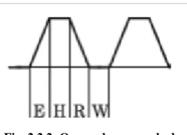
quarter of period of phase difference is considered in the adiabatic operation. Wait, Evaluate, Hold and Recovery are the four operation phases respectively which is as shown in the Fig. 2.2.2. By maintaining the output with the low value, the clock power stays low(zero) value in the WAIT phase. A pre-valuated result is generated with the evaluation logic. The pre-valuated inputs will not be affected to the state of a gate, since the power clock is low level at present. As per the pre-valuation logic the outputs will be valuated with the power supply being ramped from zero to 𝑉𝑑𝑑 gradually in
[image:3.595.325.535.75.190.2]EVALUATE phase. For the pipelining of next stage in adiabatic circuits with the clock power keeping high by providing a unchangeable input signal and keeping the outputs valid until the entire phase of the HOLD phase. The inputs are being ramped down to low value, in the meanwhile. The energy instead of being dissipated as heat, at the circuit node energy can be recuperated back to the power source with the power supply being ramped down to zero, in the RECOVERY phase [8].
Fig. 2.2.2: One cycle power clock
In Adiabatic Switching the primary part in the whole adiabatic logic system design is a power clock generator. The power clock used here constitute of a frequency and voltage levels and hence is a mixture of power supply and clock.
2.3. A Simple Adiabatic Logic Gate
[image:3.595.330.529.220.346.2]To examine, let us consider a simple circuit with the adiabatic switching configuration. A general circuit of the conventional CMOS logic gates and the adiabatic correlative is as shown in the Figure 2.3.1. A pull-up transistors and pull-down transistors network can be replaced with a complementary T-gate or also called as a transmission-T-gates, in order to transfigure the conventional CMOS logic gate through an adiabatic logic gate. To drive the output of the adiabatic gate, the T-gate networks for implementing the pull-up functions is used, while to drive the complementary output node, the T-gate networks for implementing the pull-down functions is used [1]. Also, the inputs should be available in the complementary forms. Both pull-up and pull-down networks of the adiabatic logic circuits are used for charging/discharging the consequence node capacitance, which tells that the stored energy at the consequence nodes can be recaptured by the power supply, at the end of each cycle as shown in the Figure 2.3.2. In the adiabatic operation, the voltage source of the conventional CMOS circuits being DC should be replaced with a varying supply of power with that of a ramped voltage consequence [1].
Figure 2.3.1: A Simple Adiabatic Logic Gate
Fig. 2.3.2: An Adiabatic Logic Gate showing Charging and discharging path
An adiabatic logic circuits device count with the necessary circuit alterations which are used for the conversion of a conventional CMOS logic circuit is increased by a factor of two or even sometimes even more [1].
3.
ADIABATIC LOGIC FAMILIES
Adiabatic logic circuits classified into two types [1]: (a) Quasi/ Partial Adiabatic Logic Circuits
(b) Full Adiabatic Logic Circuits
3.1. Quasi/Partial Adiabatic Logic Circuits:
Quasi/partial adiabatic logic circuits have a straight forward architecture with power clock system. The adiabatic losses do exits, and occurs in non-ideal switches during the current flows through them, that are proportional to that of the power-clocks frequency. Some of the well accepted Partially Adiabatic families are namely [1]:(i) Efficient Charge Recovery Logic (ECRL). (ii) Positive Feedback Adiabatic Logic (PFAL). (iii) 2N2P Adiabatic Logic(2N2PAL)
(iv) 2N Adiabatic Logic(2NAL).
(v) Source-coupled Adiabatic Logic (SCAL). (vi) Clocked Adiabatic Logic (CAL). (vii) NMOS Energy Recovery Logic (NERL). (viii) True Single-Phase Adiabatic Logic (TSEL).
3.2. Full Adiabatic Logic Circuits:
[image:3.595.101.236.279.376.2]face a lot of problem with the speed of operations and also with power clock synchronization of the inputs. Some of the Fully adiabatic logic families are namely [1]:
(i) Pass Transistor Adiabatic Logic (PAL).
(ii) Two phase adiabatic static CMOS logic (2PASCL). (iii) Split- Rail Charge Recovery Logic (SCRL).
4.
POSITIVE FEEDBACK ADIABATIC
LOGIC(PFAL):
[image:4.595.317.541.72.285.2]A Positive Feedback Adiabatic Logic (PFAL) is being used here is a partial/quasi adiabatic logics family. It is considered as a partially energy recovery circuit since it consumes a very low energy when compared to that of other familiar families. Also, it has a good durability against the technological parameter variations. It consists of partial energy recovery with dual-rails circuit. The general schematic diagram of the PFAL circuits is as shown in the Fig. 4.2[1].
Fig. 4.2: The general schematic of the PFAL gate.
The PFALs core is an adiabatic amplifier, that is a latch with the two PMOSFET‟s M1 and M2, and of the two NMOSFET‟s M3 and M4, due to which the logic level degradation at the output nodes out and /out can be avoided. It also consists of two n-trees which is used to realize the logic functions. This type of partial adiabatic logic families generates a positive output and also the negative outputs too i.e. the compliment of the positive. All the functional circuits blocks are connected in parallel with that of PMOSFET‟s of the adiabatic amplifier and a transmission gates and is thus formed.
The two major differences between the ECRL are that the latch is made with the two P-channel MOSFET‟s and also two N-channel MOSFET‟s in PFAL, instead of considering only the two P-channel MOSFET‟s in case of ECRL logic, and the transmission gates of P-channel MOSFET‟s that are in parallel with the functional circuits blocks. Thus, the resistance equivalently gets reduced during the charging of capacitance.
5.
IMPLEMENTATION
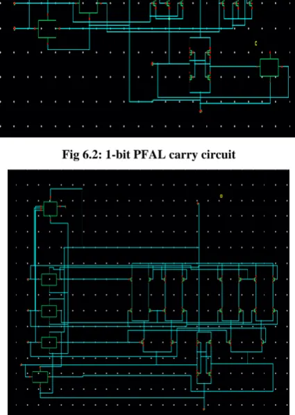
[image:4.595.60.269.280.409.2]Here in this seminar I have implemented a 1-bit full adder in cadence tool using gdpk180nm of both a conventional CMOS logic circuits, shown in Fig. 6.1 and using positive feedback adiabatic logic which is partial adiabatic logic type, as shown in Fig.6.2 and Fig 6.3.
[image:4.595.319.538.320.535.2]Fig. 6.1: 1-bit full adder using conventional CMOS circuit
Fig 6.2: 1-bit PFAL carry circuit
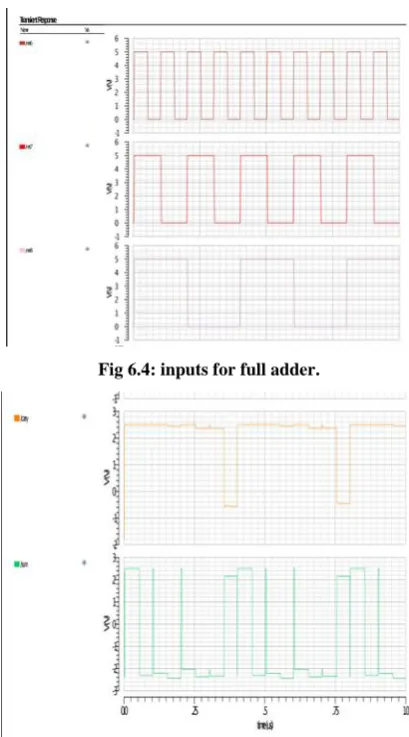
[image:4.595.321.534.371.670.2]Fig 6.4: inputs for full adder.
Fig 6.5: output waveform of conventional CMOS circuit
[image:5.595.316.540.94.294.2]A waveform for full adder is also observed. Here Fig 6.4. shows the inputs for the full adder. The output of conventional CMOS logic circuit is shown in Fig 6.5 and similarly the output of the PFAL logic circuit is shown in Fig 6.6.
Fig 6.6: output waveform of PFAL logic circuit
Further, the difference of both conventional CMOS logic circuit and PFAL adiabatic logic circuit for a 1-bit Full adder is tabulated in the below table Table 6.1.
Table 6.1. Comparison of conventional CMOS circuit and PFAL logic circuit
Parameters
Conventional CMOS logic
circuit
Positive feedback
adiabatic logic
(PFAL)
Number of
transistors 28 transistors
24 transistors (carry) + 32 transistor (sum) = 56
Area
consumption Less More
Power dissipation (𝜇m) [7]
1.9 0.05
Complexity Less More
Power supply DC power
supply Variable AC power supply
6.
CONCLUSION
The above study shows that the partial/quasi adiabatic logic circuit is a technique for the reduction of the energy dissipation, when compared to that with a conventional CMOS logic circuits switching under certain circumstances. All the input signals must be a controlled transition in the form of a ramp in adiabatic circuits, when compared with that of a conventional logic switching where only the input signals which have the different final logics state changes. The energy dissipation can be reduced by not switching instantaneous instead must be gradual process. In this paper, as we have examined with the circuits a low energy dissipation can be achieved with no significant improvements in rise/fall times. Due to the finite state of the threshold voltage of a MOS transistors these limitations are achieved and possibly to even a lesser extent of nonlinearity characteristics of the MOSFETs channel resistance.
It has been also observed that in the fully adiabatic logic circuits the power consumption can be significantly reduced but have a very complex design when compared to that of partially adiabatic circuits, which are not as efficient as fully adiabatic circuits, in terms of a power consumptions, but can reduce the circuit complexity and simultaneously conserve power too. So, we can say that the quasi/partially adiabatic logic circuits are fair compromise in the complexity trade-offs and the power consumptions.
7.
FUTURE WORK
[image:5.595.62.268.506.700.2]8.
ACKNOWLEDGMENTS
I sincerely express my deep sense of gratitude towards my respected guide Dr. Rajashri Khanai and co-guide Mrs. Swati Mavinkattimath for their valuable guidance, profound advice, persistent encouragement and help during the completion of this work. Their time to time helpful suggestions boosted me to complete this task successfully.
9.
REFERENCES
[1] Deepti Shinghal, Amit Saxena, Arti Noor, “Adiabatic Logic Circuits: A Retrospect”, MIT International Journal of Electronics and Communication Engineering, Vol. 3, No. 2, August 2013, pp. 108–114, ISSN No. 2230-7672 ©MIT Publications.
[2] Benjamin Gojman. “Adiabatic Logic”, August 8, 2004. [3] Atul Kumar Maurya, Gagnesh Kumar, “Adiabatic Logic:
Energy Efficient Technique for VLSI Applications”, International Conference on Computer & Communication Technology (ICCCT)-2011, 978-1-4577-1386-611.
[4] Tabassum Ara, Amrita Khera, “Performance Evaluation in Adiabatic Logic Circuits for Low Power VLSI Design”, International Journal of Engineering Trends and Technology (IJETT) – Volume 45 Number 5- March 2017, ISSN: 2231-5381, http://www.ijettjournal.org.
[5] Preeti Bhati, Navaid Z. Rizvi, “Adiabatic Logic: An Alternative Approach To Low Power Application Circuits”, International Conference on Electrical, Electronics, and Optimization Techniques (ICEEOT) – 2016, 978-1-4673-9939-5/16.
[6] H.V. Ravish Aradhya, H R Madan, M S Suraj, “Design and Performance Comparison of Adiabatic 8-bit multipliers”, 978-1-5090-1623-5/16.
[7] Keval Kamdar, Aishwarya Acharya, Poonam Kadam, “Low Power Multiplier Design using Adiabatic SCRL Logic”, Proceedings of 2017 IEEE International Conference on Circuits and Systems (ICCS2017), 978-1-5090-6480-9/17.
[8] Akash Agrawal, Tarun Kumar Gupta, Ajay Kumar Dadoria, “Ultra Low Power Adiabatic Logic Using Diode Connected DC Biased PFAL Logic”, theoretical and applied electrical engineering, volume 15 , number 1, march 2017, advances in electrical and electronic engineering.
[9] Y. Sunil Gavaskar Reddy and V. V. G. S. Rajendra Prasad, “Power Comparison Of Cmos And Adiabatic