CADLINC INC.
Processor Specifications
Nu.ber:
Author:
Approved:
000014 Rev: A
~
.. /.
a
/~.~.~
~--- ---~~
Georse A. iewicz
p-~--~
TABLE
or
CONTENTS1. Introduction •••••••••••••••••••••••••••••••••••••••••••••••••••• 1
2. Overview of Operation ••••••••••••••••••••••••••••••••••••••••••• 2
2.1. Central Processins Unit (CPU) ••••••••••••••••••••••••••••••••• 2
2.2. "eaorw.I •••••• ~ •••••••••••••••••••••••••••••••••••••••• ••••••• 2
2.3. Busei ••••••••••••••••••••••••••••••••••••••••••••••••••••••••• 2
2.4. InPUt - OutPut Devices •••••••••••••••••••••••••••••••••••••••• 3
2.5. InterrUPts •••••••••••••••••••••••••••••••••••••••••••••••••••• 3 2.6. Boot State •••••••••••••••••••••••••••••••••••••••••••••••••••• 3
2.7. He.orv Hanase.ent ••••••••••••••••••••••••••••••••••••••••••••• 4
3. Theorv Of OPeration ••••••••••••••••••••••••••••••••••••••••••••• 5
3.1. Introduction •••••••••••••••••••••••••••••••••••••••••••••••••• 5
3.2. Control Losic ••••••••••••••••••••••••••••••••••••••••••••••••• 5
3.2.1. Co •• and Generation ••••••••••••••••••••••••••••••••••••••••• 16
3.2.1.1. Status Co .. ands •••••••••••••••••••••••••••••••••••••••••• 19
3.2.1.2. Svste. Access Co •• ands ••••••••••••••••••••••••••••••••••• 20
3.2.1.3. Hanased Access CO •• ands •••••••••••••••••••••••••••••••••• 21
3.2.2. Reset Lo.ic •••••••••••••••••••••••••••••••••••••••••••••••• 22
3.2.3. Boot Lo.ic ••••••••••••••••••••••••••••••••••••••••••••••••• 23
3.2.4. Interrupt Losic •••••••••••••••••••••••••••••••••••••••••••• 25 3.3. Heaorv H.na!e.ent •••••••••••••••••••••••••••••••••••••••••••• 27 3.3.1. Svste. Accesses •••••••••••••••••••••••••••••••••••••••••••• 27
3.3.1.1. Heaorv "a~ ••••••••••••••••••••••••••••••••••••••••••••••• 28
3.3.1.2. Context R •• ister ••••••••••••••••••••••••••••••••••••••••• 30
3.3.1.3. Proas •••••••••••••••••••••••••••••••••••••••••••••••••••• 32
[image:3.613.92.502.125.758.2]3.3.1.4.1 •. Introduction ••••••••••••••••••••••••••••••••••••••••••• 33
3.3.1.4.2. Functional Descri~tion ••••••••••••••••••••••••••••••••• 34
3.3.1.4.3. Ti.er Co •• ands ••••••••••••••••••••••••••••••••••••••••• 3S
3.3.1.4.4. Cadlinc OPeratint Hodes •••••••••••••••••••••••••••••••• 36
3.3.1.5. Intel 8274 UART •••••••••••••••••••••••••••••••••••••••••• 38
3.3.1.5.1. Introduction ••••••••••••••••••••••••••••••••••••••••••• 38
3.3.1.5.2. Functional Description ••••••••••••••••••••••••••••••••• 38
3.3.1.5.3. UART Co •• ands •••• '.. • •••••• • •••••• •• • • • • • • • • •••• • • •• •••• 39
3.3.1.5.4. Cadlinc Operatins Hodes •••••••••••••••••••••••••••••••• 39
3.3.1.6. Parallel InPUt Port •••••••••••••••••••••••••••••••••••••• 41
3.3.1.7. Hardware VPA ••••••••••••••••••••••••••••••••••••••••••••• 41
3.3.2. Hanased Accesses ••••••••••••••••••••••••••••••••••••••••••• 42
3.3.2.1. Raa He.orv ••••••••••••••••••••••••••••••••••••••••••••••• 42
3.3.2.1.1. Locll He.orv ••••••••••••••••••••••••••••••••••••••••••• 43
3.3.2.1.2. Local Parity Lotic ••••••••••••••••••••••••••••••••••••• 44
3.3.2.1.3. HiShspeed Bus Interface •••••••••••••••••••••••••••••••• 46
3.3.2.2. Hultibus Interface ••••••••••••••••••••••••••••••••••••••• 47
3.3.2.2.1. Bus Haster Arbitration ••••••••• • i. I f • • • • • • • • • • • • • • • • • • • • 47
3.3.2.2.2. He.orv Access •••••••••••••••••••••••••••••••••••••••••• 48
3.3.2.2.3.
r-o
Access ••••••••••••••••••••••••••••••••••••••••••••• 484. Bo.rd Kne.onies •••••••••••••••••••••••••••••••••••••••••••••••• 49 4 .1. Buses'. • • • • • • • • • • • • • • • • • • • • • • • • • • • • • • • • • • • • • • • • • • • • • • • • • • • • • •• S2 4.2. Ca..lnds ••••••••••••••••••••••••••••••••••••••••••••••••••••• 53
4.3. Co •• unic.tians ••••••••••••••••••••••••••••••••••••••••••••••• S9
4.4. Hishspeed Bus •••••••••••••••••••••••••••••••••••••••••••••••• 61
4.5. Hultibus ••••••••••••••••••••••••••••••••••••••••••••••••••••• 63
4.7. Heaorv Hanase.ent •••••••••••••••••••••••••••••••••••••••••••• 67
Appendix A - Ju.per Options ••••••••••••••••••••••••••••••••••••••••• 69
Appendix A.l J81 •••••••••••••••••••••••••••••••••••••••••••••••••• 69
Appendix A.2 JB2 •••••••••••••••••••••••••••••••••••••••••••••••••• 70
Appendix A.l J8l •••••••••••••••••••••••••••••••••••••••••••••••••• 71
Appendix A.4 JB4 •••••••••••••••••••••••••••••••••••••••••••••••••• 72
Appendix B Initial He.orv Happins ••••••••••••••••••••••••••••••••• 73
Appendix C - Hultibus Bus Pin Assisnaents (Pl) •••••••••••••••••••••• 79
Appendix D -·Hishspeed Bus Pin Assisn.ents (P2) ••••••••••••••••••••• 80
Appendix E Co •• unications and Parallel Ports •••••••••••••••••••••• 81
Appendix F Protection PRO" Code ••••••••••••••••••••••••••••••••••• 82
Appendix G PAL Codes •••••••••••••••••••••••••••••••••••••••••••••• 84
Appendix G.l PALPO •••••••••••••••••••••••••••••••••••••••••••••••• 85
Appendix G.2 PALP1 ••••••••••••••••••••••••• · ••••••••••••••••••••••• 86
Appendix G.l PALP2 •••••••••••••••••••••••••••••••••••••••••••••••• 87
Appendix G.4 PAlPJ ••••••••••••••••••••••••••••••••••••••• i •••••••• 88
LIST OF TABLES
Table 1 - S~5te. Access State Flow •••••••••••••••••••••••••••••••••
a
Table 2 Hana~ed Access State Flow tor Hishspeed Access ••••••••••• 11
Table 3 - Hanased Access State Flow tor Multibus Access •••••••••••• 14
Table 4 - He.or~ Hana~e.ent Address Translation •••••••••••••••••••• 28
Table 5 - Pa~e Hap Data Entries •••••••••••••••••••••••••••••••••••• 29 Tlble 6 Context Re~ister Data For.at ••••••••••••••••••••••••••••• 30
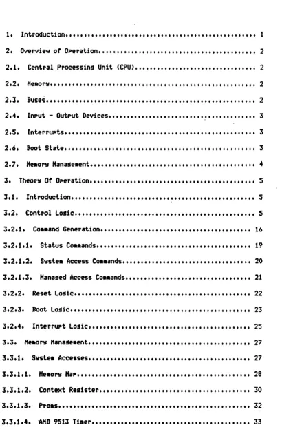
[image:6.623.91.506.95.773.2]Fi.ure 1
Fi§ure 2
Ft.ur. 3
Fi.ure 4
Fisur. 5
Fifure 6
FilUre 7
Fi.ure 8
LIST OF ILLUSTRATIONS
Control Lo.ic Block Di •• r •••••••••••••••••••••••••••••••• 6
Svste. SPice Access Ti.in •••••••••••••••••••••••••••••••• 7
Ra •• nd Hilhspeed Access Tl.in •••••••••••••••••••••••••• 10
Hultlbus Access Ti.in ••••••••••••••••••••••••••••••••••• 13
Clock State Generator Circuit ••••••••••••••••••••••••••• 17
CO •• and Generation •••••••••••••••••••••••••••••••••••••• 18
Reset Circuit ••••••••••••••••••••••••••••••••••••••••••• 24
Boot Circuit •••••••••••••••••••••••••••••••••••••••••••• 24
Fi.ure 9 Interrupt Control Circuit ••••••••••••••••••••••••••••••• 26
Fifure 10 Ti •• r Function Di •• r ••••••••••••••••••••••••••••••••••• 37
Fifure 11 UART Function Dia.r •••••••••••••••••••••••••••••••••••• 40
1. Introduction
The CADLINC Series BOA Processor board consists of a Motorola 68000 central processins unit. RAM and PROM .e.or~, so.e 1/0 facili-ties, a local HIGHSPEED .e.or~ bus and an IEEE-796 MULTIDUS
*
inter-taee. Onboard .e.or~ consists of 4 JEDEC st~le b~te-wide PROM sock-ets, and 2S6K b~tes of d~na.ic RAM. The 1/0 facilities are two serial co •• unications ports, a 16-bit bidirectional port and a S channel
pro-sra •• able ti.er.
The Series BOA Processor can be used as a standalone s~ste. with onl~ a power suppl~, backplane and serial ter.inal, or as part of a fully inte~rated co.puter syste. that can include the CADLINC GRAPHICS CONTROllER, ETHERNET board, MULTIFUNCTION board, DUAL PORT MEMORY boards, FLOATING POINT Processor board, INTELLIGENT SERIAL CONTROLLER board and .an~ other HULTIBUS cOIP3tible peripherals.
2. Overview of Operation
2.1. Central Processins Unit (CPU)
The Kotorola 68000 has a 16-bit data bus and a 23-bit address bus. The internal resisters are 32-bits in lensth. It has 8 data and 7 address resisters. 2 stack pointers. a proSra. counter. plus a 16-bit status word. Operations on data .ay be byte (8), word (16), or Ions word (32 bits). Operations on addresses _ay be ot word or Ions word lensth. All resisters .ay be used as indexes. The 68000 has 2 states of operation: Supervisor and User for enhanced syste. inteSritv
and security.
Onboard PROH consists ot 4 JEDEC stvle PROH sockets that can accept 2732, 2764, 27128 or 27256 type ROHs (total capacity of 16K, 32K, 64K or 128K bytes respectively).
Onboard RAH cOllsists of 36 64K x 1 dYna.ic ra.s dvins a capacity of 256K bytes with paritv. RAH refreshinS is done by a PROH .onitor routine that executes 128 NOP instructions every 2 .illiseconds. The prosra •• able ti.er sene rates the Non-Haskable- Interrupt.
2.3. Buses
The CADLINC Series aOA Processor has 3 bus structures. The first is the internal svnchronous bus for Svste. accessed 1/0 and Heaerv Hanase.ent; the second is a proprietarY synchronous HIGHSPEED BUS on the Auxiliary HULTIBUS connector for expanded DUAL PORT HEHORY, FLOAT-ING POINT and ENHANCED SERIAL Processor boards; and the third is the HUlTIBUS for expanded off-the-shelf peripherals. i.e. Disc controll-ers, ETHERNET, GRAPHICS CONTROllER, etc. Svste. I/O devicu and onboard RAH do not reauire the use of the HUlTIBUS.
1. Onboard ae.orv accesses are faster than the Hultibus.
2. The HULTIBUS is then available for use by other bus .asters without havins to contend for priority very often.
3. DUAL PORT HEMORY responds IS fast as onboard RAH and is i •• ediately available to other bus .asters.
2.4. Input - Output Devices
The Series BOA Processor board has a dual channel UART chip, S prosraaaable ti.ers, and a 16-bit bidirectional port tor seneral pur-pose use. One of the UART's channels is contisured to coaaunicate with a terainal or CADLINC keyboard dependins on the PROH aonitor sup-plied. The other channel can be Juapered with another coaputer or a
second terainal. The line drivers and receivers are RS-423 coapatible and the connector pinouts are RS-232-C confisuration. Two at the tive
16~bit counter/tiaers are dedicated baud-rate Senerators for the U~RT chip, one tiaer channel tor each serial channel. One tiaer is dedi-cated to Sene rate a 2-aillisecond interrupt to retresh dYnaaic RAH. One of the two reaainins tiaers is aVlilable for user IPplications. The other acts as a ·Watchdos· tiaer to auto.aticallY reset the systea if the PROM .onitar proSra. has lost control. The 16-bit bidirec-tional port is desisned tor readins options selections froa a bank of
switches and to write status intoraation to a static displaY. .
2.5. Interrupts
The 68000 has seven interrupt levels and I current interruPt
level .ask. An interrupt will be processed if its level is Sreater than the current aask. Level 7, the hishest priority. is Non-Haskable and will alwavs interrupt any task. This level is reserved for the dyna.ic RAH refresh routine.
The standard HULTIBUS confisuration detines interrupt levels INTO to INT7, with INTO beins the hishest priority. The CADLINC Series BOA Processor defines priorities accord!ns to the Hotorola conventions with INT1 as the hiShest. INTO, then, is not iapleaented and INTI is the lowest prioritv.
PreassiSned interrupts on the.CADLINC Series ~ Processor are IS
tallows:
INT7: INT6: INTS:
Refresh tiaer (Non-Haskable) User prosra.aable ti.er UART sene rated interrupts
Interrupts are processed by the 68000 in 'Auto-Vector' aode only. Transter vectors are supplied troa an internal table, so the inter-ruptins device need not supply a vector.
2.6. Boot State
Boot State is terainated b~ one write to the S~stea Access loca-tion CLEARBOOT. See Device addresses.
The Heeorv Hanaieaent s~stea has been desi~ned to support a aulti-taskins operatini svstea. The concept, in short, is that ot
translatins, or aappins, Processor address bits A12-A21 (or A22) into ph~sical address bits HA12-HA23, alons with Protection, Address Space Allocation and Pase Control inforaation about each Pa~e.
All accesses to local RAH and to HULTIBUS aeaorv Ind I/O are translated and protected in the saae aanner.
Hanased Address access is initiated bv Processor address bit A23. When it is ·on·, Heaorv Hanaseaent is disabled and indicates a Svste. Access is to be perforaed. When it is ·off·, then the Processor addresses A12-A21 (or A22) co.bine with pre-pro~raaaed Context bits to for. a pointer into a 4K x 20 bit Arrav. The output of this Arrav con-tains the 12-bit Happed ph~sical address and B Protection arid alloca-tion bits. The 12 HanaSed Addresses co.aine with the lower 11 Proces-sor addresses to fora the 23-bit ph~sical address, ~ivins • full 16M
b~tes of phvsical space.
There are two aodes of coabinini Context bits with Processor addresses: One· with 1 Context bit, hence 2 levels of Context; the other with 2 Context bits havins 4 levels of Context. In the first aode, Cont~xt bit CXO co.bines with Processor address bits A22 and A21 as the .ost sisnificant bits into the Arrav. 'In the second, Context bits CX1, CXO and Processor address A21 are the aost sisnificant. Hence, the first aode ~ields 2 Contexts of 8H bvtes .ach and the second ~ields 4 Contexts of 4H bvtes each.
Context bits CXO and CXI are accessabl. vi. I Svste. Access
loca-tion. See Device Addresses.
3. Theor~ Of Operation
3.1. Introduction
The Processor divides UP its 16 Hb~tes of address space into two
8 Hb~te resions: S~ste. Space and Hanased Space. Systea space
coaprises the on-board PROHs, Tiaer, Uart, Parallel Port and Heaor~ Hanase.ent resisters. Hana~ed space consists at Local Heaor~, the Hishspeed bus and Hultibus accesses.
Hanased space is divided into 2 (or 4) Contexts, each capable of containins processes as lar~e as 8 Hb~tes (or 4 Hb~tes) in ph~sical aeao~. The Heaor~ Hanase.ent Unit contains 4096 entries that filter Virtual Processor addresses into Ph~sical addresse~ and supports the full 16 Hb~tes of ph~sical space.
3.2. Control Losic
See scheaatic drawinss tSD29S014
See Appendices F and G for tir.ware codes. See Fisure 1 Control Block Diasraa
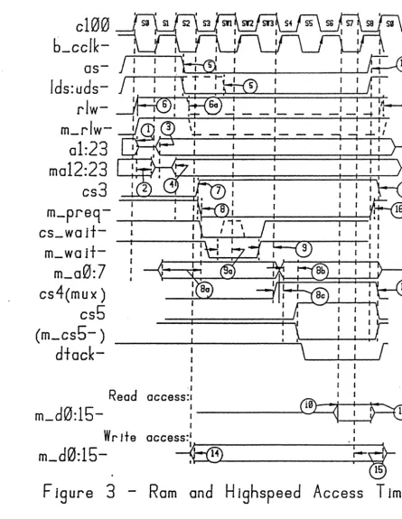
The Series BOA Processor board aakes exten~ive use of Prosraa.-able Arra~ Losic I.C.s to perfor. necessar~ co.aand ti.ins and direc-tion control. Fisure 1 is an overall block diasra. that shows the flow of input control and output co •• and sisnals.
The followins State Tables and Ti.ins Diasraas describe in Sen-eral the actions of the control losic. Reter to the PAL eQuations in Appendix G.
FIgure 1 - CadI Inc
r -
-
-
-
-
-
-
-
-
.- -,
Ser Jes
80A
I
H
Ighspeed
I
r - - - i
Data and
I
I
J2
Connector
I
Address
I
r -
-
-_. -
-
-
-1Jl
Connector
I
Buffers
I
Processor
I
I
Local
P2
I
I
I
256k
byte
i
I
Decode
S 10
TIMER·
I
I
L - , 023- d8-
I
I
. . - - - . , 019
dIS
-
-
-
-
-
.JL..
Data
-,
Commands
I
---,
Address
68000
CPU
r - - - -
"1I
7
InterruptI
I
I
LInes LogIcI
t
I
PI
I
Command
Generat Jon
I
I
I
I
-,---,..---r---r---r--..=!.. .-1
Memory
Management
L _ _ _ _ _ _ -'
I I
I
SID
IL..---'
Tlmer---'
I
RefreshI
Hult Ibus
Data
Buffers
Hultlbus
Address
Latches
HuH Jbus
Commands
\.
\
I
!
I
I
I
I
I
I
I
I
I
L _ _ _ _ _ _ _ .J
[image:13.803.34.749.62.581.2]1 , 1 1 1 1 1 I
clee
i:
5e
~:
51
V:
52
~
53
I
54 \
55
I
56 \
57
I
58 \
59
I
51e \ 511
I
512
~
513
r
01:
23
kft7l
;~
;
>
0.-:
Q)'
0
I\~
1 ),
I I~ , I I
r -
Ii
'
.
I, rI
w-~ ~ : \. _ _60 ________________________________________
~_
~_ ../
( Jds-
:\~---\,
~
uds-) I
~I
~
cs3
:!t--0
:
L .
I I I
sysacc- I
,
xae:ll
<
~----~---~~:A-- (en.mapx-we.mapx- )
____________________ ~ ________________________ ~ I I I
~~I---_r_4V
:
I ,
(devenab-ce.dev Jees-
'\~-~i---~~'.~---_r---~---~: ~
I , ,ce.map- ) cs6 (
Jorc-lowc- ) csle
diac~-WrJie de:15 Read de:15
I I I
I
AI
I~l
I /1 : I I
________________________
~---~-J I---~---;I ~
~---N~,--..--..---, ---..--~~{ ~
A
1\'- ...
- - - + - - - / :
Iffi7
I· \-~LW-J
II
:,~,
14~
_______________________
' ____
~~~:~I:
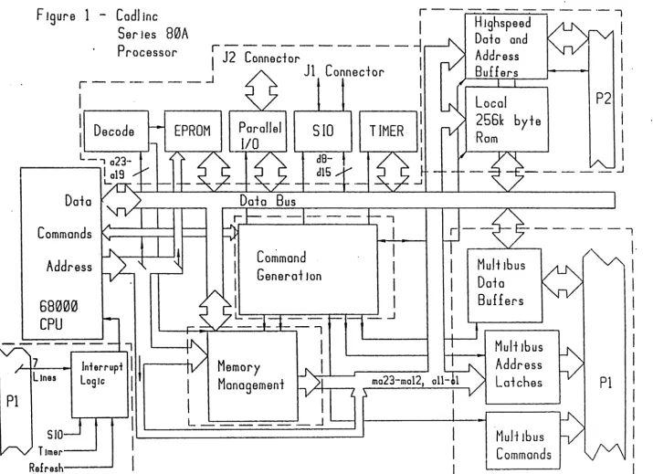
I State I Description (See Figure 2) I
1 __________ --1 ________________________________________________________ 1
f State
o.
1 Processor addresses a1 thru a23 are negated ('1). I 1 1 r/w- is asserted to a Read ('6) at the end ot everY I1 1 c~cle. I
1 I 1
1 ____________ 1-- __________________________________________________ 1
I State 1. I Processor addreses a1 thru a23 are asserted ('3). I I I a23 is high indicatins a Systea access reauest. SyS- I
f I tea device address decodes. 1
1--_____ ---__
1_--___ ---_---_---1
State 2. 1 Processor strobes ('S- for all ~cles, lds:uds- tor I I read c~cles) becoae valid ('5). sysacc is asserted I I ·hiSh·. ds senerated in a Read c~cle. For a Write 1I c~cle, r/w- is asserted (.6a). 1
1 I
____________ 1 _____________________________ _ .. ____ --1
State 3. 1 cs3 asserted ('7). Processor drives Data Bus dO:d15 I
I for a Write c~cle (U-U. 1
____________ 1 _____________________________________________________ --1 State~. I cs~ ('7) asserted. Hultiplexed Addresses now switch I I to upper Processor addresses (.ac). lds:uds- 1
1 asserted on a Write cycle. ds sene rated in a Write 1
I cycle. I
I I
____________ 1 ________________________________________________________ 1
State 5. cs5 (17) asserted. a_csS- asserted (.ab) indicatinl I l I t h e Hultiplexed Address Bus 'is valid. I 1 ____________ 1---___________________________________________________ -1
Table 1 - Systea Access State Flow
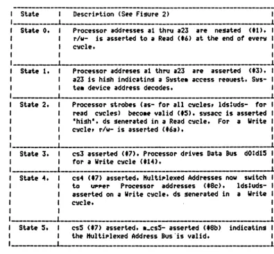
[image:15.618.81.477.128.495.2]1 State I Description (See Fisure 2) I
• ____________ 1 ________________________________________________________ 1
1 State 6. 1 cs6 asserted. iorc- or iowc- Iccerted for access to 1
l i t h e Ti.er or UART. 1
1 ____________ 1 ________________________________________________________ 1
1 State 7. 1 cs7 asserted. No action. .1
1 ____________ 1----____________________________________________________ 1
1 State 8. I csS asserted. No action. 1
I 1 I
1 ______ - 1 ______________________________ 1
State 9. cs9 asserted. Ho action.
1 ____________ 1--_____________________________________________________ -1
1 State 10. 1 cliO asserted. csl0 .enerates dtack- to the 68000. 1
1 1 I
1 _____
-.1._________ _ ___________
_ __
11 State 11. I No action. 1
1__ __ __
1__________________________________
_1I State 12. I Cvcle ter.inates. Ne.ate III strobes (.12). Hetate I
1 I all Clock States (.ll). Slave keeps Data bus valid I 1 I until til. Hetate Data Bus on a Write CYCle (.15). I
1 I I
• ____________ 1 ___________________ .. ___________________________________ 1
Table 1 - Svstea Access Stat.e Flow cont'd
[image:16.620.88.471.147.583.2]os-Ids:
uds-
rlw-
m_rlw-01:23
mo12:23
cs3
I
-
-,
I ,
-' -' -!
.~=--<!)
, I
, '-J,.',
, I '
m_preq-~
__
~~~~~~~======~~cs_walt-
~!~
____
~~'1~~~~~
__~~
m_wa
It-m_a0:7
cs4(mux)
cs5
(m_cs5- )
dtack-
___
--l:~___
~-~:~:-,-I'r
I I
,
'
·1 '
access::
---Jo..&-:4
i
,
I
access:'
I~I--E®-=-H ----~. :--"'--3~~
[image:17.634.113.559.149.725.2]®
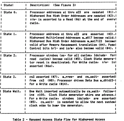
1 State: I Description: (See Fi~ure 3) I 1 ______________ 1 ______________________________________________________ 1 I State O. I Processor addresses al thru a23 are ne~ated (t1).1
I I Hi~hspeed Bus Hi~h Order Addresses are ne.ated (t2).1
I I r/w- is asserted to a Read (.6) at the end of ever~1
I I cvcle. t
I I ,
1 ______________ 1 ______________________________ . __________ ... _ _ _ -1
, State 1. I Processor addreses al thru a23 are asserted (t3).1 , I Hi.hspeedHultiplexed Addresses __ aO:7 beco.e valid.' I I Hi.hspeed Bus Hi.h Order Addresses ._aaI7:23 beeo.el I t valid atter Heaorv Hana.eaent translation (.4). Pa.el I I Control bits b/l- and iol.- also beeo.e valid (.4), I
1 ______________
1---_______________________________________
_ ______
1I State 2. I Processor strobes (as- for all eveles. Ids:uds- fori I I read evcles) becoae valid (.5). Clock State senera-I I I tor reset is deactivated. For Write evele. r/w- isl
I I ISserted (.6a). I
I I I
1 __________
1________ _
__________________
!I State J. I esl asserted (.7). ._prea- and es_wai t- asserted I
I I fro. es3 (.8). Processor drives Data Bus a_dO:dI5-1
, I for a Write evele (.14). I
1 ______________
1___________________________________
_-1I State Wait. One Wait inserted auto.atieallv bv es_wait- follow-I I in. el00. Clock State .enerator skips one advance.1 I For a Write evcle. strobes lds:uds- are asserted I I (.5). es_wait- is ne.ated to allow the next svste.1
I clock ed.e to bu.p the .enerator. I
I , I
I
_______ L______________
_ _______
.1Table 2 - Hanased Access State Flow tor Hi.hspeed Access
[image:18.613.94.499.131.528.2]1
'State: 1 Description: (See Fi~ure J) I
1 _____________ 1 ______________________________________________________ 1
I State 4. 1 cs4 (17) asserted. Hultiplexed Addresses now I 1 I switch to upper Processor addresses <Iec). I
, 1 cs_wait- disabled. I
1 I I
1 ____________ 1 ____________________________________________ 1 I State 5. I cs5 (11) asserted. a_csS- asserted <lOb) indicat- I I I in~ the Hult1plexedAddress Bus 1s valid. Proces- I
I I sor dtack- asserted. 1
, ____________ 1 ________________________________________________ 1
I State 6. I No action. I
I I ,
1 ___________
1____________ _
___________________ .. ______ _1
1 State 7. I Data Bus a_dO:15- captured on a Read c~cle I1 I (110 & 111>. I
1 _____________
1________________________ _ ______ _
___________________ 1
1 State O. I C~cle terainates. Ne~ate strobes (112). Nesate all I I 1 Clock States <11J). Ne~ate a_pres- (116). Nesate 1 1 1 Data Bus a_dO:15- on a Write cvcle (11S). I
t I I
1 ____________
1________________________
_1
Table 2 - Hanased Access State Flow for Hi~hspeed Access cont'd
[image:19.629.88.516.142.488.2]os-Ids:uds·- .
r/w-01:23
m012:23
cs3
bO$-cs_wo
d-cs4 (mux)
cs5, cs6
-..----.j-!..-.I~.
I I I I'
r - - - I - ! J
I I I
I
b_
00:02.3-
---...---4-~oen-
den-
cen- _________
~~~=P~~--~---r~
7
d
7t
I(mr
c-,
mw
c-,
I I I I II ~~~--l:__....JII
) 1 I II
iorc-, iowc-
.:
1 1 Ib _
X 0ck
~
_ _ _
---!-: _ _ _ _
---«-t.$A-.'-t-:
--JI""'-:
--t=-F::-d
to c
k -
:
$ " \ ...!
---,-1--1.1 I
Read access:
1 Ib_ d 0: 15 -
_--....: __
---J$~®~10 J'----<~'i__!
_ _-.,-~~:
'®
access::
I~;6®~:~---~;~
[image:20.621.62.580.84.690.2]---
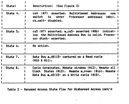
1 I State: I Description: (See Filure 4) 11 _________________
1----______________ _
_____________________________
1I State O. 1 Processor addresses al thru a23 are nelated (.1). I 1 I r/w- is asserted to a Read (.6) It the I
I I end at everV cvcle. I
I I I
1 _________________
1-_____________________________
_ _________________
1 State 1. Processor addreses a1 thru a23 are asserted (+3).1Hanased hish order addresses .,12:23 beco.e validl atter He.orv Hanale.ent translltion (14). Pasel 'Control bits b/l- and io/.- also beco.e valid'
I <t4). I
1 _ _ _ _ _ • __ _
1_________ _____ _ ___________
1I State 2. I Processor strobes ('5- for all eveles, Ids:uds-I
I 'for read cvcles) beco.e valid <.5). Clock Statel , , senerator reset is deactivated. For Write evcle,1
I I r/w- is asserted (.6,). ,
I I ,
1 ___________
...1_____ _____ _
____ . __ .____
_ ____
!I State 3. I csl Isserted
(.n.
bas- and cs_wait- Isserted fro. I 1 I cs3 (.8). Bus arbitration bv the 8289 belun. Pro-II I cessor drives Data Bus dO:dlS- for a Write evclel I I (.14). If .en- is asserted, then the Hultibusl I I co •• and shift relister is enabled. I
1 _________________ 1 ______________________ _ _________________________ 1
State Wait. , One Wait inserted auto.aticallY bv cs_wait- fol-I I lowins cl00. Clock State senerltor skips one I I advance. For I Write evele. strobes Ids:uds- arel
I asserted (.5). cs_wait- is ne.atedto Illow thel I next syste. clock edse to bu~ the Senerltor. I .
, I
_________________ 1______ _ ___________ •••• _________ _ ______ _ 1
State 4
+
Wait. , cs4 <.7) asserted. CI_wait- disabled. Ids- isl I latched to produce aOO. If len- is asserted. then I I the Hultibus Data bus b_dO:d15- is activated boJ', den-. Byte or Word transfers are deter.ined by thel , state ot aOO. Direction is deter.ined by r/w-. ,
_________________ 1 _________________________________________________ -1
Table 3 - Hanased Access State Flow for Hultibus Access
[image:21.612.66.489.88.621.2]I
I St.te: 1 Description: (See Fiiure 4) I
1 ________________ 1 ____________________________________________________ 1
I State 5 t Wait.1 cs5 (+7) asserted. Processor addresses aOl~all,1 I I Hanaled addresses a.12~23 and the state at the .001
I I latch are clocked into the Hultibus Address resis-I I I terse It aen- is asserted, the Addresses arel I I driven onto the Hultibus b_aO:a23-. cen- is also 1 I I senerated and enables the Hultibus coa.and driYer.1
I I I
1. ______________
1__________________ _ ______________________________ 1
I State 6
+
Wait.1 A Hultibus coa.and (towe-, io~, awte- or arde-) I I I is lenerated and butfered to the Hultibusl I I (b_iowc-. b_iorc-, b_.wtc- or b_.rde-) it cen- islI asserted. I
I All coa.and. data and address drivers and I I receivers now re.ain active until b_xack- isl I received fro. the tars.t device. I
___________________ 1_________________________
_ _____________________
-1St.te Last -2. I b_xack- is received fro. the Hultibus. Processor I I dtack- is asserted. Current evcle belins to ter-I I .inate. It the coaaand was lowc-, dtack- asserted I I will nesate it earlier than the other co •• ands. I
I I
__________ 1________
. _________ . ______
1Stat. Last -1. I No action. I
_______________ .1 ___________________________________________ ______ --1
State Last. I Cycle ter.inates. Nesate'strobes (t12). 'Nesate alii I Clock States (+13). Nesate current co..and.1 I Nesate bas- (+16) and Illow other Hultibus "astersl I to be sranted. Nesate Dlta Bus b_dO:15- on a Writel
I cycle et15). I
I I
________ 1 ___ .. ________________________________ _ _ 1 Table 3 - Hanased Access State Flow tor Hultibus Access. cont1d
Hot.: Nu.bers within I()I ref.r to ballooned nu.b.rs in
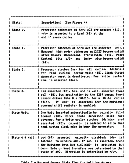
[image:22.613.64.477.117.550.2]3.2.1. Coaaand Generation
See Scheaatic .295014 Pages Sand 1 tor specific IC's ant their loca-tions.
See Fisure 5 - Clock State Generator and fisure 6 - Coaaand Generation for an overview of the losic.
See Appendices G.l throush G.5 tor detailed PAL codes.
The .ajor s~stea ClOCKS on the Processor board (cl00, c200 and c400) are produced by dividing the Raw crYstal oscillator outPUt c50
(PS S IC El) b~ 2, 4 and
a,
respectivel~, b~ a fast tour-bit counter (IC F2)Coaaand Ti.ins relationships are s~nchronized bv the use of a Clock State Generator <Ps S IC H2), which is a 745299 Octal Shift Resister with controls. The clOCK into the Generator is c50 double buffered, so that when shifts are enabled, their outputs will so to the Ihishl state on each edse of the 68000 syste. clock cl00.
The outputs of the senerator are Clock State sisnals, labeled csl to csl0. The 68000 drives its co •• ands, as-, lds- and uds-, relative to Ihish' states of the systea clock cl00. A c~cle beSins at State 0 with negating the address bus and drives the co •• ands at State 2. The first State after as- is asserted is always csl.
The reset input of the Clock State Generator is none other than as- froa the 68000, inverted, thus enablins it on every 68000 CYCle.
The chip has two operatinS states once enabled, "Shift" and "Do
NothinS", controlled by cswait- froa PALPl (PS 5 IC F6). Svste. Accesses do not reauire inihibitins the Clock State senerator, so onlv Manased Accesses (those with address a2l low and Boot off) need con-trol cswait-.
When cswait- is used, it .ust coae before cs4 is shifted in. csl Sene rates RAS-, cs4 .ultiplexes the Dynaaic Raa address lines and csS senerates CAS- on the bank selected by Manased Address aa17.
I
19.6608
Mhz
Osel/Jator
e50
74S240
p.
74S163
OA
DB
DC
OD
carry
elk
74LS163
e100
e200
e400
e800
MuH lbus CJoeks
74S240
~
b_belk-' - - System Clocks Generator
n/e
n/e
n/e
nle
(8 inary Counters)
TImeout Generator
~
enabto-
>-+---IT
e a r r y l - - - - t lmeout
elk
mr
Clock States Generate
as-74LS04
mr
1/00
es3
1/01
es4
1/02
es5
j/03
es6
1/04
cs7
j/05
es8
1/06
es9
j/07
es10
es_wa
It----(
hold-oe
74S299
[image:24.626.97.595.63.731.2](Sh
1ft
Reg ISler)
I\IV-
.nelSoa-1.1.-,
ada-68000
,.Iw-Clock cs3 State cs4 Generator cs5 cs6
...
cs10
Memory
Management
blI-
lolm-m_waJt-: from H 19hspeed Bus
Cycle Acknowledge Inputs Cycle Error Inputs
Managed Addresses Par lty Data & Enables Hlghspeed and Local Commands m_perr- from Hlghspeed Bus
.-I
PA LP0
-}
System Commands) H Ighspeed and Local Commands
PALP3
'--- m_preq- ) Managed Commands -
bas-
-) cswa It-: Clock State Controls Memory
} Management Controls
PALP2 - - berr--
dtack-) ds and bhen
Byte Access Controls
PALP!
~)
~)
Par Ity Controls Onboard Rom Control
3.2.1.1. Status Coaaands
See Appendices G.1 throu~h G.S tor detailed PAL codes.
See Fisure 6 - Coaaand Generation tor la~out of 10lical functions.
The Status ~oa.ands returned to the 68000 are reset-, halt-, berr- and dtack-. halt- and reset- are discussed below.
To acknowledSe the 68000'5 data transfer to the various spaces, dtack- is enabled bv two Clock States: csS ,lwavs and cs10 for S~ste. Accesses and the special aode if an 1-0 Write to Hultibus.
Durins a Hanased Access, dtack- will latch itselt on if no error is present (b~ berrx-). PaSe Control bits b/l- and io/.-, and Hultibus response sisnals aen- and xack coaplete the necessa~ 101ic. The use of cswait- will dela~ asserUnS csS (and csiO)
Durins a Svstea Access, berrx- is actuall~ asserted. but dtack-is now Sene rated bv cs10 and dtack-is not latched.
Error silnals berr- (to the 68000) and berrx- (Extended berr-) are Sene rated independentl~ but share the siae error conditions. The berrx- sisnal is the siaPle ·or· of the four basic errors that can happen: two (2) hardware faults - Tiaeout and Parity Error, and two (2) Heaerv Hanaseaent faults - Protection Error (saaperr-) and Invalid Pale attellPt.
Paritv Error aeans that soaethins is verv wrenl with Local or HishsPeed Heaorv and should be investisated furiher. Ti.eaut, however, can be useful in 10catinS what Hultibus devices and aeaorv Ire actu-allv installed bv touchinl standard lacations and waitins far a response.
The two Heaorv Hanaseaent faults keep the Operatins Svstea and the User honest bv stoppins access to Virtual Addresses that are Pro-tected or .apped Invalid. This sives the Processor bOlrd power for coaplex Operation Svsteas to easilv aanase Heacrv Ind Devices.
See Appendices G.4 and G.l for co.plete lo~ic eauations.
The .aJor S~ste. Access Co •• ands are initiated in two PAls, PALPJ and PAlPO <Ps S IC F6, and P~ 1 IC FS, respectivelv). Svste. Access Co •• ands are those that control the access and direction of data for On-board devices. Host are based on address a23 in the hish state and decode the specific device with a22:a19.
Since access to On-board devices is privilaSed, the 68000'5 Func-tion Code fc2 is sated to enable the co •• and onl~ when the 68000 is in Supervisor state. The User, then, has access to these devices onlv throush Svste. calls or Interrupts,
The current eauation for the sYsacc- and devenab- sisnals are clarified as tallows:
s~sacc- will be low true (Hanased Access) when:
svsacc-
=
as (Address Strobe off, no cvcle)+
as-*
boot-*
a23- (Not in Bootstate and a23 low)t as-
*
boot*
rw-*
a23- (1) devenab- will be low true when: deveanb-=
fc2*
ds*
.23*
a22 (2)+
fc2*
ds*
a23-*
a22-*
a21-*
a20-*
119-*
booi*
rw (3) Product line (1) enables a Hana~ed Acce'SS Write durins Booistateto initialize On-board Dvnaaic Raa. This needs to be done earlv in the Power-on Reset routines to setup valid aeaorv parity tor the Stack area. Up to that point, subroutines could not be called and variables had to be in 68000 reSisters.
Product line (2) enables for SUPervisor addresses startios It OxCOOOOO, "
3.2.1.3. Hanated Access Co •• ands
The .aJorit~ of HanaSed Co •• ands are sene rated in PALP4 (Ps. 1
Ie
F4) and in PALP3 (Ps. 5 IC F6). These co •• ands include! Control Clock States! ._wait-, cswait-.
Hultibus He~or~ and 110 coe.ands; erdc-, .wtc-, iorc-, iowc-, bas-.
Rae and Hishspeed: oe.raa-, we.rael;u-, __ preo-, onbrd-.
Pase Accesses: we •• apx-, en.aapx~.
All of the above co.eands are enabled b~ the "low ' state of
s~acc-, which in turn was enabled b~ the "low ' state of the 68000 address a23. The target bus is selected b~ bll- and iola- froa the
PaSe eap Raas •• preQ- and bas- are Sene rated b~ all of the saae sis-nals, except for the state of bll- (See PALP3).
See Section 3.2.1 for discussion of cswait- and a_wait-.
Hultibus co.eands are not aade active until cs6 is asserted. The seQuence of events for a Hultibus acces are detailed in Table 3.
The 110 Write co •• and is a special case. There are aan~ devices available for the Hultibus and have si.ilar coaaand response lotic for
He.or~, but 110 logic on soae var~ considerabl~ in their coepliance to the Hultibus specification. When doing -an iowc- coe.and, b-xack-asserted b~ the target board will cancel iowc- earl~. bas- and data drivers will sta~ asserted until the noreal end at the c~cle (dtack-asserted and as- negated two (2) hish clock states later).
we.ra.l:u- are directl~ buttered to the onboard Raes during all valid Local or Hishspeed accesses. onbrd- discriainates between Local and Highspeed accesses and controls generatins CAS- to the onboard Raes. oe.ra.- enables the data bufters tor the Local Ra. and the
Hishspeed connector. a_prea- is the overall coe.and that starts soae Local or Hishspeed access.
The PaSe Access coeaands allow the autoaatic updatins of the
"used" and the ·dirt~· status lines for the Pase beins updated. Ever~
3.2.2. Reset Lo~ic
See Sche~atic t295014 PaSe 4.
See Figure 7 for la~out of Reset functions
In order to satisf~ the 68000 reauireaents for I hard Reset, both
reset- and halt- .ust be driven at the saae ti.e.
Hard Reset is senerated b~ "or-ins" several conditions tosether to fora setinit- then buttered throush two open-collector drivers.
Conditions that sene rate setinit- are as tollows:
I
I Reason: I Control: I
1 _______________ 1 ______________________________________ ~ ___ 1
Power On I IC D22 is a voltase coaparator that willi I trip its output when the aain Power Sup-I I pl~ voltase drops below 4.15 Volts. Rl , I and C5 have the ettect ot slow ins the I , turn-on tiae of the Suppl~. ,
,
,
External Reset' External connections on the J2 Connector' , and, throush Juaper Block JB3, the Hul- ,
, tibus b.init-. ,
,
,
Watchdos Tiaerl Prosra.aable Tiaer Channel 1. Usuall~ , / setup to be soae larse count value that , I is restarted ever~ Retresh Interrupt. If/ / the counter is allowed to count all the / I wa~ down, then the Refresh function has , I so.ehow stopped, invalidatins .11 ot / I Local and Hlshspeed Heaor~. I
3.2.3. Boot Losic
See Sche.atic 1295014 PaSe 4. See FiSfJre 8
At power-up or Reset to the 68000, the Processor board is in Boot State. A hardware Reset condition (low-yolta~e cOIParator, external Reset switch or Prosra •• able Watch-dos tiler output) is the si!nal that sets the Boot flip-flop <Ps 4
Ie
H4) and is also buffered to drive reset- and halt- into the 68000, causin! a hard Reset. (This does not affect the 68000 Reset instruction since reset- is then driven b~ the 68000 itself.)This is a te.pora~ condition that allows for loadins the ini-tialization infornation into the 68000 at Virtual .elor~ address OxO. Boot State makes the first Proa address enabled at OxO as well as its noraal S~ste. Access address of OXCOOOOO. Once the Pro. lonitor loads the initial startin! address <soaewhere above OxCOOOOO) then the 900t
r---,
I
+5
Voltage ComparatorI 15K 100K
8211 V+
+5
\ , - - - - 4 hys
~~--1 fhr
Power Level Log ic
tr Igger5 at
+4.75V
10uI 4.l5K out
v-
gnd
L. _ _ _ _ _ _ _ _ _ _ _ _ ~
r---~ I
I
: c. tImer
1
: (from
T
Jmer )
,
7406 :
~ _ _ _ _ _ _ _ _ _ _ _ _ _ _ _ J
r---.l
745240
7406/505
[image:31.624.71.548.44.761.2]In
It
Figure
7 -
Reset
C
!f'CUf-t
In j'~
(from Reset
c frcu
If
above)
+5v
cfrboot-(from
PAlP0)
D S
a
boot
ClK
R
74S74
H4
F
19ure
8 - Boot C
lrcu , .•
reset-3.2.4. Interrupt Losic
There are 7 allowable Interrupt levels into the 68000
cpu.
The hishest (Int 7) is reserved for executins the Refresh Routine ever~ 2 (or 4) .illiseconds. The next level Clnt 6) is a seneral purpose pro-sra.mable output of the AHD 9513 ti.er, as is the Refresh InterrYpt.Level 5 Interrupts are defaulted to the UART for co •• unications. Interrupt Levels 5 throush 1 are hardware wired to the Hultibusr with Ju~pers available to add 6 and 7. All 7 Interrupt sisnals are then latched into a resister CPs 5 IC K6) usins the 68000 s~ste. clock clOO. These Latched sisnals so to a priorit~ encoder CPs 5 IC K7) to provide a three-bit Interrupt code to the 68000 that is s~nchronous
with the s~ste. clock to avoid spurious traps.
Another function of Boot State is to disable all interrupts Just
Llni6- C C
Ini6-Llni7- C C
Int7-b_lni5- 0--0 Ini5-L 0--0 Ini4-L Ini3- c-o Ini3-b_lni2-
0--01nt2-L !nil- 0 - 0 Inil-L!nHJ- 0 - 0
Int0-Int.510--- 0 - 0
Int5-!nt.! Imer2- 0 - 0
Int6-c_re£resh
---l>-
In -t7 (from TImer)741.374
Ocial Reg
,.f.,.
Int7-
Int75-Int6-
Int65-Int5-
Ini55-Ini4-
InH5-Int3-
Ini35-Int2-
Ini25-Inil-
Inil5-CJ( OE
}
boot IPI2-}
Int7.
Ipll-Int6s
Ip10-iniSs lni4s Int3s lni2s
Inils- 741.5148
p,.'O,.'tr
Encod.,.
HuH Ibus Interrupt Seled'lon - J84
Onboord Interrupt Seled Ion - J82
All Interrupts
sync~rono.us wIth Processor
Clock cl00
68000 Interrupt PrlOr!ty Levels
The Series BOA Processor Helor~ Manaseaent unit consists of three address lultiplexors, 5 fast 4096 x 4 static Ra.s, buffers tor High and Low word access and a 512 x 4 PROH prosra.aed to decode Page Access rights.
The processor is provided with a lap that can aap pases of 4K
b~tes an~where in the 16 "b~te address space. During initialization, the PROM Monitor sets UP the Pafe lap tables in a standard wa~ that
.akes all ae.or~ and I/O devices available to user prosrals. User proSrals la~ change these ~aps as desired; however, page 0 and what-ever pages are likel~ to contain the top ot the Supervisor Stack should not be re.apped, otherwise .eao~ refresh .a~ tail.
3.3.1. S~ste. Accesses
Ever~ 68000 bus c~cle accesses soae Virtual .e.or~ location
within the 16 Hb~~e addressing ranse. When address bit a2l is "on", or "hish", then the current c~cle is a S~ste. Access, hence occup~ing the upper 8 "b~tes of available Virtual .e.or~.
--27--The startin~ address for S~ste. Access to the He.or~ Hap is OxSOOOOO. The sisnals ce •• ap- and we •• ap- are !enerated b~ PALPO (Ie
F5). When access into the He~or~ Hap Raas is reauested, the lower address bus into those Raas is aultiplexed b~ the followins table:
I I I
Hanased Access: I S~ste. Access: I Translated Hapl
(a23 Low> I (a23 Hi!h) I Address: I __________________ 1 ___________________ 1 ________________ 1
cxO/cxl a13 xall
a22/cxO a12 xa05
a21 all xa04
a20 a10 xaOO
a19 a09 xa01
a18 a08 xa02
a17 a07 xa03
a16 a06 xa07
a15 a05 xa06
a14 a04 xa08
a13 a03 xal0
a12 a02 xa09
1 __________________ 1 ___________________ 1 ________________ 1
Table 4 - He.or~ Hanase.ent Address Translation
Initiall~, each pa!e of on-board RAH is aapped so that its ph~si
cal and virtual addresses are identical. This' .eans that each se!.ent, startins at sesaent 0, is full~ aapped (up to the li.it of available
.e.or~). Pases are onl~ initialized for context O. Pase protection is set so that both Supervisor and User aodes have Read, Write, and Exe-cute access to e'ler~ ses.ent.
The enable control to the 4K x 4 is per.anentl~ active to allow fast access durins a "anased c~cle. The Write co •• ands are separated into Upper and Lower enables, dependins on address bit al (Sche. pg-1>.
Writing to the Ra. that contains the four Pase Control infor.a-tion is split into two condiinfor.a-tions to !enerate we •• apx-: one for the
nor~al S~ste. access write (we.aapl-) and the other for updatins the used and dirt~ bits (en •• apx-).
The preferred access to the He.orv Hap is via Ions-word (32 bit) .oyes. This tor.at places the Protection Code data bits in the 'Low word', or internal data 31-16, and the PaSe Control and Manased Addresses in the "High word" or internal data IS-0. ConseQuentl~, Hap
o
is located at address OxO, Hap 1 is at Ox4, etc. [image:35.626.86.432.190.421.2]--28--The for.at at the data bus into the Heaor~ Hap is as tollows:
I
I Hap Entr~: 1 S~stea Data:1
1 ___________________ 1 ______________ 1
1 Protection Code: 1
1 __________________________________ 1
1 I 1
I PROT3 I d19 I
1 PROT2 1 d18
I PROT 1 I d17
1 PROTO 1 d16 1
1 ___________________ 1 ______________ 1
I Pa!e Control: 1
1 __________________________________ 1
I 1 1
1 used 1 diS 1
I dirty I d14 1
1 buslloeal I d13 1
1 (b/l-) I 1
I 101 HeaorY I dl2 1
1 (io/.-) 1 1
1 ___________________ 1 ______________ 1
1 Hanased Addresses: 1
1 __________________________________ 1
aa23 dl1
•• 22 dl0
.a21 d9
a.20 'd8_
.a19 d7
.a18 d6
.a17 d5
.a16 d4
aa15 d3
.• a14 d2
.a13 dl
.a12 dO
___________________ 1 ______________ 1
Table 5 - Pase Hap Data Entries
[image:36.612.146.428.123.727.2]--29--3.3.1.2. Context Re~ister
The starting address for a Svstea Access into the Context Resis-ter is Ox880000.
The Context Resister is a one-word field whose bits reflect Yari-ous status inforaation about He_orv Hanaseaent integration, Refreshing of dvna.ic aeaorv and Bus Error generation.
The for.at of data in the Context Register is as follows:
I
1 Data: 1 Function: I
1 _______________ 1 _____________________________________________________ 1
I Read-Write: I I
1 I I
,---______ 1 __ --___ ---_______ 1
dlS I Refresh Enable - When "one", indicates to Slave , boards on the Hishspeed 8us to override Upper
I Addre~s decoding to perait refreshing of Dyna.ic
I nas, if any. d14
I 1
I
I I
I
Parity Enable - When 'one', allows either Local Parity Error detection or Hishspeed Parity Error (a.perr-) to sene rate berr- to the 68000, indicat-ing a bad Read has taken place.
d13 I Context bit cx1. d12 I Context bit cxO.
_______________ l _____________________________ ~ ______________________ 1
Read Only: I Latched Error: 1
I I 1
1-______________ 1 _____________________________________________________ 1
d8 S.8perr- (LON True). Indicates a Protection Code violation.
d7
d6
Parity Error Plrerr- (Low true).
Tiaeout (Hish true). Too auch ti.e taken on a Managed Access (Hultibus or 'Local' raa access). dS Bus Error extention berrx- (Low true). True on any
of the above three error conditions, but is also valid alone when access to a Page aapped "Invalid', that is, aspped as 'Local 1/0', has been atteltPted.
_______________ 1 _____________________________________________________ 1
Table 6 - Context Relister Data Foraat
[image:37.624.71.509.181.761.2]--30--Context bits cxO and cxt provide latched address bits into the Meaory Hap when a Hana~ed Access is initiated. This ~ives the ope
rat-in~ sYstem, like UNIX, the flexibility of switching Heaory Haps easily between processes.
Hardware default enables one context bit, allowing 2 Contexts, each 8M bytes per process. A second context bit, ex!, can be used to provide 4 Contexts, each 4H bytes per process.
--31--The tour 28-pin on-board PROH sockets support the JEDEC standard pin assignments tor ROMs and EPROHs. The Ju.per block JBt (See Appen-dix A) selects address bits a14 and a1S to the sockets.
Default Ju.pers select 2732/2764 type 4K/SK EPROHs and allow expansion upwards to 27128 (16K) and 27256 (32K) type devices.
Access to the first Logical PROH pair is allowed under two condi-tions: one, i~mediatelY after Reset, decodes the PROH 0 startins address at OxOi the second decodes the PROH 0 address at OxCOOOOO.
The PROH 1 address is defaulted to OxCSOOOO at all ti.es.
--32--3.3.1.4. AHD 9513 Ti.er
See 'The Aa9S13 S~ste. Ti.ins Controller Handbook' fro. Advanced Micro Devices for a co.pleat description of all of the functions of the chip.
See Fi~ure 10 for AHD's Function Diasra. of the 9513 Ti.er. 3.3.1.4.1. Introduction
This discussion sives a Quick overview of the functions of the chip that the Series 80A Processor Board aakes use of.
The 9513 isa support device for processor oriented s~ste.s that is desisned ~o enhance the available capabilit~ with respect to count-ins and ti~ins operations. It provides the capabilit~ for prosra •• -able freQuenc~ s~nthesis, hish resolution proSra •• able dut~ c~cle
wavefor.s, retrisserable disitial ti.ins functions. tiae-of-da~ clock-ins, coincidence alarms, cOIPlex pulse seneration, hish resolution baud rate seneration, freQuenc~ shift ke~ins, stop-watch tilinS, event count accumulation and .an~ lore. A variet~ of prosra •• able operation modes and control features allow the 9513 to be personalized for par-ticular applications as well as d~na.icall~ reconfisured under prosraa control.
--33--3.3.1.4.2. Functional Description
See Fisure 10 for AHD's Function Diasrae of the 9513 Tiaer.
The oscillator's freauencs is controlled at the Xl and X2
inter-face pins b~ the S~ste. Clock divided b~ 2, sivins a reference fre-auencs of 4.9152 Hhz. The internal oscillator's output is devided b~
the Freauencs Scalar to provide several sub-freauencies.
The 9513 is addressed b~ the external syste. as two locations: a Control port and a Data port. the Control port provides direct access to the Status and Co~aand Resisters, as well as allowins the user to update the Data Pointer reSister. The Data port is used to co •• unicate with all other addressable internal locations. The Data Pointer reSis-ter controls the Data port addressins.
A.ons the reSisters accessible throush the Data port are the Has-ter Hode resisHas-ter and five (5) CounHas-ter Hode reSisHas-ters. one for each counter. The Haster Hode resister controls the prosra~aable options that are not controlled by the Counter Hode resisters.
Each of the five seneral-purpose counters is 16-bits Ions and is
independantl~ controlled b~ the Counter Hode resister. Throush this
resister, a user· can software select one of 16 sources as the counter input, a variet~ of satins and repetition eodes. UP or down counting
in binars or SCD and active-hish or active-low input and output polar-ities.
Associated with each counter are a Load resister and a Hold resister, both accessible throush the Data port. The Load reSister is used to autoeaticalls reload the counter to an~ predefined value, thus controllins the effective count period. The Hold resister is used to
save the count values without disturbing the count process. peraittins the host Processor to read interaediate counts.
All five counters have the saae basic control losic and control resisters. Counters 1 and 2 have additional Alara resisters and co a-parators associated with thea, plus the extra losic necessar~ for operatiin! in a 24-hour ti.e-ot-da~ .ode.
Each seneral counter has a sinsle dedicated outpin. It .a~ be
turned off when the output is not of interest or aa~ be confisured in
a variet~ of wa~s to drive interrupt controllers, bufters, etc.
--34--A powerful co •• and structure siaplifies user interaction with the counters.
A counter aust be araed b~ onedf the ARH coa.ands before coun-tine can co •• ence. Once araed, the countins process .a~ be further enabled or disabled usins hardware Satins facilities. (The Series BOA Processor necessarilv ties all Gates and Sources to one unchansins state. Sorr~.) The ARH and DISARH coaaands permit software satins of the count process in so~e.odes.
The LOAD co •• and causes the counter to be reloaded with the value in either the associated Load resister or the associated Hold reSis-ter. It can often be used as a software retrisser.
The DISARM co.mand disables further count ins independent of an~
hardware satins. A disarmed counter .a~ be reloaded usins the LOAD co •• and, aa~ be incre.ented or decre.ented usins the STEP co •• and and
mav be read usins the SAVE coaaand. A count process .a~ be resuaed usins an ARM comaand.
The SAVE co •• and transfers the contents of a counter to its asso-ciated Hold reSister. This co •• and will overwrite an~ previous Hold resister contents. TheSAVE co •• and is desisned to allow an accuaulated count to be preserved so that it can be read b~ the-host Processor at
a later ti.e.
Two combinations ot basic co •• ands exist to either LOAD AND ARH or to DISARM AND SAVE an~ combination of cou~ters.
Additional co •• ands are provided to: step an individual counter bv one count; set and clear an output tossle; issue a software Reset; clear and set special bits in the Haster Hode reSister; and load the Data Pointer reSister.
--35--3.3.1.4.4. CadI inc Operatin~ Hodes
The 9513 has been hardware confisured to provide a variety of
services on the Series 80A Processor board. Two (2) of the channels are dedicated Baud rate generators, using Haster Hode D, and do not !!enerate interr~,pts. Two (2) other channels 'Jse Hode A to toggle their associated outputs and provide interrupts to the 68000 at level 7 (for refreshins D~na.ic Rams) and level 6 (user program.able). The
interrupt routines aust set the output inactive and leave the count
run free to interrupt again at the proper rate (ever~ 2 .illi-seconds for INT 7~ for exa~ple).
The fifth channel can be confisured to pulse the 68000 Reset
whenever the count reaches zero. This is called the Watchdog Tiaer
function. It is aeant to be used in an operating s~ste. that .onitors the Refresh counter inte~rupts and reloads the Count into the Watchdog Tiaer. If the operating s~ste. hangs and no longer services these, then the Board will auto.aticall~ Resets.
Channel 2 of the 9513 is the onl~ one buffered to a Juaper
allow-ing connection to an~thing. Its default is to level 6 interrupt. Channel 1 is the Watchdos Tiller; channel 3 is the Refresh Ti.er connected to level 7 interrupt. Channels 4 and 5 are the Baud rate generators.