materials
Yameng Cao1, Alexander J Robson1, Abdullah Alharbi2,
Jonathan Roberts1, Christopher S Woodhead1, Yasir J Noori1, Ram´on Bernardo-Gavito1, Davood Shahrjerdi2, Utz Roedig3, Vladimir I Fal’ko4 and Robert J Young1
1Physics Department, Lancaster University, Lancaster, LA1 4YB, UK
2Electrical and Computer Engineering, New York University, Brooklyn, New York
11201, USA
3School of Computing and Communications, Lancaster University, Lancaster, LA1
4WA, UK
4National Graphene Institute, The University of Manchester, Manchester, M13 9PL,
UK
E-mail: [email protected] and [email protected]
July 2017
Keywords: Physical unclonable function, TMD, optical measurement, photolumines-cence, security
Abstract. The ability to uniquely identify an object or device is important for authentication [1]. Imperfections, locked into structures during fabrication, can be used to provide a fingerprint that is challenging to reproduce. In this paper, we propose a simple optical technique to read unique information from nanometer-scale defects in 2D materials. Imperfections created during crystal growth or fabrication lead to spatial variations in the bandgap of 2D materials that can be characterized through photoluminescence measurements. We show a simple setup involving an angle-adjustable transmission filter, simple optics and a CCD camera can capture spatially-dependent photoluminescence to produce complex maps of unique information from 2D monolayers. Atomic force microscopy is used to verify the origin of the optical signature measured, demonstrating that it results from nanometer-scale imperfections. This solution to optical identification with 2D materials could be employed as a robust security measure to prevent counterfeiting.
1. Introduction
Physically unclonable functions (PUFs) provide a method to generate secrets for unique identification or cryptographic key generation [2]. Instead of storing the secret in digital memory, or asking a user to provide it, it is derived from a physical characteristic of the system. A PUF can be constructed in various ways, including scattering patterns
of an optical medium [3] or chip-specific transistor switch delay variations [4]. The assumption is that the secret cannot be copied, as it is bound to a physical entity which cannot be cloned. Furthermore, it is assumed that the probability of finding two devices with identical physical characteristics is very low.
Existing PUFs have limitations, as they are often difficult to produce, and more importantly, there is no guarantee that they cannot be cloned. Arbiter PUFs, Ring Oscillator PUFs, XOR PUFs, Lightweight Secure PUFs and Feed-Forward PUFs have all been attacked using machine learning techniques [5]. To address the shortcomings, the research community has looked at variations in nanoscale devices [2]. These include the use of memristors [6], fabrication variability in magnetic random access memories [7], unique characteristics in carbon nanotube transistors [8] and phase change memories [9]. These solutions vary in the practicality of implementation, however, they are not sensitive to the smallest imperfections at the atomic scale. This is important because at the lower limit of physical size, cloning of a physical entity requires identifying the chemical makeup as well as dealing with the probabilistic nature of quantum mechanics. Atomic scale imperfections, such as defects in a crystal lattice represent this category of entities. In 2D materials, vacancies, impurities, grain boundaries and other structural defects, lead to spatially varying contributions from excitonic complexes that complicate the photoluminescence. Though spatial non-uniformity could prove detrimental to optoelectronics, the fact that these variations originate from atomic level defects is an advantage for implementing unique optical identifiers, using transition metal dichalcogenides (TMDs) monolayers as optically varying physical unclonable functions (OPUFs).
Spatial inhomogeneity in the photoluminescence (PL) of TMD monolayers, depend on the method of synthesis. Mechanically exfoliated flakes exhibit the highest uniformity while flakes grown by chemical vapor or physical vapor transport are non-uniform in general, due to impurities and defect induced doping. In this work, we demonstrate a method to extract information from the photoluminescence of tungsten disulphide WS2
2. Method
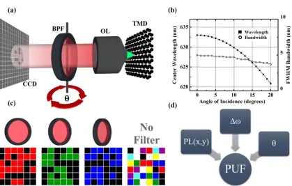
Figure 1: Extracting unique information from 2D materials. (a): Measurement apparatus, in which the photoluminescence from a monolayer TMDC is collected by an objective lens (OL), selectively transmitted through a rotatable optical bandpass filter (BPF), finally imaged on a CCD sensor. Angular orientations of the BPF determines the center-wavelength of its pass band, which varies with incidence angle as shown in (b). (c): Concept of the angular selective transmission. Changing the BPF angle lights up a random subset of pixels on the CCD; red, green and blue conceptually correspond to positions on the monolayer TMDC that emits in differing energy ranges. When no filter is present, all energies are picked up. (d): The BPF angular orientation θ, the corresponding BPF bandwidth ∆ω, and the spatially varying photoluminescence of the monolayer TMDC PL(x,y) makes up the physical unclonable function.
Our concept of extracting unique information from the bandgap of 2D materials is remarkably simple, as depicted in Figure 1(a). A lens collects the photoluminescence from a monolayer TMD, a rotatable optical band-pass filter (BPF) selects a wavelength-range of emitted photons based on its angle dependent transmission wavelength λ(θ) and bandwidth ∆ω(θ), then the transmission is mapped by a charge coupled device (CCD). Direct band gap single atomic layers of the TMD family have shown tremendous potential for applications in optoelectronics [10, 11], quantum photonics [12, 13], spin and valley spin physics [14]. However, to extract unique information efficiently for optical security applications [3], high internal quantum efficiency ηq would be required
shown that it is possible to improveηq especially at room temperature, which is limited
by non-radiative processes. For the scope of this paper, we chose to study WS2 for its
high ηq at room temperature [20] without enhancement. A light source, for instance a
laser or a lamp illuminates a region of the sample containing monolayer WS2, generating
photoluminescence via above-band excitation.
We define the angle of incidence θ ordinarily as the angle which the transmission from the lens makes with the normal to the filter interface. The angle dependent properties of the BPF is illustrated in Figure 1(b), where we firstly find a blueshift in the transmission wavelength λ then also a narrowing of the full-width at half-maximum transmission bandwidth ∆ω, as the angle of incidence is varied. This stems from the fact that at the inter-layer interfaces of dielectric interference filters, the path difference between transmitted and reflected rays reduce with increasing angle of incidence. Correspondingly, the wavelength shift may be described by the following well-known approximation,
λ=λ0
s
1−sin
2θ
n2 , (1)
where λ0 and n denotes the zero-angle transmission wavelength and effective
refractive index, respectively [21]. Transmission measurements of the BPF, manufactured by Thorlabs was not known, though with the transfer matrix method we simulated a generic distributed Bragg structure with similar transmission characteristics as the BPF used in our apparatus. From this simulation we extracted the change in bandwidth with the angle of incidence, as plotted in Figure 1(b).
Changing the angle of incidence selects a specific region on the emission spectrum to be detected by the CCD. Illustratively, colored squares in Figure 1(c) represent light-sensitive pixels on a CCD corresponding to a specific energy range according to λ(θ) and ∆ω(θ). Whenθ = 0, transmission matches the filter specification, but for non-zero angles the transmission blueshifts hence green and eventually blue are being detected. In the absence of any bandpass filter and specular reflections due to the excitation source, the camera records a superposition of all energies for each spatial co-ordinate (x, y). Hence pixels are white if photons of all energies arrive, purple if only red and blue arrive, etc. It may seem possible to take the no-filter image and algorithmically extract the red, green and blue constituents of the emission spectrum, enabling reverse engineering of λ(θ). However in practice, for the monolayers we have tested in this work, the bandgap variation in wavelength is on the order of a few nanometers, or tens of mili-electronvolt in energy, i.e. sufficiently small that the color filters in a CCD would not be able to differentiate between the emission energies.
We prepared samples of WS2 using mechanical exfoliation as well as chemical vapor
deposition was carried out at 950◦C on p+ silicon substrates with 285 nm thermally
grown SiO2, using optimized chamber conditions that allowed large monolayer flakes to
be obtained [22].
3. Results
3.1. WS2 from Mechanically Exfoliation
Defects can degrade the optical quality of monolayer emitters, potentially harming the efficiency of optoelectronic devices. For authentication purposes as a PUF, however, atomic level disorder is a bonus. Defects that tend to increase the spatial inhomogeneity in photoluminescence, the distribution, density and variety of which all contribute to the structural complexity of the optical PUF. We found that the variation in emission energy with filter angle is more pronounced with CVD flakes, though sufficiently large area exfoliated flakes may also be suitable for this application.
In Figure 2, we excite an exfoliated monolayer WS2 on PDMS with 532 nm laser,
Figure 2: (a): 50x Optical image of the exfoliated WS2 flake on PDMS. µ-PL map of
this flake was recorded with 532 nm excitation and 100 µW excitation power at 300 K. The integration time for each pixel is 0.5 seconds. We took spectra from each map co-ordinate and used a Gaussian fit to determine the peak intensity (in counts per second) and the peak wavelength (in nm), plotted in (b) and (c) respectively. In (d), (e) and (f) we applied a rectangular function that selected pixels with peak wavelength falling within a certain band. In all cases the scale bar corresponds to 50 µm.
Next, we applied a rectangular function that zeroed the value of all pixels except those with a peak wavelength falling within a specific range, approximating the effect of an ideal optical bandpass filter. Changing this filter wavelength range then simulates different angle of incidence, as we described previously. This simple function highlights the PL spatial variation within a monolayer and by changing the detection spectral window, corresponding toθin Figure 1(a), different spatial regions can be turned on and off. We showed three spectral windows in Figure 2(d)-(f), corresponding to increasing the BPF incidence angle. This simple function takes into account the peak wavelength as well as the gradient of spatially varying intensity, but it exaggerates the differences between each filter orientation for visual effect. In practice, the difference from one angle to the next is less obvious, since the transmission band picks out a range of wavelengths, rather than only those with peak wavelength in the window.
[image:6.612.80.506.91.375.2]or Mo vacancies could lead to unintentional p-doping. Bandgap renormalization occurs as a result of the doping, as confirmed by the shift in peak emission wavelength across the sample, depicted in Figure 2(c). Adatoms can also lead to similar doping effects, as demonstrated by several studies [26, 27].
3.2. WS2 from Chemical Vapor Deposition
The CVD growth mode is based on a bottom-up crystal nucleation on a target substrate. While other bottom-up synthesis methods exist such as atomic layer deposition [28], pulsed laser deposition [29] and physical vapor deposition [30], crystal size and the quality of the flakes are limited in general compared to CVD. Quality of flakes grown using CVD is heavily dependent on reaction kinetics, which is varied and lead to immense difficulty in reproducing the same growth conditions across different reactors. Monolayers synthesized by chemical vapor growth have defective properties that depend on the types of substrate being used, lattice mismatch at the material-substrate interface, thermal stability and chamber conditions. In addition to point defects, CVD grown monolayer TMDs also exhibit one-dimensional defects, such as agglomerations of sulfur vacancies in a line [31, 32], grain boundaries [33, 34] and dislocations [35, 36].
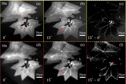
Figure 3 shows the images recorded using filter-angle modulation, for a selected WS2
flake. In each case, PL was imaged through a bandpass filter, Thorlabs FLH633-5, center wavelength 633 nm and bandwidth 5 nm, attached to an angle-variable mount, following illumination using a 450 nm laser at an angle. Laser power density is approximately 3 Wcm−2. In this arrangement, the microscope effectively operates in darkfield mode. The objective lenses used were an Olympus long working distance 50x and a Zeiss 10x. The 10x images were deliberately cropped to highlight the same flake as recorded using the 50x objective lens. Lastly the CCD is a thermoelectrically cooled Sony ICX825 sensor array.
Once θ is set to 0◦, we focused the image under brightfield white light illumination first, then with only laser illumination an image is acquired. As the BPF transmits a narrow band centered at 633 nm atθ = 0, only the single layer WS2 photoluminescence
for each θ is extracted, into a four-dimensional matrix I(x, y, θ), where I denotes the pixel value. Then, for each I(x, y, θ) image in the series, I(x, y, θ0), I(x, y, θ1, ...), the
difference I(x, y, θn)−I(x, y, θ0) was found, where n is the index of an image in the
[image:8.612.81.501.183.464.2]sequence. We then repeated the entire procedure from acquisition to analysis for the 10x objective lens.
Figure 3: Angular-dependent PL images of WS2 monolayer flake, excited by 450 nm
laser, collected using 50x (a)-(c) and 10x (d)-(f) respectively. From left to right: 0◦ with arrows indicating dark spots, 15◦ with arrows indicating bright lines, then intensity differences between 0◦ and 15◦ with arrows indicating the area around nucleation.
quantum confinement. Their origins are unknown to us at present and will warrant further investigation. Though already visually clear, the pixel difference maps in Figure 3 highlight the effect of filter angle modulation, showing the blueshifted emission from surface defects. The fact that we can image these defects even with a low magnification objective lens implies that our system for unique information extraction can potentially be simplified into one with much lower overhead.
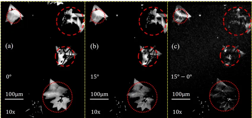
Figure 4: Angular dependent PL images of WS2 monolayer flake, excited by 450 nm
laser, imaged by a 10x objective lens, showing multiple flakes in the field of view that respond to rotations of the bandpass filter. Red circles highlight flakes that showed the most pronounced changes. (a) 0◦ , (b) 15◦ and (c) intensity differences between 0◦ and 15◦.
Other areas on this sample also displayed similar filter angle dependent photoluminescence. We once again show the images taken with the 10x lens in Figure 4, except with a larger image area. In this case we highlight three other emissive areas in the vicinity of the one previously investigated. Structures similar to the grain boundaries identified before exhibit blueshifted photoluminescence detected using only higher BPF angles (θ= 15.0◦, λ = 626.1nm, ∆ω= 4.1nm). We identify two flakes containing line defects that behaved in this way. In contrast, the image signal detected from areas on the domains away from the “lines” attenuate with increasingθ.
Figure 5: Figure 5 Measurements of vertices on WS2 Flake 1 in tapping mode AFM in
air. Scan area 10 µm×10µm
4. Discussion
The key to implementing a real authentication or identification system based on an optical PUF such as the one we described, is to capture the random response or physical characteristics and generate unique fingerprints. So far we have discussed a method to capture the response from 2D materials, based on imaging the fluorescence from structural defects with a bandpass filter at different detection angles. By adding a bandpass filter, we convolute the spatially varying PL of a given monolayer sample with the transmission response of the bandpass filter at different angles, the difficulty of determining each of these two contributions from the resulting convolution determine the overall complexity and therefore strength of the PUF.
The spatially varying PL of 2D flakes is a result of point, line and other structural defects in the crystal as well as dopants, regardless of the method of synthesis. In fact we showed that both mechanical exfoliation and chemical vapor deposition generate flakes exhibiting spatially varying PL. For mechanically exfoliated flakes, edges and vertices inevitably vary not only in their atomic and chemical properties but also in orientation, because the shear transfer from the tape to a single atomic sheet is dependent on uncontrollable crystal lattice dislocations. On the other hand, the spatial homogeneity of flakes synthesized using chemical vapor transport largely depend on nucleation temperature and growth time. It has been demonstrated that long growth time and high nucleation temperature can lead to flakes with high degrees spatial homogeneity, where the distribution of point defects may be controlled by changing the proportion of reactants. In contrast, shorter growth times and lower reactor temperatures reduces the control over spatial homogeneity, producing a large number of defects of varying types, whose distribution maybe based on stochastic processes [37]. The identification of the chemistry of defects requires nuclear magnetic resonance, a complex and expensive procedure. Yet to gain a complete structural map for cloning, all kinds of defects have to be identified and understood exactly on each and every flake. Even then, the dynamic surface energy distribution during growth implies an inherent obstacle to obtain exact geometric replicas. It is sufficient for the context of PUFs, that in the absence of knowledge on the precise atomic and chemical makeup of each monolayer it is not possible to make an exact copy of flakes exhibiting identical optical response.
Micro-lenses such as UV curable epoxy solid immersion lenses can also be integrated to protect the flakes as well as further optimizing the extracting efficiency [39].
5. Conclusion
We report a novel method to implement optically variable physical unclonable functions, using 2D emitters and an angle variable transmission filter. Atomic scale defects have an apparently random distribution that leads to optically measurable unique signatures, comprising of detection wavelength and spatially dependent photoluminescence. It was shown that an inexpensive bandpass filter was sufficient, in terms of transmission variability with angle, to select a range of unique optical patterns from a monolayer WS2.
Forθ close to normal incidence, monolayer emission dominates the optical image and for more oblique angles contribution from line and point defects take precedence. Similar variations were found for other flakes on the same sample, hence for each BPF angle we can select a unique optical signature based on spatially varying PL contributions from each and every flake on the sample. Crystal nucleation and growth generate a continuous spectrum of different geometries even for identical growth conditions, improving the strength of our 2D material OPUF by making it manufacturer resistant. Spatial non-uniform photoluminescence is more pronounced for chemical vapor grown flakes than those created using mechanical exfoliation, as confirmed by AFM that showed a rich distribution of structural defects. Finally, we identify basic security considerations as well as suggestions to improve the detection efficiency of optical signatures. This work paves the way to implementing robust authentication systems protected from cloning at the atomic level.
6. Acknowledgements
RJY and VIF conceived the experiment. Chemical vapor deposition growth was carried out by AA and DS who also optimized the samples for photoluminescence. YC made the mechanical exfoliated sample. YC and AJR setup the experiment and carried out the measurements. YC analysed the data. JR, CSW, YJN, RB-G, UR helped design the experiment. The manuscript was prepared primarily by YC and RJY with contribution from all authors.
7. References
[1] Roberts J, Bagci I E, Zawawi M A M, Sexton J, Hulbert N, Noori Y J, Young M P, Woodhead C S, Missous M, Migliorato M A, Roedig U and Young R J 2015Scientific Reports 516456 [2] Gao Y, Ranasinghe D C, Al-Sarawi S F, Kavehei O and Abbott D 2016IEEE Access 461–80 [3] Pappu R, Recht B, Taylor J and Gershenfeld N 2002Science 2972026–2030
[4] Anderson R J 2008Security Engineering (John Wiley & Sons)
[5] R¨uhrmair U, Sehnke F, S¨olter J, Dror G, Devadas S and Schmidhuber J 2010 Modeling attacks on physical unclonable functions Proceedings of the 17th ACM Conference on Computer and Communications Security CCS ’10 (New York, NY, USA: ACM) pp 237–249
[6] Gao Y, Ranasinghe D C, Al-Sarawi S F, Kavehei O and Abbott D 2015Scientific Reports512785 [7] Vatajelu E I, Natale G D and Prinetto P 2016 Security primitives (puf and trng) with stt-mram
2016 IEEE 34th VLSI Test Symposium (VTS)pp 1–4
[8] Konigsmark S T C, Hwang L K, Chen D and Wong M D F 2014 Cnpuf: A carbon nanotube-based physically unclonable function for secure low-energy hardware design2014 19th Asia and South Pacific Design Automation Conference (ASP-DAC) pp 73–78
[9] Zhang L, Kong Z H and Chang C H 2013 Pckgen: A phase change memory based cryptographic key generator 2013 IEEE International Symposium on Circuits and Systems (ISCAS2013)pp 1444–1447
[10] Wu S, Buckley S, Schaibley J R, Feng L, Yan J, Mandrus D G, Hatami F, Yao W, Vuˇckovi´c J, Majumdar A and Xu X 2015Nature 52069–72
[11] Geim a K and Grigorieva I V 2013Nature 499419–425
[12] Tran T T, Bray K, Ford M J, Toth M and Aharonovich I 2015Nature nanotechnology 1137–41 [13] Ye Y, Wong Z J, Lu X, Ni X, Zhu H, Chen X, Wang Y and Zhang X 2015Nature Photonics 9
733–737
[14] Wu Y, Tong Q, Liu G B, Yu H and Yao W 2016Phys. Rev. B 93(4) 045313
[15] Gan X, Gao Y, Fai Mak K, Yao X, Shiue R J, Van Der Zande A, Trusheim M E, Hatami F, Heinz T F, Hone J and Englund D 2013Applied Physics Letters 103181119
[16] Wu S, Buckley S, Jones A M, Ross J S, Ghimire N J, Yan J, Mandrus D G, Yao W, Hatami F, Vuˇckovi´c J, Majumdar A and Xu X 20142D Materials 11
[17] Amani M, Lien D H, Kiriya D, Xiao J, Azcatl A, Noh J, Madhvapathy S R, Addou R, KC S, Dubey M, Cho K, Wallace R M, Lee S C, He J H, Ager J W, Zhang X, Yablonovitch E and Javey A 2015Science 3501065–1068
[18] Wang Z, Dong Z, Gu Y, Chang Y H, Zhang L, Li L J, Zhao W, Eda G, Zhang W, Grinblat G, Maier S A, Yang J K W, Qiu C W and Wee A T S 2016Nature Communications 711283 [19] Alharbi A, Zahl P and Shahrjerdi D 2017Applied Physics Letters 110033503
[20] Mak K F and Shan J 2016Nat Photon 10216–226 [21] Baumeister P W 2014Optical Coating Technology (SPIE)
[22] Alharbi A and Shahrjerdi D 2016Applied Physics Letters 109193502
[23] Magda G Z, Pet J, Dobrik G, Hwang C, Bir L P and Tapaszt L 2015Scientific Reports 514714 [24] Zhou W, Zou X, Najmaei S, Liu Z, Shi Y, Kong J, Lou J, Ajayan P M, Yakobson B I and Idrobo
J C 2013Nano Letters 132615–2622
[25] McDonnell S, Addou R, Buie C, Wallace R M and Hinkle C L 2014ACS Nano 82880–2888 [26] Chen X, Zhong L, Li X and Qi J 2017Nanoscale 92188–2194
[27] Tedstone A A, Lewis D J and OBrien P 2016Chemistry of Materials 281965–1974 [28] Tan L K, Liu B, Teng J H, Guo S, Low H Y and Loh K P 2014Nanoscale 610584–10588 [29] Late D J, Shaikh P A, Khare R, Kashid R V, Chaudhary M, More M A and Ogale S B 2014ACS
Applied Materials & Interfaces 615881–15888
[30] Liu H, Antwi K K A, Chua S and Chi D 2014Nanoscale 6624–629
[31] Han Y, Hu T, Li R, Zhou J and Dong J 2015Phys. Chem. Chem. Phys.173813–3819
035301
[33] Lin J, Pantelides S T and Zhou W 2015ACS Nano95189–5197
[34] Lehtinen O, Komsa H P, Pulkin A, Whitwick M B, Chen M W, Lehnert T, Mohn M J, Yazyev O V, Kis A, Kaiser U and Krasheninnikov A V 2015ACS Nano 93274–3283
[35] Azizi A, Zou X, Ercius P, Zhang Z, Elas A L, Perea-Lpez N, Stone G, Terrones M, Yakobson B I and Alem N 2014Nature Communications 54867
[36] Zou X, Liu Y and Yakobson B I 2013Nano Letters 13253–258
[37] Govind Rajan A, Warner J H, Blankschtein D and Strano M S 2016ACS Nano 104330–4344 [38] Noori Y J, Cao Y, Roberts J, Woodhead C, Bernardo-Gavito R, Tovee P and Young R J 2016
ACS Photonics 32515–2520