MAINTENANCE.MANUAL 7370/l.48 .MEMORY
"Informati:1n contained herein is disclosed in confideric.e and may not be duplicated in ·full or in part . ..:l;>Y ·any person without prior
writter~ approyifl· of the computer Products Divisioh... Its sole purpose is to provide detaiI'ed. . .,.informat±on to maintain and repair the a·e's:cribed ·equipment. The use of this documen't for o~her ·purposes is specifically
prohibit~d." · - ·
COMPUTER PRODUCTS A Division
942691-002 Rev. A
of Electronic Memories and Magnetics corporation 3216 W. El Segundo Blvd.
Sect. I
1-1 1-2 ·:.1-3
. ,_
.. ·· .. :. 1-4
1-5
1~7
1~8 '<. 1-9
TABLE OF CONTENTS
DESCRIPTCi:ON
General Description
Introduction
System Architecture
Basic Storage Modu2e PWBA (BSM PWBA) Part No. 942945-001
148 Interface PWBA Part No. 942930-001
Storage Protect
Buffered controlled Address (BCA) PWBA Part No. 942940-001
.:Universal Buffer PWBA
I Cycle M Reg EXP .PWBA Part No. 941599-001
BSM. Select PWBA Part No. 942905-001
Sect. II co.nsole Operation and Diagnostic Guide
2-1 '··~\;Introduction 2-2 · Alter/Display
2-3 Diagnostic/Console File Control Switch
2-4 IBM Microdiagnostics
2-5 IBM Macrodiagnostics
2-6 EMM Macrodiagnostics
2-7 Diagnostic Tie Ups
2-8 Error Display
2-9 Address Display
2-10 Four Word Micro-Loop
2-11 RC Mode
Sect. III
3-l. !·.
3-2
3-3
Sect. IV
4-1 4-2 4-3 4-4 Troubleshooting Introduction
General Guidelines
Troubleshooting Guide
Parts Replacement and Adjustments
Line Power Options
DC Voltage Checks/Adjustments
Memory Board/Chip Replacements
Table of
PARA. Sect.
v
5-1 5-2 5-3 .5-4 5-5 5-6 5-7 'FIGURE 1-1 1-2 1-3 4-1 4-2 CHART #1 TABLE 4-1 4-2 4-3contents (Cont.}
DESCRIPTION
Preventive Maintenance Introduction
PM Frequency
Visual Inspection/Housekeeping Electrical Checks
Diagnostics
System Error Logs customer Briefing
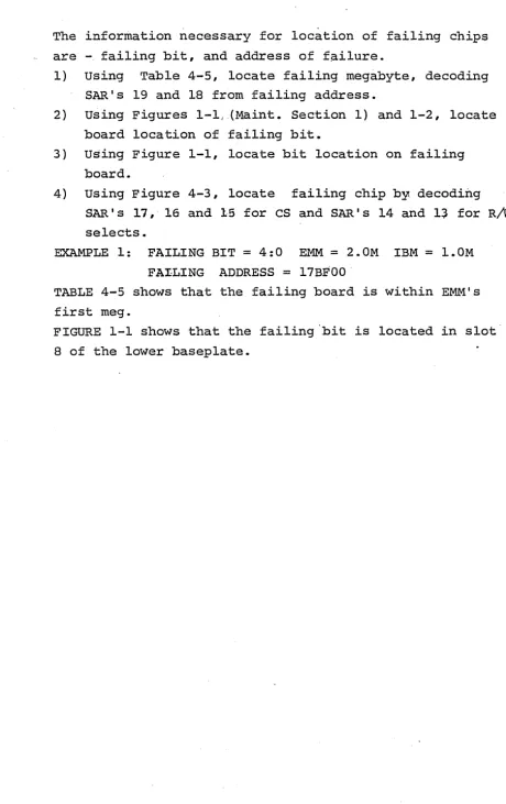
BSM DATA BIT ASSIGNMENT BSM DATA BIT ASSIGNMENT
EMM CPU Upgrade cards EMM CPU Upgrade Cards
ADDRESS1SAR BIT.TESTED CHART
148 Interface Board
BSM Select PWBA Timing Specifications and Jumper Positions
BCA PWBA Switch Settings
[image:4.617.58.612.54.579.2]SECTION I
GENERAL DESCRIPTION
1-1 INTRODUCTION
The 7370/148 MAINTENANCE Manual was written to facilitate the troubleshooting and on-going maintenance of the EMM 7370/148 Main Memory System. The information ~nclosed is not intended to be a "course outline" or "student theory guide", but rather to provide reference informati'On pecu-liar to the EMM 7370/148 Memory Unit and the attachment
(Upgrade) to the IBM System 370/148 Central Processing
u-nit.Therefore, this manual will not supercede the requirement of the Customer Engineer to have:
a) working understanding of IBM System 370 architecture;
b) good technical/mechanical skills; c) common· sense/rationality.
This manual is divided into sections as follows: A. SECTION I - GENERAL DESCRIPTION
B. SECTION II - CONSOLE OPERATION AND DIAGNOSTIC GUIDE(S)
C. SECTION III - TROUBLESHOOTING
D. SECTION IV - REPLACEABLE SUB-ASSEMBLIES E. SECTION V - PREVENTIVE MAINTENANCE
1-2 SYSTEM ARCHITECTURE
The 7370/148 Memory System is designed to enhance any IBM
.370/148 CPU to a total Main Storage Capacity·of 4.0
Mega-bytes ( 4096K Bytes) ·• The enhancement cons is ts of a· Main
Memory __ ~~~:t-~~9~~a:il:li11.g __ up --~-o _ 4 ._O · Me_gaby~e~_ in 1. 0 Meg
incre-ments, and the CPU upgrade hardware required for expanding
Main Storage addressing and Storage Protect.
The 7370/148 cabinet contains up to (4) four Basic Storage
Modules, each containing 1024K Bytes of memory cards (18
BSM PWBA's) and (1) one Interface card. The 7370/148
ca-binet also contains forced-air cooling arrays for the
BSM's, an AC power controller, and.DC power sources for
all EMM 7370/148 Logic.
The 7370/148 Memory System provides for Storage Protect
memory, which is located in the 01B-A4 array of the IBM
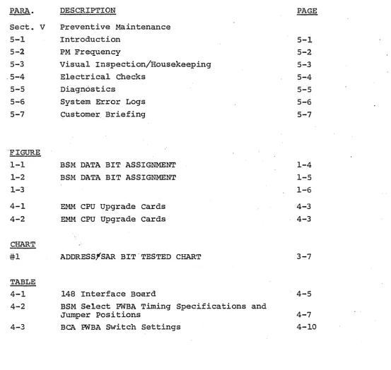
1-3 BASIC STORAGE MODULE PWBA (BSM PWBA) Part No. 942945-001 Each Megabyte of 7370/148 is contained within its own memory bas.eplate, with (18) eighteen BSM PWBA' s required per megabyte. The BSM PWBA is a 4 bit x 128K modul~. On any main storage access to an EMM 7370/148 BSM, all (18) eighteen BSM PWBA's are accessed at once, giving 64 data bits and 8 ECC check bits.
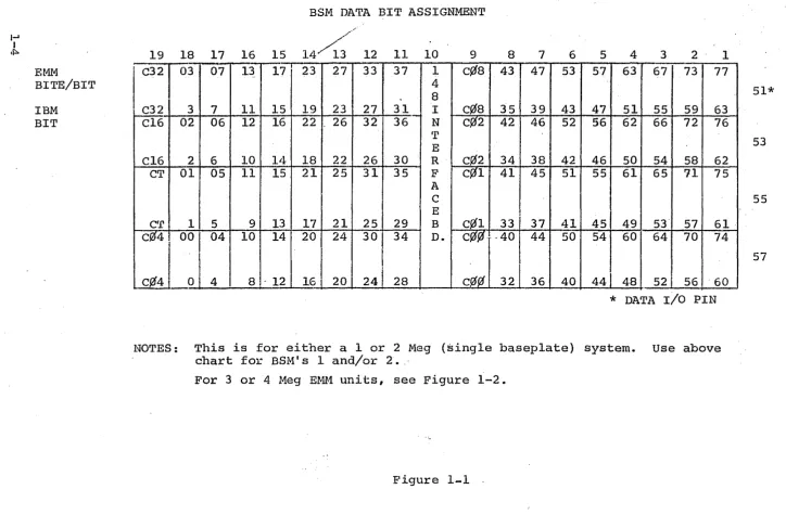
The arrangement of the BSM PW.BA 1 s within each of the (4) EMM Megabyte locations, and the respective bit positions are represented in Figures 1-1, and 1-2. Note: Figure 1-1 is for either a 1.0 Meg or 2.0 Meg System, while Figure 1-2 is for 3.0 Meg or 4.0 Meg versions.
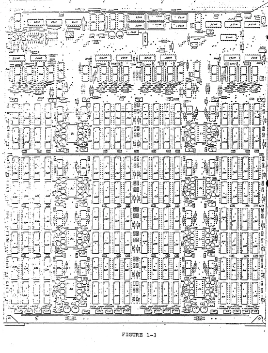
The BSM PWBA has a bi-directional data buss, using MST-2 ·driver/receiver pairs. These devices are replaceable,
lo-cated on·l6-pin dip sockets. See Figure 1-3 for BSM PWBA, and MS'l1 driv~r/receiver locations.
The BSM PWBA recei~es and sends data via the bi,_direction-al buss
dir~ctly
to .·and from the CPU via the interconnect-ing tri-lead cable ·assembly."' Terminations for this data is provided by EMM at the end of the last (highest address-able) BSM installed.I-' I
1f::i.
EMM
BITE/BIT
IBM BIT
BSM DATA BIT ASSIGNMENT
19 18 17 16 15 12 11 10 9 8 7 6 5 4 3 2 1
rl°3
07 13 17 23 27 33 37 1c¢a
43 47 53 57 63 67 73 77 48
C32 3 7 11 15 19 23 27 31 I c¢0 35 39 43 47 51 55 59 63 Cl6 02 06 12 16 22 26 32 36 N cf:{2 42 46 52 56 62 66 72 76
•r
ECl6 2 6 10 14 18 22 26 30 R c¥12 34 38 42 46 50 54 58 62 CT 01 05 11 15 21 25 31 35 F C~l 41 45 51 55 61 65 71 75
A
c E
err 1 5 9 13 17 21 25 29 B c¥11 33 37 41 45 49 53· 57 61. c04 00 04 10 14 20 24 30 34 D.
c¥1¢
-40 44 50 54 60 64 70 74c¢4
0 4 8 - 12161
20 24 28c¢Jl
32 36 40 44 48 52 56 "60*
DATAr/o
PINNOTES: This is for either a 1 or 2 Meg (single baseplate) system. use above chart for BSM' s 1 and/or 2. _·
For 3 or 4 Meg EMM units, see Figure 1-2.
Figure 1-1 .
51*
53
55
[image:8.794.20.744.38.513.2]EMM
BYTE/BIT
IBM BIT
BSM DATA BIT ASSIGNMENT.
19 18 17 16 15 14 13 12 11 10 9 8 7 6
C32 03 07 13 17 23 27
i
33' 37 1 c¢8 43 47 53f 4
8
C32 3 7 11 15 19 23 27 31 c_lla 35 39 43 Cl6 02 06 12 16 22 26 32 36 I c¢2 42 46 52
N T
Cl6 2 6 10 14 18 22 26 30 E c¢2 34 38 42 CT 01 05 11 15 21 2§ 31 35 R C~l 41 45 51
F
·A
CT 1 5 9 13 17 21 25 29 c c¢1 33 37 41 c¢4 00 04 10 14 20 24 30 ·34 E
cf3tf
40 44 50B D.
C~4 0 4 8 12 16 20 24 28 c~ 32 36 40 BSM's 1 & 4 {on 3 or 4 Meg EMM Units) 19 18 17 16 15 14 13 12 11 10 9 8 7 6
rn
73 67 63 57 53 47 43 c}f8 1 37 33 27 23" 4
8
63 59 55 51 47 43 39 35 c¢B 31 27 23 19 76 72 66 62 56 52 46 42 C~2 I 36 32 26 22
N
rr
62 58 54 50 46 42 38 34 c_!2 E 30 26 22 -18 75 71 65
rn
55 51 45 41 c}fl R 35 31 25 21F
.49\
.
A61 57 53 45 41 37 33 cj!l c 29 25 21 17 74 70 64, 60 54 50 44 40
c¢¢
E ·34 30241
20I
441
B
D.
20
I
60 56 52J 48 40· 36 32cf!.%
28 24 16BSM's 2 & 3 {on 3 or 4 Meg EMM units)
5 4 3 2 1
57 - 63 67 73 77
51* 47 51 55 59 63
56 62 66 72 76 53 46 50 54 58 62
55 61 65 71 75 55
45 .49 53 57 61 54 60 64 70 74
57 44 48 52 56 60
5 4 3 2 ' 1 17 13 07 03 C32
51 15 11 7 3 C32 16 12 06 02 Cl6
53 14 10 6 2 Cl6 15 11 05 01 CT
55
13 9 5 1 CT
14 10 04 00
P-ff
4-57 12 8 4 0 ci._4
1-4 148 INTERFACE PWBA Part No. 942930-001
Within each Megabyte location (BSM)°, there is one (1) 148 Interface PWBA, located in Slot 10 (center slot). The 148 Interface PWBA provides signal translation from MST to ECL, chip select generation, 4K addresses for chip addressing, and write controls/write timings. The 148
1-5 STORAGE PROTECT
1-5.1
1-5.2
EMM replaces all of IBM Storage Protect with EMM 7370/148 STORAGE PROTECT. The EMM STORAGE PROTECT UPGRADE FOR ALL 3148 ENHANCEMENTS CONSISTS of (2) PWBA's: the 148 SP
DATA/ADDRESS PWBA, and the 148 SP Array PWBA. Both PWBA's require both the IBM +1.25 VDC and the ·EMM -4.0 VDC up-grade supply be active.
148 SP Array P-wBA Part No. 942915-001
The 148 SP ARRAY PWBA is the actual storage array for all SP keys. The PWBA is an 8 bit x 2K Array. B.its are: Parity bits, data bits 0 - 3, and "fe·tch, reference and change" bits. The arr,ay card will protect both 'IBM and EMM main memory to a ·System maximum of 4. 0 Megs·.
The EMM 7370/148 SP ARRAY is located in slot 01BA4-F2, and is a "4 x 3" card.
148 SP Data/Address PWBA Part ·No. 942910-001
The SP DATA/ADDRESS PWBA interfaces and controls the 148 SP ARRAY PWBA to the IBM 3148.CPU. Both write data and read data is controlled by the. SP Data/Address PWBA. Write timings, X & Y Drives, and card select lines are generated by the 148 SP DATA/ADDRESS PWBA, and sent to the SP ARRAY
PWBA.
1-6 BUFFERED CONTROLLED ADDRESS (BCA) PWBA Part No. 942940-001 Addition of the EMM 7370/148 Main Memory System includes expansion of CPU main storage addressing capability,
diagnostic memory rotation, and "off-line" capability for the EMM 7370/148. The heart of these features is the BUFFERED CONTROLLED ADDRESS (BCA) PWBA. This board gener-ates high-order addresses (M Register 1:1, 1:2, 1:3) by sampling the B Register or Address Buss, according to ac-tive Gate B Reg or Gate Addr Bus to M Reg lines. Also, included within the pre-address assembly logic are paths to the M Reg from the I-Cycle Address Buss for DAT (Dy-namic Address Translation) facilit~es.
SAR's 20, 19 & 18 are generated by the BCA, for use in
=me~ory selects to the EMM 7370/148. SAR is also gated to the· IBM Main s·torage, replacing the IBM generated SAR 18 or "M R~g 1:3 to ECC. 11
·The BCA also controls "M Reg· les-s than ACB" (output of Ad--dr_ess check Boundary comparitor Circuitry) that gives a machine check when a softwaLe-generated main storage ad-dress is greater than the actual high limit of real storage. EMM adjusts the "boundary" when the EMM 7370/148 is "on-line", by holding off the address check circuitry until the ~ Address Check Boundary (ACB) is reached.
1-7 UNIVERSAL BUFFER PWBA
The BCA is fed by signals from IBM panels OlAAl, Ol_AB3, and OlACl. Because of signal transmission charac-teristics due to termination requirements, EMM buffers all critical signals at their source, using two (2) types of UNIVERSAL BUFFER PWBA's. The locations of the Type-001 Buffers are:
OlAAl-G2 and OlAB3-G3 Part No. 942935-001 The location of the Type-002 Buffer is:
01AA1-G3. Part No. 942935-002 Both types of buffers are 11
l wide 11
1-8 I CYCLE M REG EXP PWBA Part No. 941599-001
The I CYCLE M REG EXP PWBA is insta·lled in slot 01BC3-P2. The function of this board is to expand the M Register by 2 bits during I CYCLE PREFETCH operations. M Reg Byte 1, Bits 2 and 3 are developed from the I CYCLE Address, cor-responding to SAR's 19 & 18. The I CYCLE M REG EXP PWBA
1-9 BSM SELECT PWBA Part No. 942905-001 or 942905-002
The BSM SELECT PWBA is a replacement for its IBM
counter-part, and is located on all System 370/148 CPU's, with attached EMM Main Memory, in slot 01BA3-V3. The primary
functions of the board are to generate the IBM memory con-trols, select signals and the selects to each 1.0 Meg EMM BSM. The signal Store (and Stor~) to each EMM Megabyte is
also generated by this PWBA.
During diagnostic testing of the EMM Memory Unit, reloca-ting EMM Memory allows complete tesreloca-ting by the IBM Micro-diagnostics, even though these diagnostics are capable of only testing a maximum of 2 Megabytes of main storage at
a time. By effectively electronically substituting the EMM Memory in 1.0 Meg or ·2 Meg segments, it is possible
to test all main memory with the standard IBM floppy disks. If all microdiagnostics run ~ormally, then the system can be further tested using macro-diagnostics which can be run
with all main memory "on-line.".. This function is performed
by the BSM SELECT PWBA, in qo.nJunc~ion with the EMM DIAG-NOSTIC PANEL. By forcing SAR 18 .. and/or SAR 19 active to
the BSM SELECT generator, the appropriate EMM BSM will~be
selected, instead of the BSM (either IBM's .Qf. EMM's) that would normally be selected according to the state(s) of M Reg Byte 1 Bits 19 and 18. It should be noted that the
actual SAR (M Reg) is unchanged during this operation, theref0re the indicator for SAR 18 (or 19) will not be lit when the 11EMM SAR 1911 is enabled. For further information,
see "EMM DIAGNOSTIC PANEL",
NOTE: There are (2) two types of BS~ SELECT PWBA's: Part No. 942905-001 is for a 1 Meg IBM System, while 942905-002 is for a 2 Meg IBM System. A single jumper
1-10 SIGNAL LEVELS
EMM uses two types of IC components.. Each component type, with their respective voltage levels, are listed below:
MST (Voltage - compensated ECL) High (1) +o.3v to +o.sv Low (0) -0.3V to -0.SV ECL (Non-voltage compensated ECL)
SECTION II
CONSOLE OPERATION AND DIAGNOSTIC GUIDE
2-1 INTRODUCTION
This section is to be used as a reference guide for utili-zation of both the IBM supplied 3148 microdiagnostics, and EMM supplied macrodiagnostics. In addition, the necessary console operations required to properly diagnose system problems concerning the EMM 7370/148 Main Memory are de-tailed within this section. This section used in conjunc-tion with Secconjunc-tion III I TROUBLESHOOTING, should prove to _be
2-2 ALTER/DISPLAY
2-2.l
To use the ALTER/DISPLAY functions,· the IBM CPU must be IMPL'd using the 370 IMPL DISK.l. TO IMPL the System 370/ 148 CPU, the IOC must be loaded first, then the IMPL can be performed. Note: both
roe
load and IMPL are automatic when the IMPL disk is in the 33FD on powering up the CPU.Otherwise, with all CPU switches in their normal positions, and the IMPL DISK 1 in the floppy reader, press the IOC LOAD button and wait for CRT to indicate 'IOC LOADED AND READY', before pressing the "START CON~OLE FILE" key.
Af-ter this, the CRT wil~ request an operator entry in re-sponse to "ENTER IMPL·OPTION11 mess~ge
on CRT display. Cor-rect response for a.370 coreload IMPL is 1
N1
, then the·
. .
11
ENTER11
key. If a good IMPL is performed, the message: 'IPL. CS PATCH ROUTINE THEN CAUSE INTERRUPT.FROM CONSOLE (REQUEST KEY) • will be displayed on the CRT, and the "EXEC CPLTi' in-dicator will be on, on the CPU console. For further IMPL information, see EMM 7370/148 OPS Manual.
Alter/Display Procedure
1. Press the "CPU STOP" push button on CPU console. 2. Press 11MODE SELECT" key.on.console keyboard.
MNEMONIC AND ADDRESS
MNEMONIC
STORAGE AREA ALTER DISPLAY ADDRESS RANGE
Main Storage AM DM 000000 - FFFFFF*
CONTROL STORAGE AS (NOTE
J.)
DS 00000 - lFFFFGENERAL-PURPOSE AG DG 0-F
FLOATING POINT REG. AF DF 0, 2, ~I 6
CURRENT PSW AP DP NONE REQUIRED
LOCAL STORAGE AL (NOTE 1) DL· 00 - 7F
CONTROL REG. AC DC 0 - F
STORE PROTECT KEYS AK DK 000000 - FF FF FF*
NOTES: IBM CE.KEY REQUIRED: TO SIMULATE CE KEY, JUMPER 01AA4-Q4B03
to 01AA4-Q4B08.
*HIGH BOUNDARY IS MOVEABLE, DEPENDING ON AMOUNT OF MAIN STORAGE
2-3
2-3 .1
2-3.2
2-3.3
DIAGNOSTIC/CONSOLE FILE CONTROL SWITCH
This rotary switch allows STORE RIPPLE and Read or SCAN
RIPPLE operations, without having to build machine-language
instructions. To utilize this feature, the CPU must be
IMPL'd with the IBM IMPL disk 1.
To Store Data Throughout Main Storage:
1. CE/OP Toggle switch to CE.
2. Set desired data into rotary switches A - H.
3. Set DIAG/CNSL FILE CNTRL ·sw. to "LOAD SW's A - H. II
4. All other switches to normal, depress "START". Data in rotary switches A· - H will be loaded into all double word locations thro~ghout main storage, until.an ACB
check is obtained. Data to memory is displayed in.··A
Reg, lower roller, position 1.
To Scan Storage:
1. Step 1 as above.
2. Set DIAG/CNSL FILE CNTRL Sw. to "SCAN".
3. All other switches to normal,· depress "START" .
If either the CPU or RETRY ERROR indicators comes on,
place the ERROR CONTROL rotary switch to HARD STORP,
and repeat operation above. Failing address is displayed
in B Reg, upper roller, position 5. Data from memory (SDBO) is displayed in lower roller, position 2.
To cycle a Single Control Word:
The DIAGNOSTIC/CONSOLE FILE CONTROL SW. also provides for
micro-instruction repeat. This allows performing store and
read operations to a single main storage, control storage,
or STOR/PROTECT location.
A. Zero out S P T L REGS
a) Set Roller 2 to Position 3.
b) Set "STORE SELECT'' sw. to ANY LEFT POSITION (EXT REG).
c) Set sw. H to BYTE DESIRED S P T L
B.
d) Set sw's A & B to 00. e) Depress "STORE" PB. ALTER G P R
o.
& 1.a) "STORE SELECT11
SW. to LOCAL STORAGE POSITION. b) Sw. F & G to 00 (GPR
O).
c) Sw. A & B
=
DATA TO BE STORED.d) Sw. H to DESIRED BYTE WITHIN WORD (0, 1, 2 & 3). e) Depress 11STORE" PB ONCE FOR EACH BYTE.
f) .Sw. F & G to 01 (GPR 1)
g) · Sw. A & B to DESIRED STARTING ADDRESS (4 BYTES REQ.). h) Sw. H to BYTE WITHIN THE WORD (0, 1, 2 & 3).
i) Press "STORE" PB ·oNCE FOR EACH BYTE.
NOTE: See Charts 1 & 2 for data & address patterns. C. Set "ACB" VALUE FOR YOUR SYSTEM SIZE (2 BYTES)
(SEE NOTE 1)
a) Set Roller 2 to POSITION 1 (EXT REG OR A REG).
b) STORE SELECT. sw. to ANY LEFT POSITION.
c) Sw. F & G to OA.
d) Sw. A & B to DESIRED VALUE as follows:
~
1. 1024K = 10 03
2. 2048K and above
=
20 03 BYTE BYTE"0" 11111
e) Set sw. H to DESIRED BYTE (0 or 1). f) Press "STORE" PB ONCE FOR EACH BYTE. g) "STORAGE SELECT" sw. to MAIN STORAGE.
D. Set "DIAGNOSTIC CONSOLE FILE" SW. to "EXE CTRL WORD SWS
A+ H".
E. Set -"RATE" sw.in SINGLE CYCLE
F. Set sw's A thru H to the following: NOTE: VIEW ADR. ROLLER 1 POS 5 (B REG)
VIEW DATA ROLLER 2 POS 1 (A REG) 4 8 0 8 1 4 0 3 STORE RIPPLE
6 9 0 4 1 6 0 5 4 1 STORAGE WORD FORMAT
01 STORAGE
WORD
la a a
0 1 ADR.SOURCE
(GPR 1)
co
0 0 0 FETCH
0 0 1 STORE
2
0 1 MODE
Ol=M.S.
lO=C.S.
F 0 3 F 0 3
0 0 0 BRANCH
0 0 STAT.
STORE KEY
READ KEY
I
la
0 Q. DATAINPUT 0
(GPR O)
la
0 0 0 NEXTADR.
,J
G. Set ERROR CONTROL TO DISABLE~:.
Cl 1 0 RIPPLE. INC-.
1 1 RIPPLE DEC.
0 1
NO ADR. UPDATE
3
H. Set RATE SW to PROCESS & press START.
O'O
STAT.
0 0 1 1
I
DISABLEECC
(VAL MODE)
0 0 0 0 NORMAL
NOTES: If System has been successfully IMPL's and 11patched11 ,
2-4 IBM MICRODIAGNOSTICS
2-4.1
IBM provides a microdiagnostic floppy disk with the 3148,
which provides test routines for functional testing of the
3148 CPU and assiciated hardware. It should be stressed
here that these diagnostics are not reliability tests, but
rather are strictly tests for function.··. Intermittant
fail-ures will usually not be flagged with .the microdiagnostics.
The floppy disk ·labeled IMPL DISK 2 BAS/EXO contains the
following diagnostics:
BASICS {BAS) BASIC CPU DIAGNOSTICS
EXTENDED 0 {EX-0)
EXTENDED 1 {EX-1)
EXTENDED 2 {EX-2)
EXTE;NDED 3 {EX-3)
EXTENDED 4 {EX-4) Manual Tests {not used)
BASIC provides the initial checkout of basic CPU hardware
only. The successful completion of BAS is a prerequisite
to running the EXTENDED diagnostics, as the ·facilities tested
by the BAS r9.utines are required to function to operate the
DIAGNOSTIC MONITOR loaded from EX-0.
The EXTENDED diagnostic routines provide increasingly
com-plex test routines, encompassing more and more CPU hardware
as the tests progress. If the EX-0 test section is passed
successfully, 1t is not necessary to proceed in sequence
with the EX-1 thru EX-4 diagnostics; if desired, skipping
to any particular diagnostic is generally possible. Note
however, that all microdiagnostics must be tested before a
system can be assumed "clean" or free of error, previous to
further testing by macrodiagnostics, with the sole exception
of EX-4, which is not required.
Microdiagnostic Run Procedure
To run all micra's, sequentially:
3. All other CPU controls to normal positions, press "START CONSOLE FILE" PB.
4. Enter "D", when CRT displays 'IMPL OPTIONS'; depress "ENTER" key.
5. All micra's are run to completion. To select a specific microdiagnostic:
Note: only EXTENDEDmicro's can be selected.
11. Place IMPL DISK 2 in 33FD.
2. Turn "INTERVAL TIMER" Sw. to "DISABLE".
3. All other CPU controls to normal positions, depress "START CONSOLE FILE".
4. Enter "E", then ."ENTER" key.
5. Place "CPU RATE" Sw. to "INSTRUCTION STEP". 6. When CRT display's following·message:
I CYCLE EACH TEST: y. N. I
Enter "N", then place "RATE" sw. to "PROCESS" . . 7 . . CRT then displays:
I ENTER TEST NAM~: I
Type in desired 4 alpha-numeric character name. ,J • .
8. Diagnostic called in will be-_,automatically initiated. When CPU reaches desired diagnostic location,
follow-ing message is displayed on CRT:
I TEST NUMBER
40 - TEST LOOP 04 - QUIET MODE 20 - SECT LOOP 10 - TEST lD 06 - ERRORS 01 - INSTR Enter Sense SW'
To execute the test, with failure printouts if occurred, enter "40", then "ENTER" key.
To execute the test, with no failure printout, enter "44", the "ENTER" key.
In both cases, the selected test routine is cycled con-tinuously.
2-4.2
2-4.3
of failure. If no test failures occur, floppy disk will continue thru last test ro~tine, then stop.
Loading MBO (Memory Analyzation) Step 1.
2. 3. 4. 5. 6. 7.
Place IBM IMPL DISK 2 in 33FD.
All CPU Switches to normal, press "START CONSOLE FILE 11
key.
Enter IMPL OPTION .11
E11
, press "END" key.
Place "RATE" sw. to "INSTRUCTION STEP".
Respond to 'CYCLE EACH TEST - Y - N' by entering "N", then place RATE SW to PROCESS.
Respond to 'ENTER TEST N~' by entering 11
MBA¢11 •
Test will load and display TITLE and LOOP in-structions, and size of memory to be tested. Set rotary switch "H" to 11
¢
11 for no looping, or 11111for continuous looping. 8. Depress 11
START" key.
MBO test will analyze CONTROL STORAGE, then each megabyte of MAIN STORAGE. Note: the sole determination of the
test-,I
ing range of main memory by MBO is the result of analyzing the FEATURE REG, Byte 2, Bits 0 - 3.
MBO Error Printouts
a) 'EXCHANGE S OlB-XX y y ' .
Where XX = IBM Backpanel Location
Y'I
=
IBM Board/Slot LocationA DBE was detected in the address range covered by the storage board displayed. Two EXCHANGE S messages on the same card indicates 2 bits on that card are failing at the same address.
b) REPLACE S
A solid single bit failure has been detected. The threshold for a solid bit is 256.
2-5 IBM MACRODIAGNOSTICS
2-5.1
The T 148 ( IMPL DISK· 2) Macrodiagnos·tic contains tests for
CPU hardware, Channels, timers, Address Translation (DAT)
Facilities, and STORAGE PROTECT. To operate these tests,
following prerequisites apply:
1. System must have passed BAS - EX-3 normally.
2. System must be IMPL'd with DISK 1.
3. System must be "patched" if EMM Main Memory is to be
included.
4. IOC must be reconfigured as a '148' with "CP/KB"
(con-sole printer/keyboard). See "RC MODE",. para. 2-11.
Procedure for Loading Tl48
1. Place IMPL DISK 2 (IOC/T48) in 33FD.
2. Set CE/OP SW. to CE.
3. Place ERROR CONTROL.sw. to "HARDSTOPu.
4. Perform "SYSTEM CLEAR".
5. Press "START CONSOLE FILE" ·PB.
6. Select IMPL OPTION "T". "~ .. n CRT/KB.
7. Floppy will load, "WAIT" ,lite will come on.
8. Press PA-1 Key on Keyboard •.
9. Hold down "TOD CLK SECURE/ENABLE SET" sw, ·while first
pressing "SYSTEM RESET" PB then "SYSTEM RESTART" PB:
release "TOD CLK" SW.
10.
11.
12.
Repeat above Step 9, except DO CLK" sw.
Press "PA.:..l" key on keyboard.
Display will activate with Tl48
nasties are self-starting.
NOT hold down the \''flOD
Diag-2-6 EMM MACRODIAGNOSTICS
2-6.l
2-6 .1.1
These diagnostics require that the ·Sys.tern 3 70/148 be IMPL' d with IMPL DISK 1, and if the EMM 7370/148 is to be included,·
the system must be "patched".
The following diagnostics may be ·used on the System 370/148 Central Processor, and attached hardware:
DME (E330) ST370 (OLTSEP)
Tl45/T48 (STAND ALONE)
paragraph
MDP (MEMORY DIAGNOSTIC PROGRAM) HDM
2-6.l 2-6.2 2-6.3 2-6.4 2~605
The above diagnostics are stored on magnetic tape, then loaded into Main Memory for use. Rather than explain the operation of these diagnostics, this section will give se-lected "aids" for use, and interpretation of these diagnos-tics. Therefore, i t is assumed that the customer engineer-ing is familiar with the IPL stage and operatengineer-ing procedures of the above diagnostics.
DME (E330)
DME is a CPU utility diagnostic, with a diagnostic monitor providing error logging, interpretation and trace routines.
Full Error Recording/Printing 1. IPL DME
2. When "WAIT" indicator comes on, type the following: I/L330/S.4.5.6.8 (ENTER)
3. When 'WAIT DME' appears on CRT, type the following: E7101.7. XX XX XX 0 0 XX XX XX (ENTER)
STARTING ADDR. 4. Type "B" (ENTER)
ENDING ADDR.
2-6 .1. 2
2-6 .. 2
2-6.3
Stop on ECC ERROR (NO Printout of Errors) 1. IPL D.ME
2. When "WAIT" lite comes on, type:
I/L 330/S.4.5.6.8.13 (ENTER)
3. When "WAIT DME" appears on CRT, type the following: E7101.7. XX XX XX 0 0 XX XX XX (ENTER)
STARTING ADDR. 4. Type 11
B11 (ENTER)
ENDING ADDR.
Routines will loop with no printout of errors.
5. Place CPU "ERROR" sw. to HARDSTOP. All machines wi.il stop on error - with Single ECC being exception.
Press "STOP" key.
. . ~r,.
Install "STOP ON SINGLE ECC" JUMPER (See Para. 2-7_) • Press 11
START11 key. 6.
7.
8.
9. If ECC errors occur, CPU will HARDSTOP. See Para. 2-8 for ERROR DISPLAY~ Para. 2-9 for ADDRESS DISPLAY.
ST370 (OLTSEP) ST370 is basically 370 product line. CPU.
a reliability··diagnostic for the System· It can be IPL'd on any IBM System 370
The main benefit of the ST370 operating system is its ability to fully exercise:
CPU Hardware, Timers, Channels, DAT facilities, control and Main Storages, and Storage Protect.
The best use for this diagnostic is after all other diagnos-tics have been run successfully. Then, this program can be used as a rel~ability test, or to enable the "STOP ON SINGLE ECC" procedure to be used with the system closely resembling actual customer applied useages.
T145/T48 -TSTAND .. ALONE)
System 370/148 must be configured as a 145 with Console
Printer/Keyboard. See RC MODE, pa:r:a. 2-11 .
2-6.4 MDP
2-6.4.1
MDP (Memory Diagnostic Program) is contained on the MTl
Diagnostic U~ility Tape. This program is a main storage
diagnostic routine, allowing full printout/recording of
both solid and intermittant single bit errors, and
map-ping of errors to the device level.
To utilize MDP, the System 370/148 must be IMPL'd with
IMPL DISK 1, and if the EMM 7370 is to be tested, must be ~ -· ·---· ---.. ~~tr
Also, this diagnostic will load only if the IOC is config-.
ured as a 370/145 with console printer(keyboa.a.-d (See RC
MODE,~para.
2-11).----MDP Operating Proc~?ures
-·
Step 1. ·Mount MTl tape and make ready.
2. Enter load unit in~o sw's F, G and H (console)
3. IPL ("LOAD" PB)
4. At "WAIT" state press PA-1 key. Following mes-·
sage is displayed on CRT:
'HARD COPY?'
5. a) If printout is desired, and 370/148 does not
have an attached console line printer, type 'YES'
then press ENTER key. If console line printer
is attached, go to Step 6.
b) Program will then request output device address
(printer). Type 'OOX' (X =device address), then
enter.
c) Press "Restart" k~y on console. Go to St~p 7.
6 •. Press "ENTER" key as "default" option. Printout
will be via console line printer.
'370/145 SER. NO XX XX XX MEM SIZE: XX XX X' '* * * * M.T.I. PROGRAM LOCATOR * * * *
VERSION NUMBER=· 03 • 5 * * * * * ' (where XXX
=
(wherexxx
= IPL DEVICE ID)I ENTER PROGRAM NAME (AS I PROG
x x x x x x
I ) OR'LIST'*
8. Enter 'PROG ~ MDP' ( ~ = space bar)
9. MDP is loaded thru autoloader util~ty. CRT will display:
'PROG MDP LOADED'
I START OF THE M9 MTl MEMORY TEST I
'* A ENTER LOW/HIGH MEMORY LIMITS.'_ .... ,
Respond with correct hex boundaries for desired testing range, then p;r~~: "ENT~R '.' key.
DATA BIT (O - 7) OR C-BIT (c¢¢ ~ c¢T)
..
i}
lK CHIP SELECT ADDRESS (NOT USED)! }
(NOT USED)...
0 en
C)
~
t.n
0
~
~
..
N
('I')
~
~
0 0 0 0
C)
'
~DECODED SYNDROME BITS {S32 Sl6 S8/S4 S2 Sl SO)
(NOT USED)
FAILING ADDRESS
REGION CODE
2-7 DIAGNOSTIC TIE UPS STOP ON SINGLE ECC:
01AB2-N2D07 to 01AB2-M2B08 ENABLE CS WRITE_ (CE __ KEY)__:__ _
01AA4-Q4B03 to B08 NO CF DELAY:
01F-J2B07 to ANY D08 pin. BLOCK PREFETCH:
01BC3-G4B07 to 01BC3-J2B07. DIAGNOSTIC PARITY MODE:
2-8 ERROR DISPLAY
2-8.l
2-8.2
The following assumes CPU has come to HARDSTOP after in-curring a machine check.
To Display MCKB
1. RATE sw. to SINGLE CYCLE
2. Observe STOR 1 CYC indicator. If on, press "START" once.
3. STOR SELECT sw. to MPX OR EXT REGS) 4. Rotary SW .-s. F. & G to 110611
• 5. Upper roller, position 1 = MCKB
To Display MCKA
1. RATE sw. to SINGLE CYCLE
2. Observe STOR ·1 CYC indicator. If on, press 11START11 once.
3. "STOR SELECT" ·sw. to "MAIN".
2-9 ADDRESS DISPLAY
2-9.l
2-9.2
2-18
The following assumes CPU has come 'to HARDSTOP either af-ter a machine check, or due to operator inaf-tervention.
If System has Stopped in Stor 1 Cycle:
M REG should contain valid MS (or CS) address. If not:. 1. Display B Reg (lower CPU roller, position 5)
Bytes 1 - 3 contain MS address, if source is B Reg. 2. Press "START" once, while "RATE" switch is in "single·
cycle" position. M Reg should be loaded with B Reg data if. B Reg was sourced. M.Reg =lower roller, position 1.
If System has·stopped while not in Stor 1 cycle: 1. Display M Reg. If no valid MS Address,
2. Press "START" once while in single cycle mode. 3. Display EXT Reg lB.
a) If Byte 1 Bit 5 • 1, failing microword was a
.I
storage word.
2-10
2-10. l
FOUR WORD MICRO-LOOP
This loop allows store and read operations to two memory locations. This loop will run at normal CPU speeds un-like some loops in the IBM Microdiagnostics which run in . LOCAL STOR/CONTROL STOR mode. Those loops have a. 11dummy11 ·cycle between each control word execution.
Options include storing data in validate mode, which pre-vents ECC corrections and allows writing into Storage lo-cations containing double or multibit errors.
CONTROL WORD CONTROL STATEMENT
ADDRESS WORD
FFF4 490424F3 . STW LSOO, LS02
FFF8 481434F3 STW LSOl, LS03
FFFO 414424Fl RDW LS04, LS02
FFFC 405434Fl RWW LS05, LS03
LSOO = source data, 1st address {STORE) LSOl = source data, 2nd address (STORE) LS02 = source address, 1st address LS03 = source address, 2nd address LS04 = data .dest, 1st address (READ) LS05 = data dest, 2nd address (READ)
Procedure to Run 4-Word Micro-loop
1. Install CE jumper (ALLOW CS ~TRITE) 01AA4-Q4B03 to Q4B08 2. IMPL DISK 1 (11patch11 if EMM 7370 is to be addressed).
3. Depress "SYSTEM RESET" on CPU.
4. Depress "MODE SEL11 key on keyboard.
5. Type "AS FFFO' (ENTER)
6. Type: '414424Fl 490424F3 481434F3 405434Fl' (Depress 'ENTER')
7. Depress "MODE SEL".
8. Type: .:AG-
a·•
.
-VAL VAL
9. Type: · W W W W W W W W
z z z z
.z
z -z z
xxxxxxxx
YYYYYYYY2-20
Z's =address (right-hand justify) for second address. 10. Depress 'ENTER' key.
11. Set RATE ~ single cycle, CHECK CONTROL
=
disable 12. Set P Reg {EXT 04: 1)=
"¢¢"13. Set rotary switches E ~ H
=
11FFF41114. ADDRESS COMP CNTRL
=
SYNC/NORM, ADDR COMP=
controJ.. word address.15. Depress CHECK RESET, CONTROL ADDRESS SET.
16. Press START button while verifying proper operation of loop, then
17. Set RATE
=
Process, depress START2-11 RC MODE
The 370/148 utilizes a CRT display -(125 DISPLAY) and a con-sole KEYBOARD. Optional features include a line printer. These I/O devices are generally assigned as (1) one unit, emulating the console printer/keyboard (3215) used on the 370/145. Alternate assignment may make the console CRT/ Keyboard one device address, and the optional line printer another (if attached).
To reconfigure the I/O devices present on a particular 370/ 148 CPU, the IMPL disk 1 must be loaded. At completion, follow the· operations described below:
1. IMPL with Disk 1 successful~y. 2. "PATCH" system, if desired. 3. On-CRT, press MODE SELECT key. 4. Type "RC", then "enter" key.
5. 33FD reader will locate configuration data. CRT display will show present configuration data. 6. Follow directions on CRT for altering data. 7. To terminate configuration, press PA-3 key.
SECTION III TROUBLESHOOTING
3-1 INTRODUCTION
3-1.1
This section is intended to be a guide for the qualified customer Engineer to troubleshoot and correct system fail-ures associated with the EMM 7370/148 memory system, and the CPU upgrade hardware. Contained in this section is all the necessary information to successfully maintain the EMM memory system.
It mus.t be made cleali' that this manual will not replace the need for pre-requisite training on the 7370/148 memory system, or the necessary familiarity with the IBM.370/148 central Processing Unit.
contents
A. B.
GENERAL GUIDELINES TROUBLESHOOTING GUIDE
3-2
3-2 GENERAL GUIDELINES
The following steps should be verified as being performed prior to determining any specific failing· area or assembly: 1. Normal PM has been performed on the unit, insuring all
power supplies ·are properly adjusted, and an adequate airflow is passing through the baseplate(s).
2. All cables, tri-leads, and harnesses are checked for good routing and seating.
3. A.C .. line voltage is
±
10% of nominal.The following rules should apply whenever a problem situation arises:
1. When replacing any CPU upgrade card, both the IBM, CPU, and the EMM 7370/148 should ~e powered down. Note: by placing the CPU power control panel switch CES to "I/O HOLD", the I/O gear connected to the .CPU will remain powered up. Also, i t may be desired to leave the 7370/
148 memory unit powered up, and only power-off the CPU/ UPGRADE supply when replacing upgrade cards. Use the
CPU/UPGRADE ON/OFF switch on the EMM A.C. control Assem-bly.
2. When swapping cards, be very careful to recognize chang~ ing symptons. If symptoms do not change, ALWAYS put back the original card(s) to original locations. Also, when trying spare boards, place only 1 spare in the unit at a time. DO NOT 0SHOTGUN" SPARES, in an attempt to re-pair problems. Generally, this only results in "digging a deeper hole".
3. Whenever a problem appears to be IBM's, but i t is in an area related to the 7370/148 upgrade, ensure that all signals related to the failure are scoped and verified before calling in IBM. Remember that the upgrade on
3-3
3-3 ... l
3-3 .1.1
TROUBLESHOOTING GUIDE
Problem/Source Determination
Assuming that a red-lite error has occured, the initial de-cision to be made is whether the problem is in the EMM
sup-plied hardware, or the resident IBM CPU. BASIC's generally will detect memory or CPU errors, other than single bit errors. It will locate a solid failing data-bit line by testing "address as data" patterns. Therefore, BASIC's is probably the best diagnostic for starting the determination· process.
On most problems, i t is adviseable _to first test the IBM CPU without the EMM 7370/148 active. This may be easily accom-plished by sw1tching the EMM ON/OFF switch, on the EMM Diag-nostic Panel, to OFF. Another method is t~ power down the EMM 7370/148. (Remember that the upgrade supply must remain on).
With the EMM unit "off-line", ~allow the steps below for de-termining EMM vs. IBM failure source.
Determine Failing Unit (IBM vs. EMM) EMM OFF-LINE I. RUN BASIC 1
. s
A. If no error, next step (II) B. If error:
1. For SAR check, step IVA. 2. For DBE, step IVB.
3. For SBE, step IVC.
4. For STOR/PROTECT, step IVD.
s.
For ALL OTHER FAILURES, notify customer, problem is IBM's.II. RUN EXTENDED's (EX-0 thru EX-3} A. If no error, next step (III) B. If error:
1. For SAR check, step IVA. 2. For DBE check, step IVB.
III. RUN Tl48 (IMPL FIRST!)
A. If no errors, problem is most likely EMM's-Go to Paragraph 3-3.2.
B. If error:
1. For SAR check, step IVA. 2. For DBE:- check, step IVB.
3. For STOR/PROTECT check, step IVD.
4. For ALL OTHER FAILURES, problem is most likely IBM.
IV. TROUBLESHOOTING FAILURES A. SAR CHECK
1. EMM BCA Slipp lies SAR 1
s 20, 19, ·& 18 and SAR Pl. a) Replace BCA location 01AB1-T2, return to
step IA.
b) Chee~ tr±-leads· at 01AB1-T2 thru TS, return to step IA.
c) Check tri-lead at 01BA3-V3J05
(+
MS ADDR 18) return to step IA.2. Determine Failing SAR Line
a) Use Single control Wd. Loop 2-3.3
use chart #1 for address bit location.
b) If SAR's 20, 19, 18 or SAR Pl cause SAR RTY CK.
(.1) Scope affected line for valid levels.
(2) Check affected line for correct source/ destination.
(3) Replace (one at a time) the EMM UNIVER-SAL BUFFERS.
LOC 01AA1-G3 LOC 01AA1-G2 LOC 01AB3-G3
c) If failing SAR line is not SAR 20, 19, 18 or p1 •
...
B. DBE (Double or Multibit Error) 1. On 1.0 Meg. IBM Systems·
a) EMM plugs into 2nd Meg. Port (.unoccupied by IBM). Therefore, DBE's while running IBM only cannot be caused by EMM's data and address cables.
b) Check BCA for a stuck SAR 18,- 19, or 20. c) Check +MS Addr. 18 to ECC for proper
con-nections.
d) Check BSM select card for proper opera-tion, 01BA3-V3.
IBM's BSM select card can be put back into the system to verify function. No wire changes are necessary.
2. On 2.0 Meg. IBM Systems
a) EMM extends (daisy-chains) the address and data lines from IBM's 2nd (HI) Meg. Also, the terminations for these nets are removed from IBM (Ldc. 01BC4-V2) and suitable ter-minators are placed a~ end of net (last EMM Meg BSM).
b) check all EMM tri-leads at 01BC4-V2 thru
vs.
c) check all EM.M. tri-leads at 01BC4-A6 and B6. d) Check for proper seating:(1) Paddle boards at EMM 1st Meg.
(2) Terminator boards at EMM last Meg. (3) Any and all jumper cables from one EMM
Meg to another •
e) Check CPU/UPGRADE P.S. for proper voltage. f) NOTE: failures in IBM 1st (LO) Meg cannot be caused by 2nd Meg (HI) cable or
termina-tor problems. If problems is in 1st (LO) IBM Meg, refer to step IVBl.
CHART #1
ADDRESS (Source Register Content)
00000000 00000004 00000008 00000010 00000020 00000040 00000080 00000100 00000200 00000400 00000800 00001000 00002000 00004000 00008000 00010000 00020000 00040000 00080000 00100000 00200000. 00400000 00800000
SAR BIT TESTED
U/L 1 2 3 4 5 6
7 \
8 9 10 11 12 13 14 15
. 16
17
18
19
20
c.
SBE (Single Bit Error)1. If a solid single bit erro~ occurs in IBM main memory:
a) On 1 Meg IBM systems, EMM has no affect to IBM data I/O for the 1 IBM Meg.
b) On 2 Meg IBM systems, EMM does not connect in any way to IBM's 1st (LO) Meg. There-fore, SBE in IBM's LO Meg. are not EMM caused. Only the 2nd IBM Meg. can be af-fected by EMM as far as SBE are concerned. Note: If the SBE is at all addresses,
(solid' data-line failure) scop~ affected data-line from IBM 01BC4-V2 ·board, to the EMM replacement terminator board. If the net is not contiguous, there would be a
lack of termination at the IBM 2nd Meg., and no path for EMM's data I/O line to the IBM HI port. Che~k affected I/O cable for correct placement.
2. If the SBE is segment-selective, (run MBOeif only 1 slot location per bit is listed as failed, SBE is card sensitive) verify by moving affected stor-age board in IBM 2nd Meg. Re-run diagnostic-check for changed symptom. Problem is probably dead storage chip in IBM memory, if error moves with IBM storage card.
D. STORAGE PROTECT
1. All storage protect is replaced by EMM.
a) If failure is a solid bit-line failure, at all addresses, replace EMM SP Data and Address BD., Loe. 01BA4-C2.
b) If failure is a solid bit-failure at selective addresses, replace EMM SPS Array Bd., Loe. 01BA4-F2.
3-3. 2
are C2P02 (SAR 20), C2P04 (SAR 19), and
C2P05 (SAR 18). If these tri-leads are
loose, the corresponding address to the
EMM Data & Address Board will be active,
skewing the card and segment selects.
d) If above does not correct problem, replace
BCA Bd. Loe. 01AB1-T2. The EMM supplied
BCA Bd. supplies the hi-order memory and
storage key addresses (SAR's 20, 19, 18).
Remember, the EMM upgrade supply~ be
active to operate the storage protect and
BCA logic.
Never remove or replace either EMM Supplied
or original IBM supplied logic or storage
cards with IBM .Q!.. EMM power on. Always power off the CPU and attached EMM 7370/148 main
memory, before changing cards. NOTE: you
may power off the EMM upgrade supply by
switching the u~grade ON/OFF toggle switch
to the OFF.
Troubleshooting EMM Failures
In the previous outline, many modes of failures were examined,
most of which could be caused by the EMM 7370/148 memory unit,
and the CPU upgrade hardware. Remember that. most any failure,
caused by EMM, involving the UPGRADE will probably _show up in
both IBM only and EMM on-line modes. Therefore,
trouble-shooting should alwaxs initiate with verifying proper operation
of the upgrade and attachment hardware in IBM only modes.
Generally, if the IBM CPU runs-ctean-without the
7370/148-mabl-storage unit logically 11active11
, the only hardware left untested
will be the EMM 7370/148 storage unit (ie: BSM boards and 148
Interface Bd.), and the increased storage address range (ie:
the BCA hi-order address generator). Note that the BCA·, and
the BSM SELECT PWBA's are at least 60% tested under "IBM only11
mode. In the case of the BCA, in most configurations, the
3-3.2.1
bit generation, and the corresponding adjustment in the ACB
(+M Reg
>
ACB) hold-off. In the case of the BS~ SELECT, all IBM selects, g~nerated by the card,· have been checked. Theonly remaining logic left unchecked is the blocking of IBM
1 and 2 Meg selects and controls, and the.gating of EMM
se-lect(s) and write controls.
Follow the outline below for troubleshooting EMM failures.
The following assumes that the IBM CPU is error.free with
EMM "off-line·"; but attached.
Note: When .running EQB7 on EX-3, with EMM memory "on-line",
at a total system size of 3 Megs or greater, EQB7 will fail.
If0 the EMM ON/OFF switch on the diagnostic panel is set to
"OFF", the EQB7 failures should disappear.
The reason for the failure is that EQB7 attempts to force
an address exception (MS SAR> ACB) to check for correct
trap routine •. If the diagnostic is run at 2 Megs, with the actual main storage at 3 or more Megs, EMM raises the ACB to the appropriate level. However, because the micro's will
only test to 2 .Megs, no ACB check occurs at a 2 Meg
+
1 address.Locating EMM Failures EMM ON-LINE
I. Place EMM 7370/148 memory "on-line".
II. RUN BASIC diagnostic.
A. If no error, next step (III).
B. If error:
1. SAR check, step VI. 2. DBE check, step VII. 3. SBE check, st~p IX.
4. ALL OTHER FAILURES, return to
test IBM only.
III. RUN EXTENDED Diagnostics
A. If no error, next step IV.
B. If error:
f.
SAR check, step VI. 2. DBE check, step VII.3. SBE check, step IX.
4. STOR/PROTECT check, step VIII.
IV. IMPL, then RUN Tl48
A. If no error, next step (V}.
B. If error:
1. SAR check, step VI.
2. DBE check, step VII.
3. STOR/PROTECT check, step VIII.
V. RUN RELIABILITY (MACRO DIAGNOSTICS) TESTS
(OLTSEP, ST370, E330, etc.)
A. Remove all SBE (chip failures) in 7370/148 unit.
B. ·Operate under margins •
.. , 1. If no further failures are· found, unit
should be fully operational.
2. If failures are s t i l l encountered, return
to step I.
VI. SAR CHECK
A. Replace BCA PWBA.
If no fix, next step. (~eplace original BCA). "
B. Replace Universal Buffer, Lo~. 01AAl~G2.
If no fix, replace original Buffer, then next
step.
c.
Replace Universal Buffer, Loe. 01AA1-G3.-If no fix, replace original Buffer, then next
step.
D. Check all EMM tri-leads at:
01AA1-G2
01AB1-T2 thru TS
01AC1-VSB02
01BA3-V3
E. LOCATE FAILING SAR LINE
VII. DBE
1. use Single Control Wd. Loop, Para. 2-3.3. 2. use Chart #1 for S~...R Lil':IBS/GPRl CONTENT. 3. If failing, SAR is 20, 19, 18 or SAR Pl,
scope affected net back to BCA board.
A. verify proper address function to EMM 7370/148
Verify that all SAR's function both on and off. B. Verify proper data-line path function.
Use Single control Wd. Loop, Para. 2-3.3.
Vary Data to Memory-Check for Bit cross or Bit Malfunction.
c. Verify failing address (address range).
IF FAILURE is in l.EMM Meg only, and another EMM Meg is functional, problem is not I/O cables or addresses 17 ~
~-a) verify function of BSM selects to EMM (at · EMM backplane) •
-b) Verify function of block signals to IBM 1 and 2 Megs. (at BSM SELECT PWBA).
c) verify function of STORE signal at affected EMM_Meg.
d.) Replace 148 INTERFACE BD. in affected EMM Meg. e) Replace affected BSM Bd. (use MBO).
VIII. STOR/PROTECT
If STOR/PROTECT fails only when EMM 7370/148 is ON-LINE_, but runs O.K. when IBM only, the only difference is the amount (address range) df keys required or used in the particular configuration. Theref_ore, if the STOR/PROTECT works at 1.0 Meg, the problem is either a bad key in the
1 to 2 Meg address range, or SAR 18 to the Storage Protect DATA
&
ADDRESS card is not functioning. Refer to Section 3-3.1.1, step IVD.IX. SBE
A. If a SBE occurs:
verify address-range:
a) If all addresses, check affected BSM Board, or Data I/O cable{s).
4-1
4-1.1
4-1.2
SECTION IV
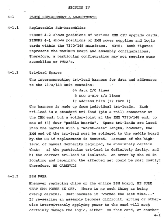
PARTS REPIACEMENT & ADJUSTMENTS
Replaceable Sub-Assemblies
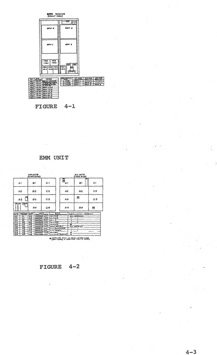
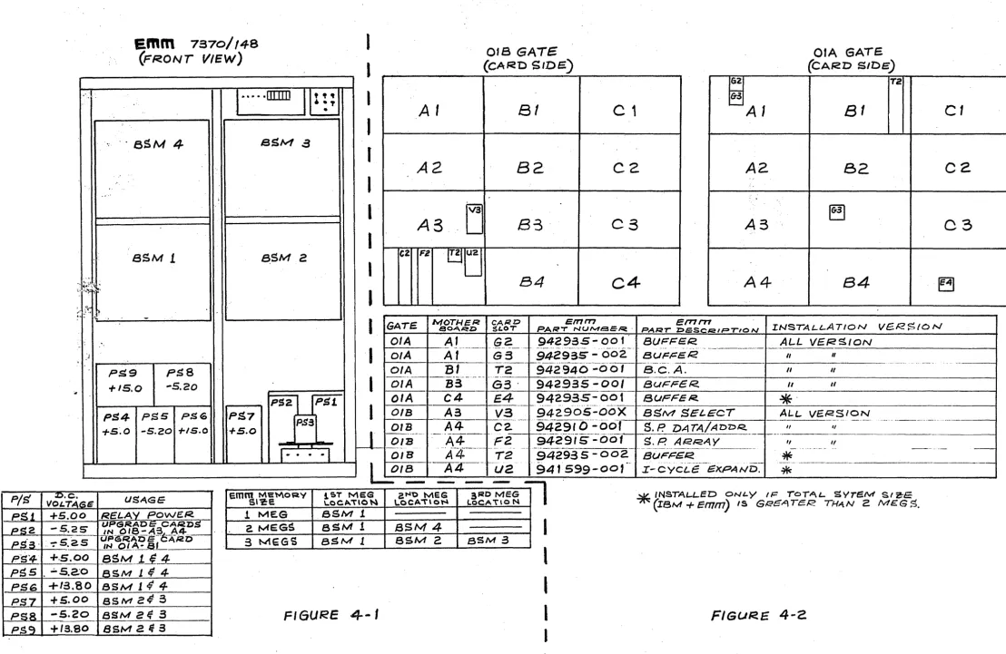
FIGURE 4-2 shows positions of various EMM CPU upgrade cards. FIGURE 4-1 shows positions of EMM power supplies and logic cards within the 7370/148 mainframe. NOTE: both figures represent the maximum board and assembly configurations. Therefore, a particular configuration may not require some assemblies or PWBA's.
Tri~Lead-~pares
The interconnecting tri-lead harness for data and addresses to the 7370/148 unit contains:
64 data I/O lines
8 ECC C-BIT I/O lines 17 address bits (17 thru 1)
The harness is made up from individual tr±-lead~. Each
~
tri-lead is a standard tri-Lead (pin & rail)- connector at
•
the IBM end, but a solder-joint at the EMM 7370/148 end, to one of {4) four "paddle boards". Spare tri-leads are laced into the harness with a "worst-case" length, however, the· EMM end of the tri-lead must be soldered to the paddle board ·by.the CE if replacement is desired. B~cause of the
high-level of manual dexterity required, be absolutely certain that: ·a) tbe particular tri-lead is definitely faulty, and b) the correct tri-lead is isolated. An error by the CE in
locating and repairing the affected net could be most c'ostly! Therefore, BE CAREFUL!
BSM PWBA
Whenever replacing chips or the entire BSM board, BE SURE THAT EMM POWER IS OFF. There is no such thing as being overly careful. Just ·becuase it "worked the :I:.ast time ••• 11 . If re-seating an assembly becomes dif£icult, arcing or
[image:51.626.52.591.48.762.2]one. Remember that data lines from each BSM board
t'.it~
the same ones that IBM uses (ie: data is "daisy-cha~ned" from ·~.; IBM to EMM, not "buffered") for the HI (2nd} megabyte of main memory..
~~ . . When removing or replacing BSM boards, if ,wa~page isen-~ ,.·i .. ~ .
countered, try the following procedure:·
.
· ,, ~ ~·· .,.
...ft I, ~· •· ~ ~~\~:;: ~ •
1) Locate assembly in card-guides.~ Be. sure botnl·~top
2)
3)
.. ·· ..
""·"·
and bottom edges are within guides." "':·\!{·.~.,.,."'1 . '".• •. Slowly slide board in and out, from ·conn,~¢.~o~ ·.,f.?-ce, to about 6" fr.om· connector. ··Assertain
whetif~r.
card, is staying within guides, or~5·· e~gin~ ··o~£·
of.-.~i~h~r
,, • • 1 ... ,,
guide.
,.
. ,. ·~
Slide assembly out about -6,:" fr.om connector .·fat:·e, then firmly ~nd smoothly sn~~~~~~.f~. )?()ard into ~he backplane connector, using your·
-~'"lngertips. ~~ ~9
not miscontrue the abo'l~;.,~th'l:$ ~ ~~~;not, .. a~-ai;'f;.~mpt. '· . "·.~~,.;...~ '':'!··fo,.,k;'.~tlN·~~~ ~;-" :' 1; :l:-.' ;~:.:· ·\ .
to smash the board into the.connector!. Therefore,
picture the relative
1Q~i6n~:·~~,f$~b.'!-i_;h~·;te;tfg~'·:::;:·
EMM CPU UPGRADE CARDS LOCATIONS AND PART NUMBERS
[image:53.623.202.596.54.782.2] [image:53.623.173.610.62.775.2]+1s.ao a Ma.fl
FIGURE 4-1
EMM UNIT
018GATI! OIA. GA.TS
(CAIOD"IDS) (CAJl!D 81Da)
Al Bl Cl l![AI Bl
n
ClA2. 82. C2 AZ 82 C2
AS
r
83 C3 A:3 el C3m·
~o B4 C4 A4 B4 ~...
-.
,, ... ·.
:.:~~1
> {\: )
~ :· I~.. ,,
..
..emm.
7s70/
14a
(FRONT
VIEW)
... IlIIIIJ
...
.
8SM
4
BSM..
..
..
-,.: . '
·asM
1
~SM...
-..
PS9
PSS
+1s.o
-s.20PS2
PS4
PSS
PSG PS7 +5~0 -s.20 +1s.o+.s.o
.
-t
,
.
•
•41•
.a
2
UPS!
P$3
..,
...t:.
.
·J
I
I
I
l
I
I
l
I
I
I
I
·1
I
I
J
A
A
A
C2 F2
GATE.
OIA
Of
A
Of A
,
2
3
[j
a
U2.'
-lv/OT/-1 EI<
a o.o.. "".z:>
Af
018
GATE
(CAr<D
SIDS')
81
B2
B3
84
c
1
C2
c
3
C4
CARD Emrn
$t.OT PAR·r NUl\4Sl:R.·
942985-001
---·- ·-· ., ···----·
___ @_.? __
--9429-35
-"00·2-· ..
A1
G3
01A
GATE(CAF<O S/De)
62 12
~
~A
1
8
1
c
1
A2
82
c
2.
., . .
A3
~
c
3
..
A 4
84
~
efT1rrt
INSTALLATION V6.R$/O N
PAt:C?T Z>E:S~QIP'TIO N
BUF!=ER. ALL V/E.!<SION
' - .. -- ... --··· ···-··-·---·---.. ···- ·--..
·-BUF!=IE.R II II
+---.. - - - -f - - - .. ---·-·· .. _ .... __ - - - -...
_
... --··-..Bl
12
942940
-001 B.C.A. - II II ---····- ... ·-·---. -· -...-·-- -·-- -·-- -·-- -"I~--3··-
···---
····-···---DIA
G3
942935-00/
BUFF/ER.. It tiOIA
C4
E.4
942935--001*
BCJPF'ER.. ···-t-·· ... ... -- ... -- ---· . - - · · - -
1---OIB
A3
V3
94290S-ooX
BSM SELECT ALL. VERSION·---~-..
-94291
o--~'Oot --·-··---__
.. ..,.. __·---· -
---···-·-·---·--DIB
A4
C2.
S.P.
DA TA/ Aon.ca
"
,,
I---·-·--
---A4---
· ·-942-9-,5··.:.-
cio
f . --- --- ..OIB
F2.
S.P. ARRAY,,
II----···-
... .tf4 _______
-- ---. ·-· -···-·-94293-s-002
- -· --· ---·-·----·----··-·-·'"·· ·---·-· - ·-···-·--·-···· ... ·-DIB T2 BUF'l=ER.
*
-J ..
--1-~4-·--OIB
ua
941
e.mm
Me\Y\oRv i&T MES t!t-l't> MEG 3RD MEGS•?:e \..OCA"t'\O~ LOCA\\ ON lOCA\lO N
P/S
L.Q _ _ _ _
ll
599-001
·-- I-CYCL!E -·-··. ---·-· ·---··--···. ~XPAND. -·--- ---··.--~ ··---~*
INSTAW...ED ON'-Y I/:ror'°'L..
SYTf!Uvl SI Z!-E(IBM+
!Emm)
IS Gf:E'GATf;R THAN 2 ME:.Gs.
--·--! MEG SSM J.
2. MEG~ aSM
!
3 MEGS BSM 1PS6
+ta.so
BSM14
4
+s.oo
ssM
z~5
BSM4
8SM 2 8SM 3
I
l
[image:54.1229.81.1189.32.753.2]TABLE 4-1
148 : INTERFACE BOARD ·
TIMING SPECIFICATIONS
Al'ID
[image:55.627.187.539.102.792.2]4-1.5 BSM Select PWBA
The EMM BSM SELECT BOARD is a repla.cernent for the IBM BSM SELECT, LOC. OlBA3-V3. The enhanced logic supplied by EMM provides l Meg. memory selects and controls to both. EMM and
IBM main memories.
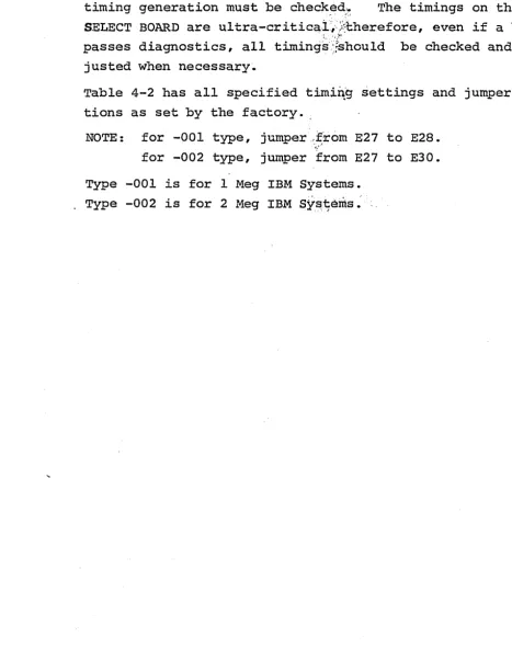
When replacing the EMM BSM SELECT PRBA, certain jumpers for timing generation must be check~d~ The timings on the BSM SELECT BOARD are ultra-critica.i/.'.i::l:herefore, even if a board passes diagnostics, all
timing{}~hould
be checked and ad-justed when necessary·.Table 4-2 has all specified timi~g settings and jumper posi-tions as set by the factory ..
NOTE: for -001 type, jumper-:~rom E27 to E28. for -002 type, jumper .from E27 to E30. Type -001 is for 1 Meg IBM Systems.
"'. • 1 '
Type -002 is for 2 Meg IBM Systems. ·
[image:56.626.69.536.178.770.2]TABLE.4-2 BSM SELECT PWBA TIMING SPECIFICATIONS
&
RECOMMENDED JUMPER POSITIONS
Refer to Assembly drawing 942905 for EMM BSM SELECT TIMING JUMPER Chart. The timing tabs are factory set and should no~ require Field Timing Changes. Refer to IBM ALD ST006 for IBM Timing Reference, and
EMM Schematic 942907, Sheet 2 for -CSX, -DOG, -SAG and -STORE Timing option should re-timing be required. The -EMM X CSX and, - EMM X STORE should be approximately as shown.
-MS ADDR SET RESET (ST373') B-A3A3Bl0
-EMM CSX AT EMM BASEPLATE {Jl0-62)
-EMM STORE AT EMM BASEPLATE {Jl0-159)
35 40
---i..._____...l..___..I
45 ~o
i
I
120 135
302 310 410 420
4-1.6
4-1. 7
4-1.8
4-1.9
BCA (Buffered controlled Address) PWBA
The EMM BCA PWBA generates the high-order address bits necessary to address (up to) 8 Megabytes of main memory. Also provided are "gated address match" (to 8 Megs) "ACB
(+ M Reg Less. Than ACB) Overide" hardware, and an "address remap/force" feature allowing full diagnostic capability. When replacing the BCA PWBA, LOC. 01AB1-T2, jumper or
switch settings, defining main memory sized, must be checked ·for validity.
Table 4-3 shows jumper or switch setting for the BCA PWBA. 4-3 BCA PNBA SWITCH SETTINGS.
Storage Protect Array PWBA
T~e EMM STOR/PROTECT ARRAY PWBA provides all k_ey storage for the system 370/148. One array card provides protect key storage _for up ~o 4 Megs of main memory. The location for the first arr~y card is 01BA4-F2. There are no jumpers or timing settings required on the STOR/PRO~ECT Array Card.
Storage Protect Data & Address PWBA
The EMM STOR/PROTECT DATA & ADDRESS board is used on all 370/148 CPU's with attached EMM 7370/148 main memory. The functions of this board are to interface the EMM STOR/PRO-TECT ARRAY PWBA to the host processor. Addresses and data
in and out are steered by the Data & Address board.
There are no timing taps to be set on the EMM Data & Address board, LOCATION 01BA4-C2.
NOTE: ALWAYS PCM'ER DOWN BOTH THE IBM 370/148, AND THE EMM
UPGRADE SUPPLY, WHEN CHANGING EMM UPGRADE CARDS.
Po~er Supply Replacement