Electron Microscopy
What Can Electron Microscopy Tell Us Beyond Crystal
Structures?
Wuzong Zhou*
[a]and Heather F. Greer
[a]Abstract: Transmission electron microscopy is a powerful tool to directly image crystal structures. Not only that, it is often used to reveal crystal size and morphology, crystal orientation, crystal defects, surface structures, superstructures, etc. However, due to the 2D nature of TEM images, it is easy to make mistakes when we try to recover a 3D structure from them. Scanning electron microscopy is able to provide information on the
parti-1. Introduction
Although electron microscopy related techniques, such as transmission electron microscopic (TEM) imaging, high resolu-tion TEM (HRTEM) imaging, selected area electron diffracresolu-tion (SAED), and energy dispersive X-ray microanalysis (EDX), can re-veal crystal structures, X-ray and neutron diffraction methods are much more accurate in determination of average crystal structures.[1]Nevertheless, electron microscopy techniques are often used to complement powder X-ray diffraction data (PXRD) to solve complex crystal structures.[2]Although collection of a
[a] School of Chemistry, University of St Andrews
St Andrews KY16 9ST, United Kingdom E-mail: [email protected]
http://www.st-andrews.ac.uk/chemistry/contact/academic/#wzhou © 2016 The Authors. Published by Wiley-VCH Verlag GmbH & Co. KGaA.·
This is an open access article under the terms of the Creative Commons Attribution License, which permits use, distribution and reproduction in any medium, provided the original work is properly cited.
Wuzong Zhou is Professor of Chemistry at the University of St Andrews. He obtained his BSc in 1982 (Fudan University) and PhD in 1988 (University of Cambridge). His interests are in solid state chemistry in general, HRTEM investigations of defects in solids and non-classical mechanisms of crystal growth.
Heather F Greer is a Research Fellow at the University of St Andrews. She received her B.Sc in Chemistry and Mathematics at the University of St Andrews in 2009, and her PhD there in 2013. Her current research interests are the electron microscopic investigation of early stage crystal growth and reversed crystal growth of various solid state materials.
cle size, morphology and surface topography. However, obtain-ing information on crystallinity of particles usobtain-ing SEM is difficult. In this microreview article, some practical cases of transmission and scanning electron microscopy investigations of inorganic crystals are reviewed. Commonly occurring uncertainties, im-perfection and misunderstandings are discussed.
PXRD pattern is easy, the data can often be difficult to interpret due to a phase problem, broadening or overlap of reflections with similar diffraction angles, especially when the structure has a large unit cell or low symmetry. Typically, in order to deter-mine a complex structure, PXRD intensity data is combined with structure factor phase information from HRTEM images,[3] rota-tion electron diffracrota-tion (RED)[4]or precession electron diffrac-tion (PED).[2,5]
common trial and error method to assess the proposed struc-tural models. For nanomaterials, on the other hand, this multi-ple scattering effect can be ignored, and the explanation of the HRTEM images is relatively simple. In many cases, determina-tion of average crystal structures of bulk materials is often not enough for us to understand the physico-chemical properties. When individual particles are examined using electron micros-copy, much more information beyond average crystal structures can be obtained, including particle size and shape, crystal ori-entation, defects, crystallinity, surface structures, superstruc-tures, etc.[8] These microstructures play important roles in ex-hibiting material properties. However, the explanations of the experimental data are not always straightforward.
In this microreview, some practical cases of electron micro-scopic investigations of inorganic crystals are discussed. Com-mon misunderstandings are explained and rectified, and the limits of the techniques are clearly delineated.
2. Crystal Size and Morphology
Among all the extra structural features detectable by electron microscopy, the easiest target is to determine crystal size and morphology. Particle size of a powder sample can be directly observed from TEM and SEM images. However, the inherent disadvantage of electron microscopy is that the number of par-ticles examined is always limited. When we have recorded a TEM/SEM image of particles, a common question for ourselves is that whether this image is typical for the sample. To convince ourselves, we normally check the sample preparation method for TEM and make sure that the particles deposited on a speci-men grid is not size selective. We also observe and record a large number of particles, at both low and high magnifications although only one or two images may be used in a final presen-tation. This will increase the likelihood of an impartial represen-tation of the sample, although this can be quite time consum-ing and expensive. When the number of measured particle sizes is large enough (say 300 to 500), the size distribution should show a smooth log-normal distribution curve.[9]
With advances in synthesis capabilities the size of nanoparti-cles is steadily decreasing and moving towards a level where nanoparticles can consist from a small, predetermined number of atoms.[10]This leaves an even greater demand for accurate nanoparticle size distribution analysis. TEM, out of all the exist-ing experimental techniques capable of measurexist-ing the particle size, is one of few techniques that allows direct (real space) visualisation of the nanoparticles. Using electron tomography, 3-dimensional images of nanoparticles can be shown. Pyrz and Buttrey[10]outlined a selection of topics which should be con-sidered to avoid over-interpretation or the improper use of the information provided in TEM micrographs in regards to particle size characterisation. The issues include magnification, analysis method (manual vs. automated) and imaging type, (bright vs. dark field) and (TEM vs. STEM). Comparison of size measure-ments of nanoparticles > 5 nm in diameter by HRTEM and an-nular dark field scanning transmission electron microscopy (ADF-STEM) have been reported to agree very well. In contrast, similar measurements for smaller particles (<2 nm) were found
to significantly differ. HRTEM has been said to overlook some particles, <2 nm in diameter, if they are amorphous or oriented off Bragg conditions.[11] It should also be noted that electron beam damage of the sample can cause modifications in the particle size, composition and/or morphology due to particle destruction/decomposition or particle coalescence.[12,13]
For nanoparticles, the crystal sizes can also be calculated from the Scherrer equation based on measuring XRD peak width at half the maximum intensity after subtraction of the background:
τ= kλ
βcosθ
whereτis the mean size of the crystalline domains,kis a shape factor, λ is the X-ray wavelength,β is the line broadening at half the maximum intensity (FWHM) in radians,θis the Bragg angle. Instrumental factors which affect peak width must be taken into account. The upper size limit for crystallite size meas-ured using the Scherrer equation is an open question but is thought to be about 100–200 nm.[14] However, particle sizes obtained from electron microscopy and the crystallite size from XRD are often in disagreement, especially those with crystallites larger than 50–60 nm or with anisotropic morphologies.[15] If the particle size is small, e.g. < 10 nm in diameter, with a narrow distribution, and all particles are highly likely to be single crys-tals, the average particle sizes measured from TEM images and calculated from XRD patterns often are in good agreement. On the other hand, the calculated size from XRD can be much smaller than that directly observed from TEM images. The main reasons are that the detected dimensions of particles using these two techniques are not along the same orientation and that the terms, “particle size” and “crystal size” are two different concepts.
If the crystals have lamellar (nanosheet, plate or belt-like), nanoneedle, nanorod or nanowire morphology, crystallite size calculated from XRD is often a good estimate for the thickness/ diameter of the crystallites but does not provide any indication of their length.[15]Revealing the dimension along the long axis of particles is much easier than observing the dimension along the short axis in TEM. For particles with anisotropic morpholo-gies such as the above, the Scherrer size should only be stated with caution and displayed with complementary microscopic imaging data. In further instances where a sample contains “large” crystals of several microns and “small” crystals, say about 150–250 nm, the calculation of crystallite size via XRD would detect the presence of the small crystals but subsequently ig-nore the larger crystals.[15]
Another explanation for discrepancies in the crystallite size values from TEM and XRD is based on a factor that the particles are probably not single crystals. They may be polycrystalline or clusters of many smaller nanocrystallites.[16]They may also be hollow crystals, or crystals containing many defects or have in-corporated organic matrix.[17,18] All types of crystal imperfec-tions would lead to extra XRD peak broadening due to micro-strain, resulting in a smaller value of crystal size.
of Mg2SiO4nanorods. Sizes of the Co particles can be directly measured from this image. However, we are unable to tell whether these particles are single crystals until HRTEM images are obtained, although according to the classical crystal growth mechanism, the Co particles should grow up with layer-by-layer deposition of Co atoms and should be single crystals at any stage. HRTEM images of Co particles with different sizes re-vealed a non-classical growth route. The Co atoms deposit on the surface of Mg2SiO4nanorods and combine into crystallites of 2 nm in diameter. These nanocrystallites do not undergo further growth, but aggregate into spherical polycrystalline clusters as shown in Figure 1 (b). Therefore, this particle has a particle size of about 30 nm in diameter as seen in the TEM image, but a crystal size of about 2 nm in diameter detectable by XRD. Only when the clusters approach to a certain size, they re-crystallize into single crystals, which often have a polyhedral shape (Figure 1, c).[19] Here we see that HRTEM images can show crystal fringes, and therefore the exact size of individual crystallites. Unfortunately the number of the crystallites exam-ined by HRTEM is typically small.
Figure 1. (a) TEM image of part of a fishbone-like particle showing lollipop-like secondary branches and sub secondary branches of Mg2SiO4with Co
particles at the ends. (b) HRTEM image of a Co particle of about 30 nm in diameter showing polycrystalline property. (c) TEM image of a Co single crys-tal, ≈ 150 nm in size, showing a polyhedral shape. [Reprinted with permission fromJ. Phys. Chem. 2004,B108, 11561–11566. Copyright (2004) American Chemical Society].
SEM is a suitable technique to show particle morphologies. However, determining morphology of particles by TEM is not straightforward, since TEM only shows two dimensional projec-ted images of three dimensional particles. For example, a cubic Co crystal could show a square shape when viewed down the <001> zone axes, or a rectangular shape along the <110> direc-tions, or a hexagonal shape along the <111> directions (Fig-ure 1, c). To reveal the actual shape of a particle, tilting the specimen grid to observe several projected images would be necessary. Determining crystal morphology using electron dif-fraction is also difficult, but not impossible, since the difdif-fraction pattern can be affected by shape factors when the crystal size is small.[20]Using XRD or neutron diffraction method to determine crystal morphology is even more difficult.
Electron tomography is often an effective method used to reconstruct the 3D structure of nanoparticles from a single axis tilt series, typically +75° to –75°, of 2D STEM or TEM images.[21]
Although this method can provide a real 3D representation of the crystal morphology, disadvantages include the difficulty to align the projections of a tomography tilt to a common axis with atomic precision and a “missing wedge” due to the inabil-ity to tilt ±90°.[22]Accuracy of the final reconstruction of the 3D volume relies on input from the number of projection images and tilt range but care should be taken to avoid electron beam damage or structural defomation during acquisition.
3. Crystal Facets and Growth Orientation
Many crystals appear as polyhedra with well defined facets. These polyhedra can be easily revealed from SEM images, which often give a 3D impression with significant image contrasts from different facets. However, to determine the crystal orienta-tions of the facets from SEM images is not always achievable, unless electron backscatter diffraction (EBSD) is performed.[23] A perfect cubic particle can only be formed with six equivalent {100} facets of a crystal with a cubic structure. But a hexagonal morphology of a crystal with a hexagonal structure can be formed with two {001} and six {100} facets or six {110} facets. SEM images cannot be used to distinguish between them.
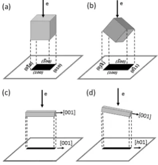
[image:3.597.59.280.310.461.2]On the other hand, if particle size is very small, it is difficult to see the particle morphology in SEM images due to a resolu-tion limit. TEM images are often used instead. However, the 2D nature of TEM images makes it difficult to recognise polyhedra. For example, a cubic Co crystallite can appear with a square shape in TEM images when the electron beam is parallel to the [001] zone axis. In this case, the observed four edges of the square particle correspond to the (100), (1
¯
00), (010) and (01¯
0) facets (Figure 2, a). SAED patterns can be used to confirm it. When the dimensions along the [100] and [010] axes are slightly different, a rectangular shape will be recorded in the TEM im-age. When viewing down the [110] direction of a cubic crystal, a rectangular shape is also observed in the TEM image as a projection of the particle. The crystal orientations of the 4 [image:3.597.344.503.515.681.2]edges can be determined by the corresponding SAED patterns and HRTEM images to be [100], [1
¯
00], [011¯
] and [01¯
1] (Figure 2, b). We can see that, in this case, the smooth edges of (011¯
) and (01¯
1) on the image of the particle do not mean there are such two facets. To understand what facets are present in TEM stud-ies, we need to tilt the crystal to reveal its 3D morphology or to use SEM images as a reference to find out whether the ob-served crystal edges in TEM images correspond to crystal fa-cets.[21]Consequently, the observed lattice fringes in a HRTEM image and the corresponding electron diffraction spots only indicate a crystal orientation which is perpendicular to the elec-tron beam. It does not have a certain relation with a crystal facet. In other words, attempting to derive crystal facets merely from observed lattice fringes in HRTEM images or diffraction spots in SAED patterns is quite risky.A similar confusion exists in TEM investigations of a crystal growth direction. Determination of the crystal growth direction is an important topic in the characterisation of low dimensional nanomaterials, and can have a large impact on understanding the physical and chemical properties of these materials.[24]For example, when nanorods or nanowires of a target material are fabricated, we wish to know what the crystal orientation is along the long axis, i.e. the prioritized growth orientation. When a nanorod with the growth direction along the [001] axis is examined in TEM, the growth direction can be determined by SAED or HRTEM imaging, subject to a correct position of the specimen.[25]Unfortunately in many studies, the growth direc-tion of individual nanorods or nanowires is based on a single electron diffraction pattern or HRTEM image, leaving some de-gree of uncertainty. If the nanorod lies down on specimen grid with its long axis perpendicular to the electron beam, the dif-fraction spots along the growth direction in the SAED pattern and the corresponding lattice fringes on the HRTEM image would show the [001] orientation (Figure 2, c). However, if the nanorod is not perpendicular to the beam, the observed crystal orientation along the long axis of the projected nanorod image would be off the [001] zone axis, say for example the [h01] axis as shown in Figure 2 (d). The real growth orientation cannot be correctly revealed. It is difficult to distinguish these two cases from a single TEM image. Zou and co-workers also discussed this problem recently.[25]Rotation of the nanorod around the axis perpendicular to both the electron beam and the long axis of the nanorod allows us to find the position with the longest projected dimension of the nanorod image, at which the ob-served crystal orientation along the long axis and the real growth orientation are parallel to each other. A correct determi-nation of the growth orientation is an important step prior to the design and growth of nanomaterials with desired orienta-tions and properties. Changes in growth direction of nanowires are well known to affect their properties.[26]
4. Local Chemical Composition
Another advantage of electron microscopy is that the chemical composition of individual particles and even small areas, span-ning several nanometers, in a particle can be analysed by EDX, since a very small beam size can be used. Variations of
composi-tion in a specimen can be examined using EDX point analysis and the elemental distribution in a particle can be shown in elemental mapping and electron energy loss spectroscopy (EELS).[27,28] For example, in a series of solid solution samples, EDX is normally used to confirm their homogeneity with differ-ent compositions.[29]It should be noted that, to determine an accurate chemical composition using EDX is not an easy job. This is because the intensity of an X-ray peak from an element is affected by many factors associated with a non-linear absorp-tion problem, such as local composiabsorp-tion, sample thickness, en-ergy of electron beam, location of the sample area examined and its surrounding environment.[30] Therefore, in practice, in addition to keeping the same experimental conditions as much as possible, many spectra, e.g. from 20 to 30 randomly selected particles, should be collected in order to reduce the systematic error. During quantification a large source of error results from the overlap of peaks from different elements. For example, ba-rium peaks overlap with titanium peaks, resulting in difficulties in the EDX analysis. The Ba Lα line appears at 4.4663 keV, whereas the TiKαline occurs at 4.5089 keV. A correct identifica-tion often relies on recognizing peaks associated with each X-ray family. Furthermore, a suitable standard specimen with a pre-determined composition close to the target samples should be used to calibrate the results. For example, monophasic BiNbO4sample was used as the standard reference for an EDX study of solid solution in the Bi2O3-Nb2O5system.[29]
Linear analysis and elemental mapping can supply informa-tion of elemental distribuinforma-tion and composiinforma-tional variainforma-tion in an examined specimen area.[31]For example, in a synthesized STA-7 zeolite sample, EDX point analysis indicated that the Si/Al ratio varies against the distance from the center to the edge of the crystals.[32]For some core-shell structures, the core and shell may have a similar structure and the HRTEM image contrast is not high, making it difficult to distinguish them. EDX elemental mapping, on the other hand, can show clearly the separation of compositions between the core and the shell in a nanometer scale.[27,33]In these studies, the accuracy of the chemical com-position would not be high, but the inhomogeneous distribu-tion of elements is obvious.
Elemental analysis using STEM has a tremendous advantage. STEM significantly reduces the interaction between the electron beam and the sample, therefore greatly reduces sample dam-age. It is noted that the recently developed state-of-the-art EDX system in a Cs corrected STEM can present elemental mapping at atomic resolution. However, the data can only be interpreted qualitatively because the elastic and thermal scattering of the electron probe confounds quantitative analysis.[34]High resolu-tion elemental mapping can be collected with sample tilting to create a three dimensional re-construction. This method is particularly useful for particles with a domain structure, or core-shell structure, or any phase separation.
5. Surface Profile Imaging
nano-thick layers in crystals, when HRTEM surface profile im-ages are observed.[35]HRTEM surface profile imaging is comple-mentary to the standard surface science techniques such as scanning tunnelling microscopy (STM), atomic force microscopy (AFM), etc. The major difference is that STM and AFM show 2D images of the top surface layer, while HRTEM only shows 1D images of the top surface layer, i.e. a profile view.[36]However, this characteristic engenders an advantage of HRTEM: not only can the top surface be observed, but also the crystal structures underneath the surface can be imaged.[37]If the surface has a different crystalline phase, the thickness of this layer and its intergrowth with the core crystal can be revealed. For example, the (001) surface of La2CuO4 often terminates with several atomic layers of La2O3.[38]Regarding physico-chemical proper-ties of inorganic solids, surface layers with nanometer scaled thickness is probably more important than only a top atomic layer. This advantage also makes HRTEM a suitable tool to inves-tigate crystals with an amorphous surface coating layer.[39]
The amorphous layer on a crystal surface observed in HRTEM images could be due to decomposition of the parent crystal or deposition of amorphous carbon or other contaminates. The latter could form during synthesis or be deposited under elec-tron beam irradiation. When both decomposed crystal and de-posited amorphous carbon are present on crystal surface, their different image contrasts allow us to easily recognise them. The inner layer is normally the decomposed layer and the outer layer is contaminate. If there is only one amorphous layer, it is often difficult to determine whether it is decomposed crystal or deposited carbon. Making a conclusion without further testing would be inappropriate. An experienced operator would per-form one or more experiments to discover the nature of a sur-face amorphous layer, if it is necessary.
First, if the coating layer is thick, e.g. a few nanomaters, using a narrow beam, the local chemical composition of the coating layer can be detected. A good example was demonstrated by EDX point analysis of an amorphous surface layer of Hg-con-taining high Tc superconducting cuprate. It was found that the surface of HgBa2CuO4crystals often decomposed into an amor-phous layer and lost Hg simultaneously.[40] Secondly, if an amorphous carbon layer formed during electron beam irradia-tion, its thickness may increase on extending the exposure time of electron beam as the hydrocarbon molecules are polymer-ised by the incoming (or outgoing) electrons.[13]
If the surface layer is decomposed crystal with the same composition as that of the parent crystal, it may recrystallize into the parent crystal under electron beam annealing. A clean crystal surface may be achieved as shown in HRTEM surface profile images of YBa2Cu3O7.[41] Under electron beam irradia-tion, re-crystallisation started at the interface between the crys-tal and the amorphous layer, and extended across the whole amorphous layer. Finally, a clean surface is created (Figure 3). this work indicated that the decomposed surface of this speci-men can be repaired by thermal annealing and can actually help to improve the quality of the superconducting property of the material. The decomposed layer on the surface of HgBa2CuO4 suffers a great loss of Hg, and therefore can only re-crystallise into barium copper oxide, which has a close
rela-Figure 3. HRTEM surface profile images of YBa2Cu3O7viewed down the [110]
direction. Top: the initial image showing a thin layer of disordered coating. Bottom: an image of the same area after electron beam irradiation for 3 hours. Clean (113), (110) and (112) surfaces are indicated. [Reprinted with permission fromJ. Solid State Chem.1992,98, 437–441. Copyright (1992) Elsevier Inc.].
tion in structure with HgBa2CuO4, and therefore, can intergrow with the parent crystal very well.[42]
Another example is that by Cölfen and co-workers[43]when they reported for the first time, a 3 to 5 nm thick continuous layer of amorphous calcium carbonate (ACC) on the surface of crystalline aragonite platelets in nacre of haliotis laevigata, a species of sea snail. Under intense electron irradiation, HRTEM images showed the ACC layer began to crystallise, forming sev-eral crystalline nuclei of aragonite that was slightly distorted compared with the core of the aragonite platelet.
6. Superstructures
Many superstructures in inorganic crystals occur due to order-ing of lattice distortion or light elements. The scatterorder-ing factor of electron diffraction, fB, is very roughly proportional to Z1/3 (Z: atomic number), while this order for X-ray scattering factor is about 1. This means that the scattering of electrons is less sensitive to atomic number. In other words, electron diffraction is a better method than XRD in detecting light elements, e.g. oxygen in metal oxides and, therefore, superstructures based on oxygen ordering.[7,44]In many cases, long-range ordering in complex solids such as LiNi0.5Mn0.5O2 discovered by electron diffraction would be extremely difficult, if not impossible to de-tect by powder XRD and neutron diffraction.[45]
[image:5.597.318.536.69.270.2]When the positions of the diffraction spots were measured carefully, it was found that many superstructures in solid solu-tions were incommensurate.[47]Figure 4 shows some SAED pat-terns from some solid solution materials in the Bi-W-Nb-O mixed oxide system, along the [11
¯
0] zone axis of the fluorite subunit cell. The first impression might be that a threefold su-perstructure exists in these solids. A careful measurement, how-ever, reveals that a true threefold superstructure only presents in Bi10W2O21. In the other three SAED patterns, the two satellite diffraction spots due to the superlattice are not at the 1/3 and 2/3 positions in between (000) and (111) spots. An incommen-surate structure can be regarded as a partially ordered struc-ture, although unearthing a unit cell in a long range is impossi-ble. On the other hand, to investigate the nature of the order-ing, we can still focus on a small area in HRTEM images, from which a hypothetical commensurate super unit cell can be de-rived as a reasonable approach.[29]Figure 4. SAED spots along the [11¯0] direction of the fluorite-like subcell of some solid solution oxides in the Bi-W-Nb-O system, with compositions of (a) Bi8Nb2O17, (b) Bi17WNb3O36, (c) Bi17W2Nb3O39, and (d) Bi10W2O21. The relative
positions of the superstructure diffraction spots are indicated. [Reprinted with permission fromJ. Solid State Chem.2002,163, 479–483. Copyright (2002) Elsevier Science (USA)].
There is another reason to have extra weak diffraction spots in SAED patterns. Some systematically absent diffraction spots appear, which do not change the unit cell, but seem to reduce the symmetry of the structure. Possible multiple scattering ef-fect should be considered. If this is the case, these extra diffrac-tion peaks should not be observed in the corresponding XRD pattern, since no multiple scattering takes place in XRD. When the same SAED pattern is recorded at several areas with differ-ent specimen thickness, the relative intensities of these extra spots would be significantly changed. Specimen tilting would also notably change the relative intensities of the extra spots.
7. Defects
Investigation of defects in solids using electron microscopy is a common and important research field. The defects, including point defects, layered defects, twin defects, anti-phase defects, stacking faults, domain structures, dislocations[48]etc., can
sig-nificantly affect the properties of the materials. In this article, electron microscopic images of some not obvious or hidden defects are discussed.
7.1. Twin and anti-Phase Defects
Both twin defects and anti-phase defects have a planar bound-ary and have two domains with identical crystal structures. When viewing down a direction parallel to an anti-phase boundary plane and perpendicular to the vector of phase shift-ing, the HRTEM image would show a dark contrast line on the boundary and, on the two sides of the boundary, the lattice patterns would shift to each other by a dimension of half a unit cell.[49]The dark image contrast is mainly contributed from diffraction contrast. In low magnification TEM images, no lattice fringes can be observed, but the image contrast of the anti-phase boundary is higher. This contrast can be even further enhanced by using a smaller objective aperture.
In the case of a twin defect, a dark line on the twin boundary can also be observed when the electron beam is parallel to the twin plane. The lattice patterns on both sides have mirror symmetry with the principal crystal orientation which bends to an angle smaller than 180°. Figure 5(a) shows a HRTEM image of a Si nanowire containing two twin defects, when viewed down the [111
¯
] zone axis. When the nanowire was rotated around the long axis of the nanowire by a small angle (e.g. 15°), the mirror symmetric lattice patterns disappeared and the fine dark lines of the twin planes became less obvious. A more fasci-nating change is that the lattice fringes may extend across the twin boundaries (Figure 5, b). This experiment tells us that a 2D planar defect boundary can unquestionably only be observed when viewing down the correct direction. A HRTEM image like that in Figure 5(b) does not mean it is defect free. The twin planes are actually hidden at the positions of wide dark belt-shaped regions, resulting from a projection of the twin planes with a tilted angle.[50]For the same reason, in a profile HRTEM image of a cyclic twinning nanowire containing five twin planes in a fivefold symmetry, no more than one twin plane can be observed at the same time.[20]Figure 5. (a) HRTEM image of a Si nanowire with two twin defects. (b) HRTEM image of the same nanowire after rotating about 15° around the [112] axis. The straight line indicates the lattice fringes extend across the original twin defect planes. [Reproduced from ref. [50] with permission from The Royal Society of Chemistry].
7.2. Point Defects
[image:6.597.326.526.527.630.2]and 1D linear defects, rotation of the specimen has limited ef-fect on the image contrast patterns of 0D point deef-fects. For example, a spherical inclusion in a crystal would have identical TEM contrast pattern viewed down along any direction.[52] Spherically symmetrical coherency strains resulting from spheri-cal domains lead to a butterfly-like pattern mainly contributed by diffraction contrast. When the spherical domain size reduces, the dark circle image contrast becomes smaller. The smallest point defects in crystals are probably excess atoms in interstitial sites or vacancies at crystal sites. Metal oxides with nonstoichio-metric oxygen are in great demand as their ionic conductivity can be improved by controlling the excess oxygen anions or vacancies.[53]
Imaging of point defects by TEM is often very challenging and is not suitable to provide a quantitative measure of the point defect concentration and structure. Firstly, TEM relies on diffraction and interference effect and is therefore not very sen-sitive to randomly distributed point defects. Frequently, point defects can only be detected by HRTEM when they are in clus-ters or columns. Secondly, almost all TEM samples are many unit cells thick, and the contrast generated from point defects can often be blocked by the signal from the normal lattice above and below the defect.[54]However, in some special cases, very small point defects, such as random excess oxygen anions, can be detected. Figure 6 (a) shows a typical HRTEM image of La4Sr8Ti12O38in a perovskite structure with excess oxygen, with which a high anion conductivity was achieved.[55]Since there is not a large enough space for guest atoms in a perfect perov-skite crystal with a formula of ABO3, the excess oxygen atoms must go to interstitial sites and build up local lattice strain. The resolution of the electron microscope (JEOL JEM-2010) used is not high enough to image randomly located individual oxygen atoms. However, these oxygen atoms would cause local lattice distortion within several atomic layers, leading to a formation of dark spots in the image due to diffraction contrast. The inset of Figure 6 (a) is an enlarged image of one such spot, on which lattice distortion can be seen. As a comparison, Figure 6 (b) shows a HRTEM image of Mg2SiO4 nanorod with Co clusters deposited on its surface. Randomly distributed dark spots are also visible but no local lattice distortion is observed.[19]Excess
Figure 6. (a) HRTEM image of La4Sr8Ti12O38, viewing down the [100] zone
axis.[55]The arrows indicate some dark spots, which are the locations of
ex-cess oxygen anions. The inset shows an enlarged image of a dark spot. (b) HRTEM image of Mg2SiO4nanorod containing Co clusters on its surface.[19]
[(a) Reproduced from Ref. 55 with permission from Nature Publishing Group (2006); (b) Reprinted with permission fromJ. Phys. Chem. Ser. B2004,108, 11561–11566. Copyright (2004) American Chemical Society].
oxygen anions embedded in silicate apatite were also im-aged.[56]
7.3. Disordered Core in Single Crystal Shell
SEM allows us to view particle morphologies. Figure 7(a) shows a SEM image of a perfect icositetrahedral particle of synthetic zeolite analcime. According to the classical theory of crystal growth, the so-called Bravais–Friedel–Donnay–Harker (BFDH) law,[57]crystals exhibit a high symmetric polyhedral shape with facets achieved by different growth rates along different crystal orientations. In other words, the surfaces with the lowest growth rate will be maintained as the final crystals facets. Dur-ing this “bottom-up” growth process, particles at any stage should be single crystals. However, making a conclusion of a single crystal merely based on the SEM images, e.g. that in Fig-ure 7 (a), is quite risky. In fact, when single crystal XRD was performed on a perfect icositetrahedral particle, the resulted pattern showed a strong polycrystalline ring in addition to some sharp diffraction spots.[58]
Figure 7. (a) SEM image of an icositetrahedral particle of zeolite analcime. (b) SEM image of a similar icositetrahedron of zeolite analcime with a broken area, showing a polycrystalline core. (c) TEM image of a particle of zeolite A with corresponding SAED pattern. (d) TEM image of the same particle after electron beam irradiation for a few minutes. The inset is the corresponding SAED pattern.[61] [(a,b)Reprinted with permission from J. Am. Chem. Soc.
[image:7.597.324.525.310.484.2] [image:7.597.70.269.562.669.2]Since then, this phenomenon has been observed in many other materials, including zeolite A, CaTiO3 perovskite, ZnO, CuPt alloy, metal-organic frameworks, and even organic crys-tals.[59–61]
Figure 7 (c) is a TEM image of a zeolite A particle with the corresponding SAED pattern viewed from the [001] projection. Both the regular shape and the diffraction pattern are normal and indicate a single crystal state. However, under electron beam irradiation for a few minutes, a core-shell structure was detected, i.e. an amorphous core in a very thin single crystal shell (Figure 7, d).[61]Under electron beam exposure, it was seen that the core material appeared more disordered, with a mobile fluid-like appearance and had separated from the thin shell. The almost identical SAED pattern in Figure 7 (d) was actually from the shell of 7 nm in thickness. Consequently, a single crystal type SAED pattern does not always mean the particle under examination is single crystal. On an opposite note, data used to assign CaCO3mesocrystals, which are a 3D array of iso-oriented single crystal particles are commonly misinterpreted.[18] Rough-ness on the calcite/polymer crystal surface can be falsely inter-preted as homogeneous nanoparticle substructure when in fact, these nanoparticles are only present as a thin surface layer. SEM/TEM investigations of the non-classical reversed crystal growth allow us to observe many unusual phenomena. For ex-ample, HRTEM images show that, at an early stage of the growth of zeolite analcime, the shape of nanocrystallites is plate-like with the short axes along the [111] direction, instead of an icositetrahedron or cube. These nano-crystallites aggre-gated into some large disks with a perfect self-orientation. Therefore, SAED patterns from these polycrystalline disks are single crystal-like.[58] During the growth of metal organic framework, MOF-5, the first crystalline particles are Zn5(OH)8(NO3)2·2H2O nanoplatelets with a diameter of 5– 10 nm. These nanoplatelets aggregate with the assistance of surface adsorbed 1,4-BDC molecules to form large microplates. Zn5(OH)8(NO3)2·2H2O underwent a phase transformation to MOF-5. Therefore, in this system, nucleation of MOF-5 crystals does not take place in the solution, but in soft matter aggre-gates.[60]Because a single crystal shell forms first in a reversed crystal growth route, mass transportation between the particle cores and the outside environment becomes difficult. If the dis-ordered core has a lower density than the crystal, the final crys-tals would have a hole in the middle. Therefore, the reversed crystal growth mechanism can describe the formation of many hollow crystals.
8. Summary and Outlook
Although HRTEM plays an important role in determination of some complex crystal structures, most researches of electron microscopy, including SEM and TEM, are focussed on micro-structures beyond crystal micro-structures, such as crystal size and morphology, crystal facets and growth orientation, local com-position and elemental distribution, surface structures and su-perstructures, and various defects. All of these can be regarded as local structures and the information of these microstructures from XRD and neutron diffraction methods is very limited.
How-ever, being deceived by the direct imaging of specimens and their crystal structures, some researchers would simply over-interpret the electron microscopic data. We sometimes see “a real image leads to a wrong conclusion”. This article, using some examples, shows how to avoid the over-interpretation of SEM and TEM results. For example, we should not be confused by “particle size” and “crystal size”; extra care should be taken when we try to reveal particle morphology from TEM images; a particle with a perfect polyhedral shape does not mean it must be a single crystal, etc.
Unlike optical microscopy, the formation of image contrast in SEM and TEM is very complicated. For example, in TEM in-cluding HRTEM, the formation of image contrast patterns can obey three different principal mechanisms due to different magnification and other microscopic conditions, i.e. mass-thick-ness contrast, diffraction contrast, and phase contrast. The other electron microscopy related techniques, such as scanning trans-mission electron microscopic (STEM) imaging, high-angle annu-lar dark-field imaging (HAADF) bring in new elements to the formation mechanisms of image contrast. To correctly under-stand the images, we must know the principles of these tech-niques.
Using focused ion beam (FIB) and 3D reconstruction tech-nique, the inner structures of crystals can be easily revealed. Consequently, for studying non-classical crystal growth, more detailed core-shell structures, early stage crystal growth in soft matter aggregates, can be observed. This will help us to under-stand the non-classical crystal growth, and therefore further control crystal size and morphology.
The state-of-the-art Cs-corrected STEM has a much smaller beam probe and much higher sensitivity to the surface proper-ties of specimens. Detecting nanoscale dipole field and mag-netic field in crystalline samples becomes possible. These fields play important roles in crystal growth and self-assembly. Inves-tigation of this is a new direction of electron microscopy. At any stage, it is important to know exactly what we can achieve from the electron microscopic results.
Acknowledgments
W. Z. thanks Professor Jun Yuan for a useful discussion during the revision of this article. The authors wish to thank Engineer-ing and Physical Sciences Research Council (EPSRC) for financial support to the electron microscopy facility (EP/F019580/1) and for a Platform Grant (EP/K015540/1).
Keywords: Electron microscopy · Electron diffraction · Crystal growth · Solid-state structures · Nanostructures
[1] a) Z. Sofer, P. Šimek, O. Jankovský, D. Sedmidubský, P. Beran, M. Pumera, Nanoscale2014,6, 13082–13089; b) C. C. Wilson,Single Crystal Neutron Diffraction from Molecular Materials,2000, World Scientific, Singapore. [2] a) L. B. McCusker, C. Baerlocher,Chem. Commun.2009, 1439–1451; b) F.
[4] a) P. Guo, J. Shin, A. G. Greenaway, J. G. Min, J. Su, H. J. Choi, L. Liu, P. A. Cox, S. B. Hong, P. A. Wright, X. Zou,Nature2015,524, 74–78; b) J. Su, E. Kapaca, L. Liu, V. Georgieva, W. Wan, J. Sun, V. Valtchev, S. Hovmöller, X. Zou,Microporous Mesoporous Mater.2014,189, 115–125.
[5] a) E. Mugnaioli, T. Gorelik, U. Kolb,Ultramicroscopy2009,109, 758–765; b) J. Gjønnes, V. Hansen, A. Kverneland,Microsc. Microanal.2004,10, 16– 20.
[6] a) B. D. Forbes, L. Houben, J. Mayer, R. E. Dunin-Borkowski, L. J. Allen, Ultramicroscopy2014,147, 98–105; b) C. Huang, S. Wu, A. M. Sanchez, J. J. P. Peters, R. Beanland, J. S. Ross, P. Rivera, W. Yao, D. H. Cobden, X. Xu,Nat. Mater.2014,13, 1096–1101; c) H. Rösner, C. Kübel, Y. Ivanisenko, L. Kurmanaeva, S. V. Divinski, M. Peterlechner, G. Wilde,Acta Mater.2011, 59, 7380–7387.
[7] a) J. M. Thomas, P. A. Midgley, C. Ducati, R. K. Leary,Prog. Nat. Sci. Mater. Int.2013,23, 222–234; b) X. Xie, W. Shen,Nanoscale2009,1, 50–60; c) J. S. Chen, T. Zhu, Q. H. Hu, J. Gao, F. Su, S. Z. Qiao, X. W. Lou,ACS Appl. Mater. Interfaces2010,2, 3628–3635.
[8] a) X. Zhang, J. Qin, Y. Xue, P. Yu, B. Zhang, L. Wang, R. Liu,Sci. Rep.2014, 4, 4596; b) J. Zhang, F. Shi, J. Lin, D. Chen, J. Gao, Z. Huang, X. Ding, C. Tang,Chem. Mater.2008,20, 2937–2941; c) P.-C. Lin, S. Lin, P. C. Wang, R. Sridhar,Biotechnol. Adv.2014,32, 711–726.
[9] a) R. Raja, V. B. Golovko, J. M. Thomas, A. Berenguer-Murcia, W. Z. Zhou, S. H. Xie, B. F. G. Johnson,Chem. Commun.2005, 2026–2028; b) C. Zhang, S. Y. Hwang, Z. Peng,J. Mater. Chem. A2014,2, 19778–19787; c) P. Zhang, Y. Gong, H. Li, Z. Chen, Y. Wang,Nat. Commun.2013,4, 1593–1603; d) Y. Holade, N. E. Sahin, K. Servat, T. W. Napporn, K. B. Kokoh,Catalysts
2015,5, 310–348.
[10] W. D. Pyrz, D. J. Buttrey,Langmuir2008,24, 11350–11360. [11] T. Walther,J. Microsc.2015,257, 171–178.
[12] R. F. Egerton, P. Li, M. Malac,Micron2004,35, 399–409.
[13] a) G. Shi, S. Bao, W. Lai, Z. Rao, X. Zhang, Z. Wang,Scanning2013,35, 69–74; b) J. M. Yuk, M. Jeong, S. Y. Kim, H. K. Seo, J. Kim, J. Y. Lee,Chem. Commun.2013,49, 11479–11481.
[14] a) A. Weibel, R. Bouchet, F. Boulc'h, P. Knauth,Chem. Mater.2005,17, 2378–2385; b) A. Barroso-Bogeat, M. Alexandre-Franco, C. Fernández-González, V. Gómez-Serrano,J. Microsc.,2015, DOI: 10.1111/jmi.12323. [15] V. Uvarov, I. Popov,Mater. Charact.2013,85, 111–123.
[16] S. Pabisch, B. Feichtenschlager, G. Kickelbick, H. Peterlik,Chem. Phys. Lett.
2012,521, 91–97.
[17] a) T. Ungár,Scr. Mater.2004,51, 777–781; b) B. Pokroy, A. N. Fitch, E. Zolotoyabko,Adv. Mater.2006,18, 2363–2368.
[18] Y.-Y. Kim, A. S. Schenk, J. Ihil, A. N. Kulak, N. B. J. Hetherington, C. C. Tang, W. W. Schmahl, E. Griesshaber, G. Hyett, F. C. Meldrum,Nat. Commun.
2014,5, 4341.
[19] S. H. Xie, W. Z. Zhou, Y. Q. Zhu,J. Phys. Chem. B2004,108, 11561–11566. [20] X. Fu, J. Yuan,Nanoscale2013,5, 9067–9072.
[21] a) X. Xu, Z. Saghi, R. Gay, G. Möbus,Nanotechnology2007,18, 225501; b) I. Florea, C. Feral-Martin, J. Majimel, D. Ihiawakrim, C. Hirlimann, O. Ersen,Cryst. Growth Des.2013,13, 1110–1121; c) L. Cervera Gontard, R. E. Dunin-Borkowski, D. Ozkaya,J. Microsc.2008,232, 248–259. [22] a) M. C. Scott, C.-C. Chen, M. Mecklenburg, C. Zhu, R. Xu, P. Ercius, U.
Dahmen, B. C. Regan, J. Miao,Nature2012,483, 444–448; b) B. Zhang, D. S. Su,Angew. Chem. Int. Ed.2013,52, 8504–8506;Angew. Chem.2013, 125, 8662–8664; c) B. Goris, A. De Backer, S. Van Aert, S. Gómez-Graña, L. M. Liz-Marzán, G. Van Tendeloo, S. Bals,Nano Lett. 2013,13, 4236– 4241.
[23] V. Randle,J. Microsc.1999,195, 226–232.
[24] a) S. A. Fortuna, X. Li,Semicond. Sci. Technol.2010,25, 024005; b) T. R. Kuykendall, M. V. P. Altoe, D. F. Ogletree, S. Aloni,Nano Lett.2014,14, 6767–6773.
[25] Z. Zhang, X. Han, J. Zou,Sci. China Mater.2015,58, 433–440.
[26] a) T. Kuykendall, P. J. Pauzauskie, Y. Zhang, J. Goldberger, D. Sirbuly, J. Denlinger, P. Yang,Nat. Mater.2004,3, 524–528; b) A. H. Chin, T. S. Ahn, H. Li, S. Vaddiraju, C. J. Bardeen, C.-Z. Ning, M. K. Sunkara,Nano Lett.
2007,7, 626–631.
[27] S. Ristig, O. Prymak, K. Loza, M. Gocyla, W. Meyer-Zaika, M. Heggen, D. Raabe, M. Epple,J. Mater. Chem. B2015,3, 4654–4662.
[28] a) L. Gan, M. Heggen, S. Rudi, P. Strasser,Nano Lett.2012,12, 5423–5430; b) J.-H. Lee, J.-T. Jang, J.-S. Choi, S. H. Moon, S.-H. Noh, J.-W. Kim, J.-G. Kim, I.-S. Kim, K. I. Park, J. Cheon,Nat. Nanotechnol.2011,6, 418–422.
[29] W. Z. Zhou, D. A. Jefferson, J. M. Thomas,Proc. Roy. Soc. Lond. Ser. A1986, 406, 173–182.
[30] R. Johnson,Energy dispersive X-ray microanalysis, Noran Instruments, Mid-dleton, Wisconsin,1999.
[31] F. Mou, L. Xu, H. Ma, J. Guan, D.-R. Chen, S. Wang,Nanoscale2012,4, 4650–5657.
[32] D. Tzoulaki, L. Heinke, M. Castro, P. Cubillas, M. W. Anderson, W. Z. Zhou, P. A. Wright, J. Kärger,J. Am. Chem. Soc.2010,132, 11665–11670. [33] J. Park, M. D. Porter, M. C. Granger,Langmuir2015,31, 3537–3545. [34] G. Kothleitner, M. J. Neish, N. R. Lugg, S. D. Findlay, W. Grogger, F. Hofer,
L. J. Allen,Phys. Rev. Lett.2014,112, 085501.
[35] a) F. Maier-Flaig, C. Kübel, J. Rinck, T. Bocksrocker, T. Scherer, R. Prang, A. K. Powell, G. A. Ozin, U. Lemmer,Nano Lett.2013,13, 3539–3545; b) L. Han, U. Wiedwald, J. Biskupek, K. Fauth, U. Kaiser, P. Ziemann,Beilstein J. Nanotechnol.2011,2, 473–485; c) Y. C. Bae, A. R. Lee, G. H. Baek, J. B. Chung, T. Y. Kim, J. G. Park, J. P. Hong,Sci. Rep.2015,5, 13362. [36] A. N. Chiaramonti, L. D. Marks,J. Mater. Res.2005,20, 1619–1627. [37] a) P.-X. Gao, P. Shimpi, H. Gao, C. Liu, Y. Guo, W. Cai, K.-T. Liao, G. Wrobel,
Z. Zhang, Z. Ren, H.-J. Lin,Int. J. Mol. Sci.2012,13, 7393–7423; b) X. Zou, H. Fan, Y. Tian, S. Yan,CrystEngComm2014,16, 1149–1156; c) X. Huang, M.-G. Willinger, H. Fan, Z.-L. Xie, L. Wang, A. Klein-Hoffmann, F. Girgsdies, C.-S. Lee, X.-M. Meng,Nanoscale2014,6, 8787–8795.
[38] W. Z. Zhou, D. A. Jefferson, W. Y. Liang,Surf. Sci.1989,209, 444–454. [39] a) C. Lai, Q. Wu, J. Chen, L. Wen, S. Ren,Nanotechnology 2010, 21,
215602; b) F. Li, P. D. Nellist, D. J. H. Cockayne,Appl. Phys. Lett.2009,94, 263111.
[40] W. Z. Zhou, A. Asab, I. Gameson, D. A. Jefferson, P. P. Edwards,Phys. C
1995,248,1–10.
[41] W. Z. Zhou, D. A. Jefferson, W. Y. Liang,J. Solid State Chem.1992,98, 437–441.
[42] W. Z. Zhou, J. M. Thomas,Curr. Opin. Solid State Mater. Sci.2001,5, 75– 83.
[43] N. Nassif, N. Pinna, N. Gehrke, M. Antonietti, C. Jäger, H. Cölfen,Proc. Natl. Acad. Sci. USA2005,102, 12653–12655.
[44] V. Pecharsky, P. Zavalij,Fundamentals of powder diffraction and structural characterisation of materials, Springer, New York,2009.
[45] Y. S. Meng, G. Ceder, C. P. Grey, W.-S. Yoon, Y. Shao-Horn,Electrochem. Solid-State Lett.2004,7, A155–A158.
[46] a) W. Z. Zhou,J. Solid State Chem.1992,101, 1–17; b) W. Z. Zhou, D. A. Jefferson, J. M. Thomas,J. Solid State Chem.1987,70, 129–136; c) W. Z. Zhou,J. Solid State Chem.1988,76, 290–300.
[47] W. Z. Zhou,J. Solid State Chem.2002,163, 479–483.
[48] a) U. Wiedwald, L. Han, J. Biskupek, U. Kaiser, P. Ziemann,Beilstein J. Nanotechnol.2010,1, 24–47; b) F. Meng, M. Estruga, A. Forticaux, S. A. Morin, Q. Wu, Z. Hu, S. Jin,ACS Nano2013,7, 11369–11378; c) H. Shi, B. Dong, W. Wang,Nanoscale2012,4, 6389–6392; d) J. C. Meyer, C. Kisie-lowski, R. Erni, M. D. Rossell, M. F. Crommie, A. Zettl,Nano Lett.2008,8, 3582–3586; e) K. P. McKenna, F. Hofer, D. Gilks, V. K. Lazarov, C. Chen, Z. Wang, Y. Ikuhara,Nat. Commun.2014,5, 5740–5747; f ) M. I. den Hertog, C. Cayron, P. Gentile, F. Dhalluin, F. Oehler, T. Baron, J. L. Rouviere, Nano-technology2012,23, 025701.
[49] A. C. McLaughlin, W. Z. Zhou, J. P. Attfield, A. N. Fitch, J. L. Tallon,Phys. Rev. B1999,60, 7512–7516.
[50] Z. X. Su, C. Dickinson, Y. T. Wan, Z. L. Wang, Y. W. Wang, J. Sha, W. Z. Zhou,CrystEngComm2010,12, 2793–2798.
[51] P. A. Wright, W. Z. Zhou, J. Pérez-Pariente, M. Arranz,J. Am. Chem. Soc.
2005,127, 494–495.
[52] M. F. Ashby, L. M. Brown,Philos. Mag.1963,8, 1649–1676. [53] G. Wang, Y. Ling, Y. Li,Nanoscale2012,4, 6682–6691.
[54] a) C. A. Geiger,Solid solutions in silicate and oxide systems, Eötvös Univer-sity Press, Budapest, Hungary,2001; b) G. Van Tendeloo, D. Van Dyke, S. J. Pennycook,Handbook of nanoscopy, Wiley-VCH, Weinheim, Germany,
2012.
[55] J. C. Ruiz-Morales, J. Canales-Vázquez, C. Savaniu, D. Marrero-López, W. Z. Zhou, J. T. S. Irvine,Nature2006,439, 568–571.
[56] Y. Q. Zhang, Z. X. Su, A. K. Azad, W. Z. Zhou, J. T. S. Irvine,Adv. Energy Mater.2012,2, 316–321.
Donnay, D. Harker,Am. Mineral.1937,22, 446–467; d) P. Hartman, W. G. Perdok,Acta Crystallogr.1955,8, 521–524.
[58] X. Y. Chen, M. H. Qiao, S. H. Xie, K. N. Fan, W. Z. Zhou, H. Y. He,J. Am. Chem. Soc.2007,129, 13305–13312.
[59] a) X. F. Yang, J. X. Fu, C. J. Jin, J. Chen, C. L. Liang, M. M. Wu, W. Z. Zhou, J. Am. Chem. Soc.2010,132, 14279–14287; b) K. Self, H. J. Zhou, H. F. Greer, Z. R. Tian, W. Z. Zhou,Chem. Commun.2013,49, 5411–5413; c) F. J. Yu, W. Z. Zhou,Prog. Nat. Sci. Mater. Int.2013,23, 331–337; d) J. R. G. Sander, D.-K. Bučar, J. Baltrusaitis, L. R. MacGillivray,J. Am. Chem. Soc.
2012,134, 6900–6903; e) K. Self, M. Telfer, H. F. Greer, W. Z. Zhou,Chem. Eur. J.2015,21, 19090–19095.
[60] C. M. Zheng, H. F. Greer, C.-Y. Chiang, W. Z. Zhou,CrystEngComm2014, 16, 1064–1070.
[61] J. F. Yao, D. Li, X. Y. Zhang, C. H. Kong, W. B. Yue, W. Z. Zhou, H. T. Wang, Angew. Chem. Int. Ed.2008,47, 8397–8399;Angew. Chem.2008,120, 8525–8527.
Electron Microscopy Some examples of conventional SEM and TEM studies of inorganic crystals
W. Zhou,* H. F. Greer ... 1–11
are reviewed. Typical problems of mis-What Can Electron Microscopy Tell interpretation of the images are
dis-Us Beyond Crystal Structures? cussed.
![Figure 3. HRTEM surface profile images of YBa2Cu3O7 viewed down the [110]direction. Top: the initial image showing a thin layer of disordered coating.Bottom: an image of the same area after electron beam irradiation for 3hours](https://thumb-us.123doks.com/thumbv2/123dok_us/8982212.393872/5.597.318.536.69.270/figure-surface-profile-direction-initial-disordered-electron-irradiation.webp)
![Figure 5. (a) HRTEM image of a Si nanowire with two twin defects. (b) HRTEMimage of the same nanowire after rotating about 15° around the [112] axis.The straight line indicates the lattice fringes extend across the original twindefect planes](https://thumb-us.123doks.com/thumbv2/123dok_us/8982212.393872/6.597.106.234.272.457/nanowire-hrtemimage-nanowire-rotating-straight-indicates-original-twindefect.webp)

