Interfacial Reactions Between Sn 58 mass%Bi Eutectic Solder and (Cu, Electroless Ni P/Cu) Substrate
6
0
0
Full text
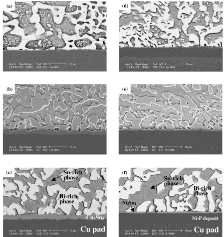
(2) 1822. J.-W. Yoon, C.-B. Lee and S.-B. Jung. Fig. 1 SEM micrographs of the interface between Sn–58Bi solder and Cu substrate (a)-(c), Sn–58Bi solder and electroless Ni–P/Cu substrate (d)-(f): as-soldered (a), (d) and after aging at 100◦ C for 30days (b), (e) and 60days (c), (f).. ysis software. 3. Results and Discussion Figure 1 shows the SEM micrographs of intermetallic compound layers for the interface between Sn–58Bi solder and (Cu, electroless Ni–P/Cu) substrate aged at 100◦ C for different aging times. In the as-soldered joints, the layer thickness of the Cu6 Sn5 and Ni3 Sn4 intermetallic compound were approximately 0.45 and 0.12 µm, respectively. EDX analysis of the intermetallic compounds indicated that their compositions were close to those of the Cu6 Sn5 and Ni3 Sn4 phases. The interface between the Cu6 Sn5 and solder displays a scalloped morphology as shown in Figs. 1(a)–(c). As evident from the Figs. 1(d)–(f), Ni3 Sn4 intermetallic compound exhibited the layered structure, and its thickness increased rather slowly. with aging time, reaching only 1.12 µm for 60 days of aging at 100◦ C. Figure 2 shows the SEM micrographs of the interface between Sn–58Bi solder and (Cu, electroless Ni–P/Cu) substrate aged at 120◦ C for 50 days. The aged Sn–58Bi/Cu joint consists of the Cu substrate, the Cu6 Sn5 intermetallic compound layer, the Bi-rich phase and the Sn-rich phase. On the other hand, the aged Sn–58Bi/electroless Ni–P joint consists of the Cu substrate, the Ni–P deposits, the Ni3 Sn4 intermetallic compound layer, the Bi-rich phase and the Sn-rich phase. The Bi-rich and Sn-rich phases exhibited extensive coarsening due to isothermal aging. Especially, the growth of the intermetallic compound layers depleted the Sn-rich phase adjacent to the Cu6 Sn5 intermetallic and led to the formation of a layer of Bi-rich phase across the Cu6 Sn5 layer/solder interfaces, as shown in Fig. 2(a). In addition, the solder joints ex-.
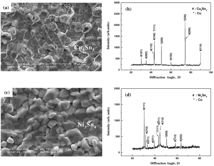
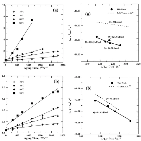
(3) Interfacial Reactions Between Sn–58 mass%Bi Eutectic Solder and (Cu, Electroless Ni–P/Cu) Substrate. 1823. rate was slower, Bi-containing layer was not observed. Figures 3(a) and (c) represent the top view of Cu6 Sn5 and Ni3 Sn4 intermetallic after the sample was aged for 70 days at 100◦ C, followed by solder etched away. The Cu6 Sn5 and Ni3 Sn4 intermetallic surface shown in Figs. 3(a) and (c) were then used to obtain the X-ray diffraction pattern of Cu6 Sn5 and Ni3 Sn4 intermetallic as shown in Figs. 3(b) and (d), respectively. On the Cu substrate, the hexagonal-shape intermetallic can be seen in Fig. 3(a). In contrast, the polygonalshape intermetallics are formed on the electroless Ni–P/Cu substrate as shown in Fig. 3(c). The thickness of the reaction layer in the diffusion couples can generally be expressed by the simple parabolic equation W = kt n. Fig. 2 SEM micrographs of the interface between (a) Sn–58Bi solder and Cu substrate, (b) Sn–58Bi solder and electroless Ni–P/Cu substrate aged at 120◦ C for 50 days.. hibited cracking within the intermetallic compound layer. The cracking occurred at the boundary between the region of the intermetallic compound with the Bi containing Cu6 Sn5 layer (Cu6 (Sn, Bi)5 ) and Cu6 Sn5 layer. According to the Sn–Bi binary phase diagram,14) the solubility of Bi in the Sn-phase increase rapidly from negligible at room temperature to about 9 at%Bi at 120◦ C. The Cu6 (Sn, Bi)5 intermetallic compound layer in this work contained a Bi content of 1–6 at% by EDX analysis. The source of the Bi containing layers is Bi rejected from the Sn-rich solder phase as it participated in the formation of the intermetallic layer. Therefore, in addition of the Bi atoms to the Cu–Sn intermetallic, the interface between Cu6 Sn5 and the Bi containing Cu6 Sn5 phase may be disrupt the local atomic arrangement, weaken the interfacial bonding, and then cause interfacial embrittlement. This trend would suggest that Bi-containing layer (Cu6 (Sn, Bi)5 ) decreased the ductility of the intermetallic compound. Similar result was also reported by Liu and Shang.15) The solid-state reaction between Cu and Sn–58Bi solder had been studied by Vianco et al.11) from 55–120◦ C for up to 400 days. They reported that the Cu6 Sn5 and Cu–Sn–Bi intermetallic compound formed as a result of the reactions, and found that the formation of the double-layers (Cu6 Sn5 /Cu– Sn–Bi) was due to the faster growth rate of Cu6 Sn5 intermetallic. This is due to the fact that the Bi atoms rejected from Sn-rich phase have no time to diffuse away from the interface so that a Cu–Sn–Bi compound formed. Also, this result was consistent with the result of Vianco et al.11) However, in Sn– 58Bi/electroless Ni–P/Cu system, since the Ni3 Sn4 growth. (1). where W is the thickness of the intermetallic layer; k, the growth rate constant; n, the time exponent; and t, the reaction time. Figure 4 shows the thickness of the intermetallic compound layer as a function of the square root of time for various aging temperatures. These intermetallic thicknesses were measured at every interval of time. The intermetallic compound layer thickness increased linearly with the square root of aging time and the growth was faster for higher aging temperatures. This is in agreement with previous works.12, 16–18) If the growth process were controlled by diffusion mechanism, the increase of the intermetallic compound layer after aging should follow the square root time law, W = kt 0.5 . It is empirically found that n takes the value of 0.5 when the reaction is mainly controlled by diffusion mechanism.19) Vianco11) and Chen12) studied the growth kinetics of the Cu6 Sn5 and Ni3 Sn4 intermetallic compound in Sn–58Bi solder and reported that the growth of these intermetallic compounds followed diffusion controlled kinetics. As shown in Fig. 4, the results are in good agreement with the diffusion controlled growth kinetics reported by previous workers.12, 16–18) The layer growth of the Ni3 Sn4 intermetallic is much slower than that of the Cu6 Sn5 intermetallic. The growth of Ni3 Sn4 intermetallic was very slow, with the layer thickness reaching only 1.82 µm after 60 days of aging at 120◦ C. This implies Ni–P deposits will be a very good diffusion barrier for the Sn–58Bi solder. The growth rate constant was calculated from a linear regression analysis of W versus t 0.5 , where the slope = k. Table 1 lists the growth rate constants calculated for the Cu6 Sn5 and Ni3 Sn4 intermetallic at different aging temperatures, respectively. Most of the linear correlation coefficient values (R 2 ) for these plots were greater than 0.96 except the low temperature (70◦ C). This good linear correlation suggests that the growth of the intermetallic compound layers is similar diffusion mechanism over the temperature range studied. The time exponent was evaluated using the equation representing the growth kinetics at each aging temperature as, Y = At n + B. (2). where Y is the layer thickness; t, reaction time; n, the time exponent; B, the layer thickness at t = 0; and A, the constant. This equation was converted into a logarithmic expression ln(Y − B) = n ln t + ln A. (3). The time exponent (n) was obtained from the slope of ln (Y −.
(4) 1824. J.-W. Yoon, C.-B. Lee and S.-B. Jung. Fig. 3. Top views and X-ray diffraction patterns of the intermetallic compound: (a), (b) Cu6 Sn5 and (c), (d) Ni3 Sn4 .. Table 1 Calculated the square of growth rate constants (k 2 ) and linear correlation coefficient (R 2 ). Solder/Substrate (Intermetallic). Temp. (◦ C). R2. k2 −19 (10 m2 /s). Sn–58Bi/Cu (Cu6 Sn5 ). 70 90 100 120. 0.85 0.97 0.98 0.96. 1.16 4.50 13.37 374.75. Sn–58Bi/ Electroless Ni–P/Cu (Ni3 Sn4 ). 70 90 100 120. 0.85 0.97 0.99 0.96. 0.14 0.75 1.91 4.99. B) versus ln t. Table 2 lists the time exponents determined by the linear regression analysis of each aging temperature using eq. (3). The diffusion processes appeared to be largely responsible for growth of the intermetallic compound layer, although the time exponents were not exactly 0.5. The following simple Arrhenius relationship was used to determine the activation energy for the layer growth of Cu6 Sn5 and Ni3 Sn4 intermetallic compound respectively; k 2 = k02 exp(−Q/RT ). (4). where k 2 is the square of growth rate constant; k02 , the frequency factor; Q, the activation energy; R, the gas constant; and T , the aging temperature. The activation energies were. Table 2 Time exponent (n) as a function of aging temperature. Solder/Substrate (Intermetallic). Temp. (◦ C). n. Sn–58Bi/Cu (Cu6 Sn5 ). 70 90 100 120. 0.68 0.47 0.49 0.66. Sn–58Bi/electroless Ni–P/Cu (Ni3 Sn4 ). 70 90 100 120. 0.48 0.44 0.54 0.33. calculated from the slope of the Arrhenius plot. Figure 5 shows the Arrhenius plots for the layer growth of the Cu6 Sn5 and Ni3 Sn4 intermetallic compound. The apparent activation energies for the layer growth of Cu6 Sn5 and Ni3 Sn4 intermetallic compound are 127.9 and 81.6 kJ/mol, respectively. The activation energies for the layer growth of Cu6 Sn5 and Ni3 Sn4 intermetallic compound reported by Vianco and Chen (which the author evaluated from Fig. 17 in Ref. 11) and Fig. 8 in Ref. 12), respectively) are also shown in Fig. 5. Table 3 lists the values of the activation energy (Q) obtained from the temperature dependence of k 2 , with the data from previous works. The Q-values for the growth of the Cu6 Sn5 and Ni3 Sn4 intermetallic found by Vianco et al.11) and Chen et al.12) were 55 ± 7 and 90 kJ/mol, respectively. The.
(5) Interfacial Reactions Between Sn–58 mass%Bi Eutectic Solder and (Cu, Electroless Ni–P/Cu) Substrate. 1825. Table 3 Activation energy for the growth of Cu6 Sn5 and Ni3 Sn4 intermetallic compound (IMC) together with values reported in previous works. Solder/Substrate Sn–58Bi/Cu. Sn–58Bi/Ni. Diffusion couple Prep. method. Temp. (◦ C)/Time (day). IMC Layer. Activation energy (Q, kJ/mol). Ref.. Spreading. 70–120◦ C/up to 60 days. Dipping. 55–120◦ C/up to 400 days. Cu6 Sn5. 127.9. This work. Cu6 Sn5. 55 ± 7. Spreading. 70–120◦ C/up. 11). to 60 days. Dipping. 85–120◦ C/up. Ni3 Sn4. 81.6. This work. to 150 days. Ni3 Sn4. 90. 12). Sn–3.5Ag/Cu. Practical solder joint. 70–170◦ C/up to 100 days. Total (Cu6 Sn5 + Cu3 Sn). 64.8. 20). Sn–3.5 Ag–0.75Cu/Cu. Practical solder joint. 70–170◦ C/up to 100 days. Total (Cu6 Sn5 + Cu3 Sn). 64.4. 20). Practical solder joint. 70–170◦ C/up. Total (Cu6 Sn5 + Cu3 Sn). 105.1. 21). Sn–37Pb/Cu. to 25 days. Fig. 4 Thickness of intermetallic compound layers with aging time: (a) Cu6 Sn5 and (b) Ni3 Sn4 .. Fig. 5 Arrhenius plot of the intermetallic compound layer growth: (a) Cu6 Sn5 and (b) Ni3 Sn4 ..
(6) 1826. J.-W. Yoon, C.-B. Lee and S.-B. Jung. diffusion couple of Vianco et al.11) and Chen et al.12) was prepared using hot dipping. Also, the diffusion couple of Chen et al.12) was assembled from Sn–58Bi solder and pure Ni. Thus, the discrepancy among the activation energies is due to the differences in the diffusion couples, aging conditions and analytical method used. In general the solder alloys with a high activation energy would be expected to grow slower at low temperatures and faster at high temperatures compared to those with a low activation energy. In this work, the activation energy of Cu6 Sn5 intermetallic due to the faster growth at high temperature exhibited higher than that of Ni3 Sn4 intermetallcs. As shown in Fig. 5(a), the lower temperature data (70, 90 and 100◦ C) exhibited an apparent activation energy of 84.2 kJ/mol and the higher temperature data (100 and 120◦ C) had a value of 203.8 kJ/mol. Combining the two data sets resulted in a value of 127.9 kJ/mol. The intermetallic layer data for the Sn–58Bi/Cu system suggest that two mechanisms were active over the temperature range of the analysis.10) The low activation energy (70–100◦ C) means that the rate controlling is the grain boundary diffusion. The initial condition for the growth model is the point where a continuous intermetallic layer is established. Nucleation and growth of individual grains occurs very rapidly. Once a continuous layer is established, additional growth requires diffusion of the reacting species (Sn and/or Cu) through the intermetallic layer. The grain structure of the intermetallic layer has a key influence on diffusion rate through the layer. In this study, also, the layers of Cu6 Sn5 and Ni3 Sn4 have a scalloped morphology. But the resulting activation energy of 127.9 kJ/mol is considered too high for Sn–58Bi/Cu system. Neglecting the 120◦ C data point would have an activation energy of 84.2 kJ/mol, which is a more reasonable number. Further work between 100◦ C and 120◦ C is required to fully clarify this point. 4. Conclusion The effect of isothermal aging (70, 90, 100 and 120◦ C) on the microstructure and intermetallic growth of Sn–58Bi solder/(Cu, electroless Ni–P/Cu) substrate were presented in this paper. The following conclusions were obtained: (1) The aged Sn–58Bi/Cu joint consists of the Cu substrate, the Cu6 Sn5 intermetallic, the Bi containing Cu6 Sn5 phase, the Bi-rich and Sn-rich phase. It found that the formation of the double-layer (Cu6 Sn5 /Bi containing Cu6 Sn5 ) was due to the faster growth of Cu6 Sn5 intermetallic. On the other hand, the Ni3 Sn4 intermetallic growth of Sn–58Bi/electroless Ni–P/Cu interface was slower, double-layer was not observed. (2) There was a linear relationship between the growth of the intermetallic layer thickness and the square root of the ag-. ing time. The good linear correlation of the results indicates that the formation of intermetallic compound layer is mainly controlled by diffusion mechanism. The growth rate of the Ni3 Sn4 intermetallic is much slower than that of the Cu6 Sn5 intermetallic. This implies Ni–P deposits will be a good diffusion barrier for the Sn–58Bi solder. (3) The apparent activation energies calculated for the growth of the Cu6 Sn5 and Ni3 Sn4 intermetallic are 127.9 and 81.6 kJ/mol, respectively. The activation energy of Cu6 Sn5 intermetallic due to the faster growth at high temperature exhibited higher than that of Ni3 Sn4 intermetallic. Acknowledgements This work was supported by grant No. (R01-2000-00227) from the Basic Research of the Korea Science & Engineering Foundation. REFERENCES 1) T. Takemoto, A. Matsunawa and M. Takahashi: J. Mater. Sci. 32 (1991) 4077–4084. 2) P. T. Vianco and F. J. Yost: Sandia Report, SAND 92-0211, Sandia Nat. Lab., April (1992) pp. 1–9. 3) C. B. Lee, S. B. Jung, Y. E. Shin and C. C. Shur: Mater. Trans. 42 (2001) 751–755. 4) J. Glazer: Int. Mater. Rev. 40 (1995) 65–93. 5) F. Hua, Z. Mei and J. Glager: Proc. of Electronics Components and Technology Conference, (1998) pp. 277–282. 6) C. H. Raeder, L. E. Felton, V. A. Tanzi and D. B. Knorr: JEM 23 (1994) 611–617. 7) Z. Mei and J. W. Morris, Jr.: JEM 21 (1992) 599–607. 8) W. J. Tomlinson and I. Collier: J. Mater. Sci. 22 (1987) 1835–1839. 9) L. E. Felton, C. H. Raeder and D. B. Knorr: JOM 45 (1993) 28–32. 10) P. T. Vianco, P. F. Hlava and A. C. Kilgo: JEM 23 (1994) 583–594. 11) P. T. Vianco, A. C. Kilgo and R. Grant: JEM 24 (1995) 1493–1505. 12) C. Chen, C. E. Ho, A. H. Lin, G. L. Luo and C. R. Kao: JEM 29 (2000) 1200–1206. 13) P. Shewmon: Diffusion in solids, 2nd Edn., (TMS, Pennsylvania, 1989) pp. 71–75. 14) T. B. Massalsk: Binary Alloy Phase Diagrams, Vol. 1, (ASM, Ohio, USA, 1986) pp. 794–796. 15) P. L. Liu and J. K. Shang: Scr. Mater. 44 (2001) 1019–1023. 16) R. F. Pinizzotto, E. G. Jacobs, J. A. Sees, L. A. Foster and C. Pouraghabagher: JEM 22 (1993) 355–359. 17) K. N. Tu and R. D. Thompson: Acta Metall., 30 (1982) 947–952. 18) P. J. Kay and C. A. Mackay: Trans. Inst. Metal Finishing 54 (1976) 68–74. 19) J. Burke: The Kinetics of phase transformations in metals, translated from English by K. Hirano and H. Hori (Kyoritsu, Tokyo, 1972) pp. 190. 20) C. B. Lee, S. J. Suh, Y. E. Shin, C. C. Shur and S. B. Jung: Proc. 8th Symposium on Microjoining and Assembly Technology in Electronics (mate, 2002) pp. 351–356. 21) Y. C. Chan, Alex C. K. So and J. K. L. Lai: Mater. Sci. Eng. B55 (1998) 5–13..
(7)
Figure
Related documents
The interfacial reaction between Sn–36Pb–2Ag (numbers are all in mass% unless specified otherwise) solder balls and Ni, Ag and Ni/Ag electroplated on a Cu substrate was investigated
