Quadrature Power Amplifier for
RF Applications
C.H. Li MSc. Thesis November 2009
Supervisors: prof. dr. ir. B. Nauta dr. ir. R.A.R. van der Zee dr. ing. E.A.M. Klumperink Report number: 067.3338 Chair of Integrated Circuit Design Faculty of Electrical Engineering, Mathematics & Computer Science University of Twente P. O. Box 217
Abstract
new power amplifier (PA) architecture is proposed as a more power efficient way to amplify modulated signals at radio-frequencies (RF) compared to conventional polar power amplifiers.
Polar PA’s, using the Envelope Elimination and Restoration (EER) linearizing technique for high efficiency switch mode amplifiers provide amplification for modulated signals at RF with high efficiency and linearity. However, such systems require high alignment between phase and amplitude signal paths and the bandwidth of the amplitude path needs to be three to four times the RF-bandwidth. The latter directly translates to high power consumption.
Instead of decomposing the quadrature signals to a phase and amplitude signal set, suggested is that the quadrature signals are to be directly amplified using a quadrature power amplifier. The lack of a separate phase and amplitude signal path avoids the linearity and bandwidth requirements, thus reducing power consumption. A possible quadrature PA architecture is presented. This architecture consists of two supply modulated switch mode amplifiers placed in a bridge and is capable of handling negative voltages, modulation and power combining at RF. Furthermore, a driver architecture is presented to properly drive the quadrature PA.
Simulations results of the quadrature PA using 90nm CMOS models show a functional quadrature PA model with a power added efficiency of 30% at 6.4dBm output power driven at 2.4GHz and a maximum input power at 10MHz and 25% at 5.1dBm output power at 50MHz.
Preface
f you just study long enough, eventually you don’t even know what a resistor is anymore”, said by Ir. M.G. “Rien” van Leeuwen during first year electronics course “EL-BAS”. Now, almost ten years ago and I found these words to be very true in the years to follow. Especially the last year, as I started working on my master assignment, till what is now this thesis, from time to time I “forgot what a resistor was”. And from there on in, the only way to avoid insanity is to go one or more steps back. In the end, I think this characterizes not only my master assignment, but my total study career at the University Twente; two steps forward and one step back.
Though slowly, but steady, always avoiding insanity, I could not have finished my master without the help of the people I met through the years. Especially this last year and I want to thank the people of floor 3, the ICD and SC people for their support, cheerful good mornings or colorful discussions about food, politics, music, motorcycles and sometimes electronics. I want to thank head of chair, Bram Nauta, especially for giving me the opportunity to go to Japan for my internship and my direct supervisor Ronan van der Zee for his seemingly endless patience. And last, but not least, I want to thank my fellow master students Pieter Koster and Mark Ruiter: take care of my plant, will you ?
Chen-Hai Li “foxhole 3120” 18 November 2009
“The more I learn, the more I realize I don’t know”
Contents
1. Introduction 9
2. Power amplifiers 11
2.1. Introduction 11
2.2. Efficiency 11
2.3. Linear mode amplifiers 12
2.3.1 Class A 13
2.3.2 Class B 13
2.3.3 Class AB 14
2.3.4 Class C 14
2.4. Switch-mode power amplifiers 15
2.4.1 Class-D 15
2.4.2 Class E 16
2.5. Linearization techniques for power amplifiers 19
2.5.1 Envelope Elimination and Restoration 19
2.5.2 Linear Amplification with Non linear components (LINC) 21
3. Quadrature Power Amplifier 23
3.1. Introduction 23
3.2. Quadrature signals and quadrature PA concept 23
3.3. Choice of PA configuration in quadrature PA system 27
3.4. Quadrature PA model with switches 31
3.5. Quadrature PA model with transistors for positive or negative supply 37 3.6. Quadrature PA model for both positive and negative supply 42 3.7. Quadrature PA model with transistors for positive and negative
supply voltages and bulk switches 46
3.8. Losses and sizing 53
3.8.1 Conduction losses 54
3.8.2 Switching losses 55
3.8.3 Direct path current losses 55
3.8.4 Sizing 56
3.9. AM-PM Distortion 59
3.10. Driver 61
3.10.1 Design issues of a quadrature PA driver 61
4. Simulations 69
4.1. Introduction 69
4.2. Technology and models 69
4.2.1 Signal set 70
4.3. Device and component dimensions 72
4.3.1 Introduction 72
4.3.2 Quadrature PA without bulkswitches 72
4.3.3 Quadrature PA with bulkswitches 73
4.3.4 Driver 74
4.4. Testbench 75
4.4.1 Introduction 75
4.4.2 Transient 75
4.4.3 Quasi-periodic steady state analysis 75
4.4.4 16-QAM analysis 76
4.4.5 Output bandwidth 76
4.4.6 Power added efficiency 77
4.5. Simulation Results 78
4.5.1 Transient simulation results 78
4.5.2 Quasi-periodic steady state simulation results 81
4.5.3 16-QAM simulation results 83
4.5.4 Quasi-periodic AC simulation results 89
4.5.5 Power added efficiency performance 90
5. Conclusions 91
6. Recommendations 93
1.
Introduction
or mobile communication systems the transceiver is the key block, for a transceiver, made up from the words transmitter and receiver, sends and receives signals to and from the antenna, making wireless communication possible. Early radio transceivers date from the 1900’s, such as Hughes’ Morse induction machine and Edison’s broadcast over the Lehigh Valley Railroad. The following years, other researches including people like Hertz, Faraday, Maxwell and Tesla contributed to the theory of electromagnetism and wave-theory, making it possible for people like Armstrong, to construct transceivers concepts which are still used today.
Figure 1 typical RF transmitter with direct conversion architecture
Pushed by the technological revolution of the past decades these wireless systems have evolved from simple Morse code transceivers to complex systems. With the help of digital computing on chip, complex (de-)modulation is possible, leading to quadrature up- and down-conversion architectures. A commonly used architecture is the direct conversion architecture as shown in Figure 1 [19][20].
Still, a power amplifier (PA) remains a power hungry block. In a time where smart usage of energy resources is not only cost wise, but also environmentally wise, the need for architectures with a less power consuming power amplifier is desired. This thesis presents a new concept and model for a possible more power efficient power amplifier architecture. In the following chapter power amplifiers in general and linearization techniques are discussed. A step for step design that leads to a model for the quadrature power amplifier is given in chapter 3. Chapter 4 deals with specifications, simulations and results. Lastly, conclusions and recommendations are found in chapters, 5 and 6.
2.
Power amplifiers
2.1.
Introduction
n a RF transmitter, the message signal undergoes several steps such as digital signal processing, digital to analog conversion and filtering. The last step between up conversion of the baseband signal to RF frequencies and the antenna is the amplification of the signal. Specified for different communication standards, the signal has to be amplified to a certain power level so that it can be transmitted, received and decoded within a fixed geographical region. In contrast to small signal amplifiers, these amplifiers have to deliver serious amount of power, hence the commonly used term power amplifier (PA).
Traditionally power amplifiers (PA’s) have been categorized in classes; A, B, C, D, E, etc. A second distinction can be made on the operating character of the active device: acting as a current source or as a switch. The “classic” classes A, B, A/B and C belongs to the first group. Classes D and E belong to the latter.
First the power efficiency of power amplifiers is discussed (§2.2). Following is an overview of the different classes and modes (§2.3 and §2.4). The discussion of the Envelope Elimination and Restoration (§2.5.1) and the Linear Amplification with Non-Linear Components (§2.5.2) linearization techniques concludes this chapter.
2.2.
Efficiency
The conventional way of designing PA’s is not to achieve maximum power transfer, but aiming for high efficiency. One might say that maximum power transfer makes logic sense, figuring the large amount of power needed to drive the antenna, but a PA with a conjugate match, the efficiency would be 50% maximum. Not only is this value unacceptable low, but also offers practical problems. An efficiency of 50% means that the same power dissipated in the load, will also be dissipated in the circuit. Considering the relatively large amounts of power needed to drive the antenna, this would give rise to thermal problems of the circuit itself. For nowadays applications such as cellphones and other portable communication devices this would be quite troublesome. [1][3]
Instead of aiming for maximum power transfer, PA’s are designed for the highest possible efficiency while maintaining an acceptable gain and linearity. The
efficiency is therefore the performance parameters mostly used for power amplifiers. Two metrics for efficiency are used: drain efficiency, which is defined as the ratio between the power delivered to the load and the power delivered by the supply:
out
dc P
P
η= (1)
Drain efficiency can give high efficiency for PA’s that have no power gain. To overcome this, a second metric was introduced: power added efficiency (PAE). The power added efficiency is defined as the ratio between the difference of the RF output and input power and the power delivered by the supply.
out in
dc
P P
PAE
P
−
= (2)
It can be seen that the PAE is lower than the drain efficiency. For PA’s with relatively high power gains the PAE becomes equal to the drain efficiency.
2.3.
Linear mode amplifiers
[image:14.612.223.418.468.614.2]When the device acts as a current source, the transistor is biased in such a way that it drives in saturation. Sometimes called linear mode amplifier, however the input output relation can have a very non linear characteristic.
Figure 2 typical RF power amplifier configuration
Power amplifiers for RF with the transistor acting as a current source all have the same basic circuit. In this general model, shown in Figure 2, the output power is delivered to the load, modeled by resistor RL. A “big” inductor or radio-frequency
and application a load network is used e.g. to shape signals or use impedance transformations to maximize power efficiency. Historically, power amplifiers are primarily distinguished in terms of which part of the RF input cycle the transistor conducts. This conduction angle classifies linear mode amplifiers in classes A, B, AB and C.
2.3.1 Class A
A class-A power amplifier can be regarded best as a textbook small signal amplifier suited for large signals. As shown in Figure 3, the transistor is biased in such a way that it is active for the total RF cycle: the conduction angle for a class-A PA is 360°.
Figure 3 typical class-A power amplifier configuration
The transistor is biased depending on its input as the bias voltage is set so that the corresponding output will never turn the transistor off. The output swing is therefore maximized while providing high linearity and high gain.
However the class-A PA has a constant quiescent current even when there is no signal. Also, to reduce distortion large currents and high voltages are needed. This results in high power consumption. The power efficiency of a class-A PA is therefore quite low. The theoretical maximum efficiency is 50%, in practice 35% and when really high linearity is needed, the efficiency is lower than 25% [1].
2.3.2 Class B
Figure 4 typical class-B power amplifier in push-pull configuration
Having simultaneously a drain current and voltage of zero for a fraction of the RF cycle, thus reducing transistor dissipation, increases the efficiency. For a class-B, the theoretical efficiency is 78.5% [1][3]. However, such high efficiency is only at maximum output power. Overall efficiency will be lower for transmitting at less than maximum power. Though a class-B amplifier has improved power efficiency regarding to class-A amplifiers, the costs is less linearity [4].
2.3.3 Class AB
A class AB is the best of both worlds. Its configuration is a class-B PA, but instead of biasing the transistor at cut-off, a small fraction of bias currents is allowed. Thus while maintaining efficiency approximating class-B, a linearity approximating class-A is achieved. Depending on the linearity and efficiency requirements the bias level of the class-AB PA is determined.
Theoretically the efficiency and linearity performance depending on bias level, can be anything in between full class-A or full class-B.
2.3.4 Class C
2.4.
Switch-mode power amplifiers
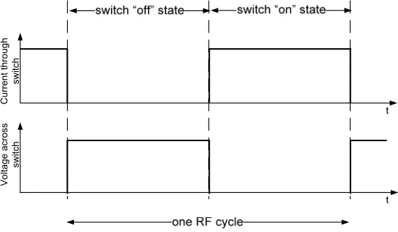
[image:17.612.151.436.188.354.2]In switch-mode amplifiers the active device acts as a switch. The idea behind using switches is that an ideal switch doesn’t dissipate power, for there is either zero voltage across or zero current through the switch. Thus the voltage-current product is zero, the transistor dissipates no power and efficiency is 100%. This is shown in Figure 5.
Vo
ltage acr
oss
swi
tc
h
Current through
sw
itc
h
Figure 5 voltage and current relation of an ideal switch-mode transistor
Unlike linear-mode power amplifiers the output signal is not intended to be a replica of the input. Thus not the conduction angle, but the way the voltage and current waveforms are shaped is the primary distinction between the switch-mode power amplifiers classes. Of the three conventional switch-mode PA classes; class D, E and F only the first two are discussed.
2.4.1 Class-D
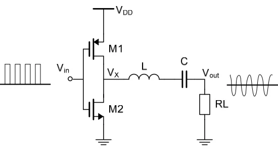
Figure 6 typical class-D power amplifier configuration
Figure 6 shows a basic class-D circuit, NMOST and PMOST transistors act as a switch like an inverter output stage, switching between the supply and ground, generating a rectangular voltage waveform. An LCR network acts as the tuned output filter. A properly tuned load network will have a low reactance to the fundamental and high impedance for the harmonics, resulting in a sinusoidal output across the load. This load, i.e. the antenna is modeled by resistance RL.
The transistors operate in a push pull configuration, similar to class-B, but are driven so hard that they operate as switches. A gate bias is not needed, but the input signal must be sufficient to drive the transistors in triode and cut-off at the right time of the RF-cycle.
Ideal switches dissipate no power due to infinite switching time. A tuned LC network doesn’t dissipate power as well. Thus, theoretical the efficiency of an idealized class-D PA is 100%. However ideal switches do not exist. Real switches exhibit finite switching time. Such real life devices will exhibit time overlap between voltages across and current through the switches, dissipating power, reducing efficiency. Furthermore, conduction losses in transistor on-resistance and component resistance as well as capacitive switching losses due to drain capacitances will reduce the efficiency even more.
2.4.2 Class E
Figure 7 typical class-E power amplifier configuration
Figure 8 typical voltage and current waveforms for a class-E PA
Figure 7 and Figure 8 show the classic class E circuit and its typical waveforms. The amplifier consists of a switched operated transistor that is “on”, with no voltage across it, or is “off”, with no current through it. The radio frequency choke (RFC) is assumed large enough so that the current IL flowing through is constant. The quality
that the voltages across and currents trough the active device satisfy a set of conditions; 1) At the turn off state, VX is delayed until the current drops to zero, 2)
At the turn on stage, VX returns to zero, before the current increases and 3) the slope
of VX is near zero at the turn on stage of the switch. The result is that the
waveforms never have simultaneously high voltage and high currents. This yields in lower power dissipation, thus a higher efficiency.
The derivation of the design equations can be found in [6] and a more elaborate discussion and more specific approximation in [5]. The basic forms are as follows:
2 2 2 2 0.577 1 4 DD DD V V R
P π P
⎛ ⎞ ⎜ ⎟ = ⎜ ⎟= ⎜ + ⎟ ⎜ ⎟ ⎝ ⎠
2 / 2
L =QR π f
2
1
1 5.447
1
2 4 2 2
C = πfR⎛⎜π + ⎞⎛ ⎞⎟⎜ ⎟π = π fR
⎝ ⎠ ⎝ ⎠ 2 2 2 1 1.42 1
(2 ) 2.08
C
f L Q
π
⎛ ⎞⎛ ⎞
≈⎜ ⎟⎜ + ⎟
−
⎝ ⎠
⎝ ⎠ (3)
The R denotes not only the load resistance, but the total resistance in the system, P the wanted output power and Q denotes the quality factor of the load network. Though the voltage has zero slope at turn off, the current is almost maximum. It is shown that the peak drain current is roughly 1.7VDD/R. [3][4]. This means that if
the switch is not fast enough, there is still high switch dissipation. Also, a real switch exhibits an on-resistance. In practice this means that a switch has a nonzero “on” voltage.
Another property of the class-E PA is that it exhibits a large peak voltage in the off state approximately 3.56VDD-2.56Vmin, with Vmin the minimal voltage across the
transistor. This demands the usage of devices with a higher breakdown voltage than the voltage given for used technology. Because of afore mentioned reason, a class-E is quite demanding of its switch specifications.
2.5.
Linearization techniques for power amplifiers
As the most efficient power amplifiers are normally nonlinear, the needs for linearizing techniques arise in many RF applications to restore linearity. Two linearization techniques will be shown in the following paragraphs: envelope elimination and restoration (EER) and linear amplification using non-linear components (LINC). The first will be the direct motivation for the quadrature power amplifier architecture to be presented in chapter 3. The latter shows several concepts which show similarities with the presented power amplifier and is therefore mentioned.
2.5.1 Envelope Elimination and Restoration
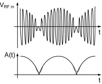
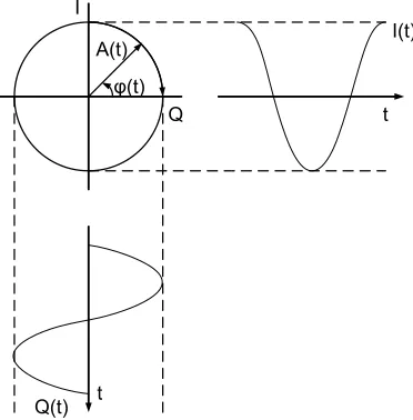
Envelope Elimination and Restoration (EER) was first proposed by Kahn in 1952 and is also called polar modulation. The basic principal is that bandpass signals can be regarded as a result of amplitude modulation and phase modulation. This can be seen by describing a modulated RF signal in terms of quadrature signals:
( ) ( )sin( ) ( ) cos( )
Vrf t =I t ωt +Q t ωt (4)
Defining the quadrature components I(t) and Q(t) as: I(t)=A(t)sin( (t)) Q(t)=A(t)cos( (t))
φ φ
and
2 2
( ) ( ) ( )
( ) ( ) arctan
( )
A t I t Q t
Q t t
I t
φ
= +
=
This leads to:
( )[sin( ( ))sin( ) cos( ( )) cos( )]
Vrf = A t φ t ωt + φ t ωt (5)
From this follows the general form of a modulated signal:
( ) ( )sin( ( ))
Vrf t =A t ω φt+ t (6)
In this form A(t) is the amplitude modulation and φ(t) the phase modulation of the signal.
Figure 9 envelope elimination and restoration
Figure 9 illustrates this concept. An RF bandpass signal drives an envelop detector and a limiter, such that the amplitude and phase signals are separated. Each signal is amplified and combined in the PA, hence the name envelope elimination and restoration. If a switch mode PA, i.e. class-D or class-E is used, the output current flowing through drain is a direct function of the envelope, thus the supply of the PA is modulated with the amplitude. Because of the constant amplitude of the phase signal φ(t), the phase information will hardly be distorted by the non-linear amplifier. A transistor operating as a current source transistor is not suitable for amplitude modulation using voltage supply modulation, because the current is not a direct function of the voltage supply. [1][3].
The advantage is that a polar modulator requires less linearity at the PA level, since the linearity requirements are shifted to the amplitude path and the phase path. However, several other requirements are needed to prevent linearity degradation. The first is the need for a low differential delay between the amplitude and phase signal path. The envelope and phase signal have each their own path, operating at their own frequencies. A mis-timing of both signal paths in the PA modulator gives rise to distortion [10][11].
Figure 10 input and envelope signal in an EER system. The straight line corresponds with ideal behavior, the dotted line with finite envelope modulator bandwidth
Though EER loosens the linearity requirements of the PA, the PA still deals with issues such as AM-PM conversion due to drain capacitances and the modulating drain voltage of the transistor, as well as AM-AM conversion due to on-resistance of transistors. A short overview of several polar PA’s found in literature are shown in Table 1.
ref-erence
year technology application PAE peak
output power
[8] 1998 0.8mm CMOS 800-900 MHz 49% 29.5 dBm
[9] 2005 GaAs HFET 2.4 GHz 28% 19 dBm
[15] 2005 0.18μm CMOS 1.75 GHz GSM-EDGE 34% 27 dBm
[7] 2008 5W LDMOSFET 1 GHz 39.5% 31.7 dBm
[16] 2008 GaAs MESFET 1 GHz 68% 27 dBm
Table 1 overview of polar designs in literature
2.5.2 Linear Amplification with Non linear components (LINC)
Figure 11 linear amplification using non-linear components
Figure 11 shows a block diagram of a possible LINC implementation. First the RF signal decomposed in two vector signals. Figure 12 shows the signal constellation for this situation. The two vectors signals S1 and S2, are constant amplitude, phase
modulated. Each signal is amplified with two identical amplifiers. After recombining, the result is the sum of the two vectors, producing an amplified output signal.
φ1
φ2
S
1S
2V
outFigure 12 typical signal composition for LINC PA
Though LINC avoids the amplitude variation problem in a PA, it has a few drawbacks. First is the generation of the two vector signals S1 and S2. These are
3.
Quadrature Power Amplifier
3.1.
Introduction
nvelope elimination and recombination offers a linearization technique to optimize power amplifiers in for example a direct conversion PA system to handle amplitude modulated signals with higher power efficiency. However, drawbacks such as differential delay in the signal paths and the bandwidth requirements for the envelope, as well as linear requirements for the switch-mode amplifier can degrade performance. Also, the design is not so straightforward since it needs several operating blocks such as an envelope detector, envelope modulator and a limiter.
A possible way to overcome these problems is to operate the PA in a quadrature configuration. Instead of decomposing the quadrature signals to a phase and amplitude signal set, the quadrature signals are to be directly amplified and modulated using a quadrature power amplifier. The lack of a separate phase and amplitude signal path avoids the linearity and bandwidth requirements
In the following paragraphs this concept is explored, discussing the basic idea and choice of PA class to start with (§3.2 & §3.3). Following is a detailed discussion about modeling and designing the quadrature power amplifier architecture (§3.4, §3.5, §3.6 and §3.7). About losses and sizing of the final architecture can be found in §3.8 and a short word on AM-PM distortion can be found in §3.9. The final paragraph deals with the driver architecture to proper drive the quadrature PA (§3.10).
3.2.
Quadrature signals and quadrature PA concept
As shown in §2.5.1, the general form of a modulated signal is described as:
( ) ( )sin( ( ))
Vrf t = A t ω φt+ t (7)
But written as:
( ) ( ) cos( ( ))
Vrf t = A t ω φt+ t (8)
the modulated RF signal can be written as:
( )[cos( ( )) cos( ) sin( ( ))sin( )]
Vrf = A t φ t ωt − φ t ωt (9)
using
I(t)=A(t)cos( (t)) Q(t)=A(t)sin( (t))
φ φ
resulting in:
( ) ( ) cos( ) ( )sin( )
Vrf t =I t ωt −Q t ωt (10)
[image:26.612.241.394.328.437.2]This result shows that a modulated RF signal can also be expressed as a subtraction of two modulated quadrature signals I(t) and Q(t). This is valid as since both (7) and (8) can be used to describe modulated signals.
Figure 9 shows a possible block diagram of such quadrature modulator scheme. Two message signals, I(t) and Q(t) are mixed with a local oscillator with a 90° phase shift with respect to each other. A subtraction is used to obtain the signal as according to (10).
Figure 13 quadrature modulator
Though more common as addition as in (4), this concept of quadrature modulation
can be found in widely used systems as digital modulation schemes and correlation receivers and can be extended to power amplifiers.
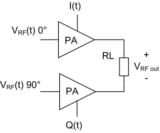
RL
Q(t) PA
PA
VRF(t) 0°
VRF(t) 90°
I(t)
+ VRF out
[image:26.612.238.396.547.678.2]
Figure 14 shows this concept for a power amplifier system. The most basic form consists of two quadrature modulated PA’s, 90° phase difference in bridge mode. Unlike traditional EER, each PA amplifier is driven by constant amplitude, constant phase, carrier signal and the voltage supply is modulated with either I(t) or Q(t) signal. The load in the bridge, e.g. an antenna senses the difference between the modulated outputs of each PA, thus a subtraction is realized.
Since each PA is driven by a constant amplitude and constant phase RF carrier signal, only the quadrature signals I(t) and Q(t) contains information. This eliminates the need for matching between an envelope and a phase paths as is the case for conventional EER.
Secondly, since there is no envelope path that has to match with a much higher bandwidth phase path, the need for a wideband envelope path is redundant. This implies, that the bandwidth of the signal in a quadrature PA system, determined by the quadrature signal I(t) and Q(t), is much lower than the limited bandwidth of the envelope modulator as with an EER system.
The output voltage as seen at the load terminals can easily be predicted using an I-Q constellation diagram. Shown in Figure 15, mapping the I(t) waveform on the y-axis and the Q(t) waveform on the x-y-axis, the resulting envelope output amplitude and phase of the RF carrier signal can be reconstructed. Suppose I(t) and Q(t) are sinusoid with 90° phase difference, the resulting output will be an RF carrier signal with a constant amplitude.
I(t)
Q(t)
t
t I
Q A(t)
[image:27.612.198.384.415.604.2]φ(t)
Figure 15 quadrature signal constellation
the RF frequency. As the quadrature signals differ 90° in phase, the negative frequency component is cancelled out. This results in a single sideband carrier suppressed (SSSR) modulation, which in this case as mentioned, is a single frequency shifted up with the quadrature bandwidth.
Figure 16 spectrum of the RF signal (HRF), sinusoidal quadrature signals (HI and HQ) and the
resulting output (Houtput)
The downside of using a quadrature configuration is the mismatch between the I- and Q side in amplitude or phase. The result is a corrupted reconstruction of the RF message signal, downgrading overall performance. This mismatch can happen at several stages in the transmitter. At the power amplifier stage mismatch could occur for example when the RF input is multiplied with the quadrature signals resulting in amplitude mismatch or difference in path lengths resulting in phase mismatch. On the subject of quadrature mismatch much is written and numerous techniques can be found in literature which have reasonable results [21][22][23].
Quadrature mismatch is thus a quite common problem, but just as all mismatch related problems, doesn’t need to be a limiting factor to forsake the use of quadrature architectures.
Just as in Linear Amplification Using Non Linear Components (LINC), such a power combiner is a critical stage in the design, since a quadrature PA will also be sensitive to mismatch between the two signal paths.
Regarding power combiners, a limited number of articles can be found in literature. Most of the mentioned techniques use either quarter wave length transmission lines or transformers. The use of the former changes the voltage character of a system output to a current character. The result is that output of the different stages can be connected if it were current sources. The downside is that a quarter wavelength is impossible to implement on-chip. The use of transformers has a more widespread use operating at the gigahertz region. However to keep losses at a minimum, a high quality factor of the transformer is needed. This will mean that the components are relatively big, consuming major chip area or give rise to the need for using off-chip components.
Additionally, besides power combining, a transformer can also operate as impedance transformation. This will make the use for lumped LC impedance transformation network superfluous [24][25][26][27].
3.3.
Choice of PA configuration in quadrature PA system
In a quadrature PA system as described in the previous paragraph, the PA modulates an RF carrier signal with the quadrature signals I(t) and Q(t). The simplest way to achieve this is to use a switch mode amplifier such as class-D or class-E. These configurations are easily suitable for supply voltage modulation. Driving the amplifier with a hard switching RF signal and using the quadrature signal as supply voltage should generate the wanted modulated RF signal.
Supply modulation using a linear mode amplifier such as class-A or class AB, would be impossible since the output current is not a direct and linear function of the voltage supply. Modulating and driving such PA configuration would involve a more complicated configuration.
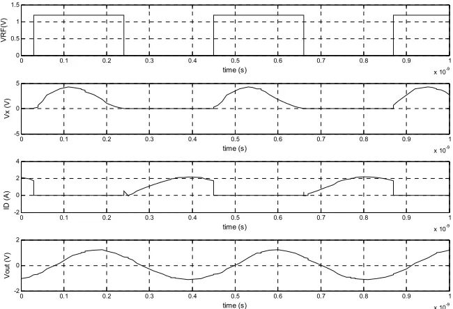
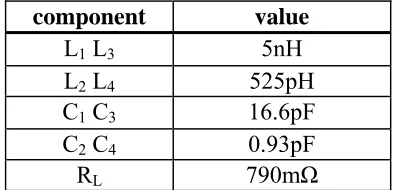
Of the two switch mode power amplifiers, the class-E favors because of its higher efficiency. However, it is unusable in a quadrature bridge configuration. Suppose the single end class-E power amplifier model using ideal switches with infinite high open resistance, neglectable low closed resistance of 1mΩ, no parasitic switch capacitances and infinitely small switching times. The switch is driven with a hard switching, 2.4Ghz, 50% duty cycle, RF pulse signal and the supply is connected to VDD=1.2V. The output should thus be a sinusoid with amplitude VoutI=1.2V. The
RF-choke inductor L1 is assumed to be large enough, the wanted output power is
Pout=1W and the quality factor of the tank is Q=10. The component values are
found using the Sokal formulas of (3) as given in §2.4.2 and are listed in Table 2.
The characteristics waveforms are shown in Figure 18 and correspond to the
Figure 17 single end class-E PA
component value
L1 5nH
L2 525pH
C1 16.6pF
C2 0.93pF
RL 790mΩ
Table 2 component values of a single end class-E PA.
0 0.1 0.2 0.3 0.4 0.5 0.6 0.7 0.8 0.9 1 x 10⁻⁹
0 0.5 1 1.5
time (s)
VRF
(V
)
0 0.1 0.2 0.3 0.4 0.5 0.6 0.7 0.8 0.9 1 x 10⁻⁹
-5 0 5
time (s)
Vx
(V
)
0 0.1 0.2 0.3 0.4 0.5 0.6 0.7 0.8 0.9 1 x 10⁻⁹ -2
0 2 4
time (s)
ID
(A
)
0 0.1 0.2 0.3 0.4 0.5 0.6 0.7 0.8 0.9 1 x 10⁻⁹
-2 0 2
time (s)
V
out
(
V
)
Now, suppose the configuration of Figure 19. Using two identical class-E amplifiers of Figure 17 and placed in a bridge. Again, each side is driven with a hard switching, 2.4Ghz, 50% duty cycle, RF pulse signal but the right, Q(t)-side of the bridge lags 90° in phase in respect with the left, I(t)-side. The supply is modulated with a constant supply voltage at VDD=1.2V. The output across the load RL, between
the nodes VoutI and VoutQ should be a sinusoid with constant amplitude of
√(VDD2+VDD2).
The RF-choke inductors L1 and L3 are assumed to be large enough, the wanted
output power is Pout=1W and the quality factor of the tank is Q=10. The
components value are found using the Sokal formulas of (3) as given in §2.4.2 and
are listed in Table 3.
[image:31.612.197.395.447.542.2]
Figure 19 ideal operation of a class-E power amplifier using ideal switches in bridge mode
component value
L1 L3 5nH
L2 L4 525pH
C1 C3 16.6pF
C2 C4 0.93pF
RL 790mΩ
Table 3 component values of Class-E PA in bridge mode
Compared to the waveforms of a single end class-E power amplifier, the waveforms of the bridged class-E power amplifier show differences, while they should be the same. Both the left as the right side show not the correct voltage and current waveform characteristics as in Figure 18. Furthermore, both sides don’t show equal waveforms. The result is not the expected voltage waveform across the load.
ground. This would be no problem if the class-E amplifiers would have a voltage source characteristic, but they tend to have a more current source characteristic due to the RF-choke.
This is made evident as the current through switch S2 is negative, indicating that the current is flowing in opposite direction. This results from the aforementioned nett current forced to either side in the bridge In this case to the right side, since the I(t)-side leads and Q(t)-I(t)-side lags. Reversing the phase difference, results in that the nett current will flow to the left or I(t)-side.
0 0.1 0.2 0.3 0.4 0.5 0.6 0.7 0.8 0.9 1
x 10-9
0 0.5 1 1.5 time (s) VRF (V )
0 0.1 0.2 0.3 0.4 0.5 0.6 0.7 0.8 0.9 1
x 10-9
-2 0 2 4 time (s) VX I (V )
0 0.1 0.2 0.3 0.4 0.5 0.6 0.7 0.8 0.9 1
x 10-9
-5 0 5 time (s) ID I ( A )
0 0.1 0.2 0.3 0.4 0.5 0.6 0.7 0.8 0.9 1
x 10-9
-2 0 2 4 time (s) VXQ ( V)
0 0.1 0.2 0.3 0.4 0.5 0.6 0.7 0.8 0.9 1
x 10-9
-5 0 5 time (s) ID Q ( A )
0 0.1 0.2 0.3 0.4 0.5 0.6 0.7 0.8 0.9 1
x 10-9
[image:32.612.149.474.205.539.2]-4 -2 0 2 4 time (s) VR L ( V)
Figure 20 waveforms for two class-E PA in bridge mode
Also, as shown in [5] the voltage at VXI indicates at a too low value for C1 and C2,
while the voltage at VXQ indicates a too high value for C3 and C4.
A nett-current in bridged class-E PA leads thus to unexpected voltage-current relation with non-tuned components. This results in the output voltage across the load, VRL as shown in Figure 20. It shows a waveform that not even resembles a
sinusoid.
words, a class-D will be suitable to operate in bridge mode for a quadrature PA system.
3.4.
Quadrature PA model with switches
As shown, a quadrature power amplifier is configured as two voltage supply modulated switch-mode power amplifiers placed in a bridge, operating at 90° phase difference. A class-E is unsuitable, but a class-D is, because its voltage characteristic enables any nett current caused by the 90° phase difference to flow back in the supply. Therefore, the class-D architecture will be the basic form of the quadrature power amplifier model.
In a class-D PA the transistors operate in switch-mode. The PA can therefore easily be modeled with switches. Using ideal switches with infinite high open resistance, neglectable low closed resistance, no parasitic switch capacitances and infinite switching times, a first order model can be realized omitting all high order effects. This is done to gain a principle insight of the operation of the quadrature PA.
Figure 21 single end quadrature power amplifier using ideal switches
Using ideal switches, the modulating switching PA can be modeled as Figure 21. As a quadrature PA needs two amplifiers in bridge mode, a single amplifier will be denoted as a single end quadrature PA. Operating as a class-D, the PA is driven with a hard switching RF signal, between zero and VDD=1.2V, with a duty cycle of
50% in such a way that either one switch is open and the other closed or vice versa, but never open or closed simultaneously. If the RF signal is zero the output is connected to the supply rail and if VDD, the output is connected to ground. The
supply is modulated with a baseband quadrature signal I(t), which in this case is sinusoid with from VDD=1.2V to VSS=-1.2V. The result at node VX is an RF pulse
Just as for a conventional class-D PA, a tuned network is used to produce a harmonic waveform across the load, modeled by resistor RL. For this network,
again just as in a conventional class-D PA a first order LC network can be used, as shown in Figure 21.
The filter is tuned to the RF frequency according to:
1
LC
ω = (11)
The quality factor of a series LCR network is defined as the ratio of energy stored to the energy lost per unit time and can be expressed as:
L Q
R
ω
= (12)
[image:34.612.224.404.395.515.2]Another definition of the quality factor is the steepness of the frequency response of the filter. An LCR filter thus resonates at the tuned frequency and usually exhibits a bandpass transfer function. The quality factor is the ratio between the tuned frequency and the -3dB bandwidth.
Figure 22 frequency response of LCR network
A too low Q can result in a low suppression of the higher harmonics, a too high a Q can result in large inductorvalues. A large inductor is not only difficult to make on-chip, but will also mean higher component resistance resulting in lower power efficiency. Furthermore, for a series LCR network at resonance, the voltage across the inductor or capacitor is Q times as great as that of the resistor. To limit these high voltages in the system it is preferable to keep the Q at minimum [3].
Using (11) and (12), the filter can be dimensioned. The only free parameter to
choose is the quality factor Q, L and C, since the resistor RL models the 50Ω
For simulation purposes a quality factor of 10 is sufficient. In practice, on-chip a lower quality factor is more common due to restricted area available for an inductor. The value used for the inductor as found and used is therefore also too high and not possible to create on-chip. Still, a quality factor of 10 is used as a starting point for the model for the sake of convenience. This value can be tweaked later on to accommodate a more practical on-chip inductor.
Another possibility is to use a smaller load and thus smaller inductance values while keeping Q constant. Shown here is a 50Ω resistance operating as power combiner, but using a transformer as power combiner and impedance transformer as described in §3.2, a smaller load can be used.
Using Q=10 and (11) and (12), the values for the inductor and capacitor are:
L=33nH C=0.133pF
A first order LC filter will have a low reactance to the fundamental and high impedance for the harmonics, resulting in a sinusoidal output. Assuming its input a 50% duty cycle, pulse signal, the Fourier series of said input is:
1
2 sin((2 1)2 ) 2 1 1
(sin sin 3 sin 5 )
2 1 3 5
DD DD
out
k
V k ft V
V t t t
k
π ω ω ω
π π
∞
=
−
= = + + + ⋅⋅⋅
−
∑
(13)
The fundamental at the output is thus a sine wave with a maximum amplitude of 2*VDD(t)/π. This implies that the output for a single end configuration as in Figure
21 will have a maximum amplitude of 2*I(t)/π, with I(t) being the voltage supply modulated quadrature signal input. However, this is the case for a strict ideal pulse waveform as input. In practical this waveform is more a trapezoid. It is shown in [2] that the maximum amplitude is decreased as function of the rising and falling flanks of the input signal
Using the model of Figure 21 and the above mentioned specifications of the filter, Figure 23 shows simulation waveforms. The switches are driven with a hard switching RF pulse signal between zero (ground) and VDD. For the supply I(t) a
0 0.2 0.4 0.6 0.8 1 1.2 1.4 1.6 1.8 2
x 10-8
-2 0 2
time (s)
I (
V
)
0 0.2 0.4 0.6 0.8 1 1.2 1.4 1.6 1.8 2
x 10-8
-2 0 2
time (s)
VR
F
(VA)
0 0.2 0.4 0.6 0.8 1 1.2 1.4 1.6 1.8 2
x 10-8
-2 0 2
time (s)
Vx
(V)
0 0.2 0.4 0.6 0.8 1 1.2 1.4 1.6 1.8 2
x 10-8
-1 0 1
time (s)
V
out
(
V
)
Figure 23 RF input signal and output voltages VX and Vout of a single end quadrature PA using ideal
switches
The resulting waveforms show indeed that at node VX the RF signal is multiplied
with the supply. At the output, this signal is filtered, resulting in a sinusoid with the same shaped. The maximum amplitude Vout=576mV and is smaller than the
theoretical maximum, because of the bandpass characteristic of the LCR filer.
Figure 24 shows two identical modulating switching PA’s in bridge mode. The load RL is placed in between, resulting in the difference of the two output voltages across
the load. The left side of the bridge is driven by hard switching RF signal and modulated with I(t), the right side is driven by the same hard switching RF signal, only 90° in phase delayed and is modulated with Q(t).
0 0.2 0.4 0.6 0.8 1 1.2 1.4 1.6 1.8 2 x 10⁻⁸
-2 -1 0 1 2 time (s) I ( V )
0 0.2 0.4 0.6 0.8 1 1.2 1.4 1.6 1.8 2
x 10-8
-2 -1 0 1 2 time (s) Q ( V )
0 0.2 0.4 0.6 0.8 1 1.2 1.4 1.6 1.8 2 x 10⁻⁸
-0.5 0 0.5 1 1.5 time (s) VRF I ( V )
0 0.2 0.4 0.6 0.8 1 1.2 1.4 1.6 1.8 2 x 10⁻⁸
-0.5 0 0.5 1 1.5 time (s) VR F Q ( V )
0 0.2 0.4 0.6 0.8 1 1.2 1.4 1.6 1.8 2 x 10⁻⁸
-2 -1 0 1 2 time (s) Vx I (V )
0 0.2 0.4 0.6 0.8 1 1.2 1.4 1.6 1.8 2 x 10⁻⁸
-2 -1 0 1 2 time (s) Vx Q (V)
0 0.2 0.4 0.6 0.8 1 1.2 1.4 1.6 1.8 2 x 10⁻⁸
-1 -0.5 0 0.5 1 time (s) Vo ut I ( V)
0 0.2 0.4 0.6 0.8 1 1.2 1.4 1.6 1.8 2 x 10⁻⁸
-2 -1 0 1 2 time (s) Vo ut Q ( V)
0 0.2 0.4 0.6 0.8 1 1.2 1.4 1.6 1.8 2 x 10⁻⁸
[image:37.612.124.471.92.637.2]-1 -0.5 0 0.5 1 time (s) VR L ( V) 2
Again, the nodes VxI and VxQ are amplitude modulated RF pulse signals, where its
envelope follows respectively I(t) and Q(t). Suppose these I(t) and Q(t) signals are sinusoidal as in Figure 24, then as according to §3.2, the voltage across the load, e.g. the difference between the two output signals should be an RF sinusoidal with constant amplitude. Shown in Figure 25 are the input and output voltages of the described quadrature power amplifier using ideal switches.
The signals at the nodes VxI and VxQ show an RF signal multiplied with the voltage
supply and are similar to the same nodes for a single end, quadrature PA.
The voltages VoutI and VoutQ show an unusual shape. This can be explained by the
second LC network seen by each output. Using a resistor, any cross talk between each side is also modeled. This cross-talk can be seen at nodes VoutI and VoutQ: the
waveforms exhibit some higher order harmonic caused by the LC network of the other side of the bridge. Furthermore, both signals are interchangeable depending on which side leads or lags in phase. Since no active device is connected to these nodes, the unusual waveforms at VoutI and VoutQ are not a problem.
The voltage across the load, VoutI-VoutQ is as expected a harmonic waveform with
constant amplitude.
Shown in Figure26 is the power spectrum of the output and it shows, as expected, a single sideband suppressed carrier characteristic. The single tone output is indeed shifted up in frequency with a translation equal to the quadrature bandwidth of 50MHz, from the RF frequency 2.4GHz to 2.45Ghz. The maximum magnitude of the output is VRL=576.0mV and is less than the theoretical maximum due to the
bandpass characteristic of the LCR filter.
2.1 2.2 2.3 2.4 2.5 2.6 2.7 x 10⁹
0 0.1 0.2 0.3 0.4 0.5 0.6 0.7
frequency (f)
V
out
(
V
)
3.5.
Quadrature PA model with transistors for positive or
negative supply
To implement the ideal model as a circuit in real life applications, transistors will have to be used to operate as switches. Using the model with ideal switches as shown in Figure 21, a model with transistors is easily made. Replacing the switches, as in class-D PA, with PMOST and NMOST devices, a single end PA model such as in Figure 27 is obtained.
L C
RL
VRF
VX Vout
VX
I(t)
VDD
0
___VDD
___ VSS
0
VDD__
VSS __
M3 M1
VDD
Figure 27 single end quadrature power amplifier class-D operation using transistors
0 0.2 0.4 0.6 0.8 1 1.2 1.4 1.6 1.8 2
x 10-8
-2 0 2 time (s) I ( V )
0 0.2 0.4 0.6 0.8 1 1.2 1.4 1.6 1.8 2
x 10-8
0 0.5 1 1.5 time (s) VR F ( V)
0 0.2 0.4 0.6 0.8 1 1.2 1.4 1.6 1.8 2
x 10-8
-1 0 1 2 time (s) Vx ( V)
Running the single end quadrature PA in class-D operation with transistors, using the same signal set as in §3.4, the waveforms of Figure 28 are found. Two main problems, using this topology are evident. First, the output doesn’t follow the input for the total positive half, as gaps are shown at t=0..1ns and t=9ns..10ns. Secondly, the circuit is not suitable for a negative voltage supply. Since I(t) can be any arbitrary voltage level and either positive or negative, the circuit needs to able to handle these voltages.
The first problem is caused by the low source voltage of the PMOST. Since the quadrature signal I(t) can have arbitrary voltage levels between VDD and VSS, the
situation can occur that the gate-source voltage rises above the threshold voltage,
VTHPMOST of the PMOST device. This is the case for when the supply voltage I(t) is
lower than VTHPMOST, forcing the device to turn off. The result is that the gate
source voltage of the transistor will be too low to switch the transistor on and the transistor won’t conduct current.
This can be solved by placing an NMOST device parallel and drive this with an inverted gate signal. The result is transmission gate style switch; for an I(t) with a high voltage level the PMOST is conducting, while the NMOST is turned off. And vice versa: for an I(t) with a low voltage level the NMOST is conducted, while the PMOST is turned off. The result is that the output at node Vx is now a supply
modulated RF pulse signal modulated which envelope tracks the total positive range of I(t) continuously.
Figure 29 shows this concept and Figure 30 shows simulations plots of the model. For convenience the LCR filter is omitted.
0 0.2 0.4 0.6 0.8 1 1.2 1.4 1.6 1.8 2
x 10-8
-1 0 1
time (s)
I (
V
)
0 0.2 0.4 0.6 0.8 1 1.2 1.4 1.6 1.8 2
x 10-8
0 0.5 1 1.5
time (s)
VR
F
(V)
0 0.2 0.4 0.6 0.8 1 1.2 1.4 1.6 1.8 2
x 10-8
-1 0 1
time (s)
Vx
(
V
)
Figure 30 input and output voltages for single end quadrature PA configured for positive signed I(t)
The second problem is due to the fact that the circuit is designed for voltage levels between zero (ground) and the maximum positive voltage VDD. This can also be
seen in Figure 29 and Figure 30. If I(t) is signed positive the output is a perfectly modulated RF signal, but if negative signed, the output fails to; transistor M3 is not able to switch to ground and the pair M1 & M2 is not able to fully switch to VSS.
This is because as I(t) drops, a back gate diode is biased forward. Shown in Figure 31 is the cross section of a transistor layout of Figure 29. If I(t) drops to VSS a
[image:41.612.120.483.83.288.2]forward biased PN junction is created between bulk and source or drain for transistors M3 and M2. This causes non proper operation of these transistors, resulting in the gaps shown in the waveform at node VX for a negative signed I(t).
These back gate diodes can be avoided by properly connecting the bulk of the NMOST devices to the lowest potential in the system i.e. VSS=-1.2V. However, a
third effect is evident; as I(t) is approaches VSS, while VRF_driver is VDD, the gate
source voltage exceeds the maximum allowable voltage and device breakdown will occur. Thus, the configuration of Figure 29 operates only correctly if I(t) is signed positive.
To accommodate negative voltage the whole circuit and driver signal have to be redefined for voltages for between zero (ground) and the minimal negative voltage VSS while I(t) is negative. To avoid voltage breakdown, the RF signal has to be
redefined as well. While, for correct and practical continuous operation it is necessary that the supply line is the same node for both positive and negative I(t). Using the model of Figure 29, a model operating with negative signed I(t) is easily configured. First, the lowest potential will be VSS and the highest zero (ground).
The RF driving signal will have to switch between these levels to drive any transistor. If the drive signal is zero, the transmission gate will now pass I(t), with I(t) ranging from VSS to zero. If the drive signal is VSS, the output should be zero.
This is done by replacing the NMOST switch with a PMOST. The last step is to define the bulk of all devices to the lowest potential for NMOST devices and to the highest potential for PMOST devices, which would be ground for the case of negative signed input. The result can be found in Figure 32.
0 0.2 0.4 0.6 0.8 1 1.2 1.4 1.6 1.8 2
x 10-8
-1 0 1
time (s)
I (
V
)
0 0.2 0.4 0.6 0.8 1 1.2 1.4 1.6 1.8 2
x 10-8
-1.5 -1 -0.5 0
time (s)
VR
F
(V)
0 0.2 0.4 0.6 0.8 1 1.2 1.4 1.6 1.8 2
x 10-8
-1 0 1
time (s)
Vx
(V)
Figure 33 input and output voltages for single end quadrature PA configured for negative signed I(t)
Simulation plots are shown in Figure 33. It can be seen that the circuit is operating correctly for a negative signed I(t), as it shows that the output at node VX is indeed a
supply modulated RF pulse signal, which envelope tracks the negative I(t). But it shows gaps in the waveform at node VX for positive signed I(t). Again, but this time
as I(t) rises, back gate diodes are created in transistor M4 and M1. This can be illustrated in a cross section of the structure of the model in Figure 34. To avoid these back gate diodes, the bulk of the PMOST, M1 and M4 will have to be connected to the highest potential VDD. But, also as the RF input switches between
VSS and ground, the configuration of Figure 32 gives rise to voltage breakdown of
the devices when I(t) signed positive. With other words, this configuration operates correctly only and only then when I(t) is signed negative.
Figure 34 cross section of circuit lay out configured for negative but operating with positive I(t). Forward biased PN junctions are denoted with an arrow
amplitude modulation using a continuous signal. For positive signed supply voltages, the model of Figure 29 can be used and for negative signed supply voltages the model of Figure 32, since neither model is suitable for both positive and negative signed supply voltages. Furthermore both models need a different RF signal to drive the switch mode transistors. Though these models do operate correctly, it would be costly, components- and power-wise to implement an architecture using two models, with each its own operation conditions. If bridged, creating a quadrature power amplifier, eight of these single ended PA in four configurations would be needed to operate at all voltage combinations. This would require a huge amount of components, wiring and logic to switch the proper architecture for specific voltage conditions. A single architecture capable to handle both positive and negative supply voltages would need only two single ended PA, one for each side of the bridge. This would limit the use of wires, components and logic, thus reducing costs and power.
3.6.
Quadrature PA model for both positive and negative
supply
The models of Figure 29 and Figure 32 in §3.5 can operate properly, but only for either a positive or negative supply voltage. However, a single architecture that is able to handle both positive and negative supply voltages is preferred for simplicity. To do this, the circuits of Figure 29 and Figure 32 can be combined as seen in Figure 35. The result is a switching modulating amplifier configured for modulation signals between VDD and VSS. The driving RF signal is now a function of the sign of
the quadrature signal I(t). For a positive signed I(t), the RF signal switches between zero and VDD, for negative signed I(t) between VSS and zero. Figure 35 shows the
output at node VX and shows a modulated pulse signal for the full range of I(t). An
LCR network, not shown in Figure 35, will pass the fundamental tone and the result at the output is an amplitude modulated sinusoid waveform.
Figure 36 operating regions of the transistors as function of I(t)
0 0.2 0.4 0.6 0.8 1 1.2 1.4 1.6 1.8 2 x 10⁻⁸
-2 -1 0 1 2
time (s)
I (
V
)
0 0.2 0.4 0.6 0.8 1 1.2 1.4 1.6 1.8 2 x 10⁻⁸
-2 -1 0 1 2
time (s)
VR
F
(V
)
0 0.2 0.4 0.6 0.8 1 1.2 1.4 1.6 1.8 2 x 10⁻⁸ -2
-1 0 1 2
time (s)
Vx
(V)
Figure 37 input and output voltages for single end quadrature PA configured for positive and negative signed I(t)
Figure 38 cross section of circuit layout configured for both positive and negative I(t)
The driving RF signal has to be a function of the supply voltage I(t) i.e. it has to switch between zero (ground) and VDD or VSS dependent of I(t). While a full swing
signal, from VDD to VSS would reduce the need for some kind of logic to generate
such dependent RF signal, gate oxide breakdown would be unavoidable. Shown in Figure 38 is the cross section of the transistor lay out as would be the case for the model of Figure 35. Suppose, the RF signal is VRF=VDD=1.2V while I(t)=VSS=
-1.2V, the gate source and gate drain voltages of devices M1 and M2 is
VGS=VDS=2.4V. This exceeds the maximum allowable breakdown of
Vbreakdown=1.2V for the used transistors and as stated, would result in gate oxide
breakdown.
To avoid this, the use of thick gate oxide devices can be employed. Though, such thick gate oxides devices are capable of handling higher breakdown voltages, these devices also tend to be slower due to thicker gate oxide and the larger minimal length of these devices. Since the PA has to operate at RF frequencies, it is preferable to avoid the use of thick gate oxide devices in the signal path. Therefore, using a RF signal dependent of I(t) is a necessity to proper drive the PA.
VRFI VRFI
I(t) M3 M1 M2 VRFQ VRFQ Q(t) M7 M5 M6 M8 L
C RL C
VXI L VXQ
M4 VSS 0 VDD VSS 0 VDD VSS 0 VDD VSS 0 VDD ___VDD
___ VSS
0 0
VDD ___
VSS ___
VDD VSS VDD VSS VDD VDD VSS VSS
VRFI VRFI VRFQ
[image:46.612.124.510.475.690.2]VRFQ
Placing two of these quadrature modulated amplifiers in bridge, gives the circuit of Figure 39. Just as the model with switches each side is modulated with either an I(t) or a Q(t) signal. Also, each side is driven with a RF hard switching signal with 90° difference in phase. However an additional RF signal is needed as shown in Figure 35. The result and typical waveforms can be found in Figure 39.
0 0.2 0.4 0.6 0.8 1 1.2 1.4 1.6 1.8 2
x 10-8
-2 0 2 time (s) Vr fd riv er I (V )
0 0.2 0.4 0.6 0.8 1 1.2 1.4 1.6 1.8 2
x 10-8
-2 0 2 time (s) Vrf d riv erQ (V)
0 0.2 0.4 0.6 0.8 1 1.2 1.4 1.6 1.8 2
x 10-8
-2 0 2 time (s) I Q ( V ) I Q
0 0.2 0.4 0.6 0.8 1 1.2 1.4 1.6 1.8 2
x 10-8
-2 -1 0 1 2 time (s) Vx I ( V)
0 0.2 0.4 0.6 0.8 1 1.2 1.4 1.6 1.8 2
x 10-8
-2 -1 0 1 2 time (s) Vx Q (V)
0 0.2 0.4 0.6 0.8 1 1.2 1.4 1.6 1.8 2
x 10-8
-1 -0.5 0 0.5 1 time (s) VR L ( V)
Figure 40 waveforms for a quadrature PA
of the sign of the quadrature signals I(t) and Q(t). As the sign is positive, the RF signal switches between zero and VDD and if negative, the RF signal switches
between VSS and zero.
For a quadrature signal set of sinusoidal waveforms, it was shown that the output across the load is a constant amplitude RF sinus waveform. The output of the quadrature PA with transistors correspond thus with the output of the quadrature PA modeled with ideal switches.
2.1 2.2 2.3 2.4 2.5 2.6 2.7 x 10⁹ 0
0.1 0.2 0.3 0.4 0.5 0.6 0.7
frequency (f)
V
out
(
V
)
Figure 41 spectrum power of the voltage across the load of quadrature PA
Figure 41 shows the spectrum of the voltage across the load of the bridged quad PA and shows a single tone output, which is shifted up in frequency. This single
sideband suppressed carrier characteristic is similar to the output for the model with switches.
3.7.
Quadrature PA model with transistors for positive and
negative supply voltages and bulk switches
Using the transmission gate topology, the use of voltage supply modulation by I(t) and Q(t), ranging from VDD to VSS has been made possible. As shown in §3.5, the
PMOST device conducts a “high” voltage and the NMOST for a “low” voltage, assuming the proper gate voltages.
This principle can be described using the on-resistance of the switch. If a transistor is used in switch mode, it operates in deep triode region, i.e. VDS << 2(VGS-VTH). In
( )
D ox GS th DS
W
I C V V V
L
μ
= − (14)
In other words, there is a linear relation between the voltage and current: the transistor acts as a linear resistor, which can be controlled by the overdrive voltage (VGS-VTH). If a transistor acting as switch is on i.e. it conducts current, there will be
a finite on-resistance equal to:
1
( )
on
ox GS th
R
W
C V V
L
μ
=
−
(15)
If the switch is off, i.e. it conducts no current; there will be an infinite resistance. For a transmission gate, as shown in Figure 42, the on-resistance for a PMOST is infinite for a high input voltage and finite for a low input voltage and for a NMOST, vice versa. Ideally the result is an overall constant finite resistance independent of the input signal.
Figure 42 on-resistance as for the transmission gate style single end quadrature PA
However, in practice this overall on-resistance of the transmission gate is not constant. There is a peak at the transition between PMOST and NMOST operation. The peak to average ratio can be sufficient to be noticed at the output. At these transitions the on-resistance is increased, dissipating power and degrading the overall power efficiency.
This effect is further increased by the body effect. In a quadrature PA as shown in Figure 39, the bulk of the NMOST is connected to VSS and the bulk of the PMOST
is connected to VDD. Assume a positive signed I(t), then the potential at the bulk of
increases the body effect of NMOST and PMOST. This results in an increase of the threshold voltage. Simulations show that the threshold voltage is increased from
VthNMOST=0.51V to VthNMOST=0.64V for the used NMOST model and VthPMOST=
-0.28V to VthPMOST= -0.43V for the used PMOST models. From (15) it is clear that
in this case, the on-resistance will increase as well: in Figure 42 the RonNMOST for
positive I(t) and the RonPMOST for negative I(t) will move up, resulting in a higher
peak of the overall on-resistance at the transition between PMOST and NMOST operation.
To minimize this effect the bulk can be switched to accommodate the proper bulk voltage for either positive or negative signed I(t). This idea is schematically illustrated in Figure 43, if I(t) is signed positive, the PMOST bulk is connected to VDD and the NMOST to ground, if I(t) signed negative, the PMOST bulk is
connected to ground and the NMOST bulk to VSS. Thus, the bulk of the devices are
[image:50.612.118.517.312.438.2]always connected to the highest and lowest voltages that are currently present in the system.
Figure 43 single end quadrature PA configurations with switching bulk voltages to reduce the on-resistance. Left situation is configured for positive signed I(t), right situation for negative signed I(t).
-1.50 -1 -0.5 0 0.5 1 1.5 0.5
1 1.5 2 2.5 3 3.5 4 4.5 5
I (v)
R
on (
O
hm
)
[image:51.612.132.465.89.275.2]Ron without switching bulk voltages Ron with switching bulk voltages
Figure 44 on-resistance of a single end quadrature PA for with and without switched bulk voltages
Though in absolute terms, the value of Ron that is minimized is not that much when modeled with a 50Ω load, but in practical situation this could be a lot. As suggested in §3.4, a practical implementation would require a smaller load resistance and the use of impedance transformation. In that case, the decrease of Ron using switched bulk voltages with approximate 40% using shown in Figure 44 could be a huge fraction of the used load resistance.
The bulk switches can be realized using the topology as shown in Figure 45. For switching between ground and VDD a PMOST and NMOST as a digital inverter can
be used. For switching between VSS and ground a PMOST and NMOST as a
inverted digital inverter can be used. The gates of the switches is driven by signal SI(t), which is equal to VDD when I(t) is signed negative and VSS when I(t) is signed
positive. The result is that the bulk is switched to either VDD, ground or VSS at the
V
[image:52.612.114.510.76.242.2]x Vx
Figure 45 single end quadrature PA using bulk switches
Since a full swing signal as SI(t), ranging from VDD to VSS, is used to drive these
bulkswitches, the transistors will exceed the maximum gate-source and gate-drain voltage level of 1.2V set by the used technology. The usage of thick gate oxide devices that can handle higher voltages will be necessary; the downside is that these devices are slower due to the thicker oxide. But, these bulk switches are not a part of the RF signal path and the driving signal SI(t) is a function of I(t) and thus a relatively low frequent signal. Thus, speed is not a critical issue.
Shown in Figure 46 is the structure cross section of a single end quadrature PA. If the transistors that make up the bulk switches are realized as thick gate oxide devices as said, no gate oxide breakdown occurs. However, to isolate the bulk so it is able to handle two different voltages, a triple well technology has to be used. For example, consider device M2 and a positive signed I(t). In that case, the bulk of M2
will be connected to ground. Without the deep N-well, there would be a violation since the P-substrate is connected to VSS. Now, consequently the substrate can be
connected to ground, but in that case the problem occurs again if I(t) is signed negative, connecting the bulk of M2 to VSS. Thus a triple well provides any
necessary isolation between the bulk of the devices and the substrate.
P
I(t) VX
Vrf_driver
VSS
N P
N N N
N P P
P
P VDD SI
N N N P Vrf_driver SI VX VSS N N SI P P N SI
M1 Mb1 Mb2 M3 Mb5 Mb6
N N N P P Vrf_driver I(t) VSS N N SI P P N SI
M2 Mb3 Mb4 M4 Mb7 Mb8
P VX
Vrf_driver
N P N
P P VDD SI
[image:53.612.102.494.75.306.2]N N N P SI VX VSS
Figure 46 cross section of transistor lay out of a single end quadrature PA with bulk switches
An alternative to smoothen the on-resistance is to increase the overdrive voltage in equation (15). This can be achieved by driving the main resistors M1-M4 in Figure
39 with a gate signal of VDD to VSS. However, this will need thick gate oxide
devices in the RF signal path. As stated before, it is favorable to avoid this option, because thick gate oxide devices are slower compared to conventional gate oxide dimensioned devices. Especially should this option be avoided since in this case these slower transistors will be placed in the RF signal path.
[image:53.612.101.491.464.691.2]Figure 47 shows, the quadrature power amplifier in bridge mode, but with the added switches for the bulk. Simulation waveforms are shown in Figure 48. The power spectrum of the output voltage across the load is shown in Figure 49
0 0.2 0.4 0.6 0.8 1 1.2 1.4 1.6 1.8 2 x 10⁻⁸ -2
-1 0 1 2
time (s)
Vx
I (V)
0 0.2 0.4 0.6 0.8 1 1.2 1.4 1.6 1.8 2 x 10⁻⁸ -2
-1 0 1 2
time (s)
Vx
Q
(V)
0 0.2 0.4 0.6 0.8 1 1.2 1.4 1.6 1.8 2 x 10⁻⁸ -1
-0.5 0 0.5 1
time (s)
VR
L (V
[image:54.612.154.482.469.665.2])
Figure 48 waveforms for a quadrature PA with switched bulk voltages
2.1 2.2 2.3 2.4 2.5 2.6 2.7 2.8 x 10⁹
0 0.1 0.2 0.3 0.4 0.5 0.6 0.7
frequency (f)
V
out
(
V
)
Essentially, the waveforms show the same result as the model with switches and the model without the bulk switches. The set of switches multiply the RF driving signal
(Vrf_driverI and Vrf_driverQ) with the quadrature signals I(t) and Q(t) for the total range
of VDD to VSS (nodes VXI and VXQ). An LC-tank filters out the fundamental and the
outputs of each side are subtracted across the load RL resulting in a constant
envelope sinusoid (VRL) if the quadrature signals are sinusoidal.
Again, the power spectrum shows a single peak, shifted from the RF-frequency with the quadrature bandwidth, in this case 50MHz, to 2.45GHz.
model Vout (mV)
using ideal switches 576.0
without bulkswitches 571.8
[image:55.612.161.431.213.275.2]with bulkswitches 573.5
Table 4 spectrum magnitude for each model using the same simulation
Table 4 shows the magnitude of this peak for the different models. Theoretically, the model using ideal switches exhibits neglectable losses due to on-resistance and the model without bulk switches the most. The model with bulk switches is somewhere in between and this shows in the magnitude. Though the differences are small, it is evident that the model with the bulk switches approximates the value of the model using switches better. As said, the differences will be more evident if the on-resistance is a noticeable fraction of the load resistance i.e. a smaller load resistance is used.
3.8.
Losses and sizing
Due to capacitances, resistive channel and continuous voltage and direct path currents the transistor is not an ideal switch. By using transistors as switches for the quadrature PA model without bulkswitches, as in Figure 39 and with bulkswitches as in Figure 47, one introduces degradation of performance and efficiency.
3.8.1 Conduction losses
The losses found as power dissipation associated with resistances in semiconductor devices and passive components are called conduction losses. In transistors, conduction losses are present in both dynamic and static operation and the channel resistance of a transistor is dependent of gate source voltage
The on-resistance has been described in §3.7 as (15). However, this equation is
valid for the assumption that the drain current is linear for small VDS. In practice this
is not the case. As a result the on-resistance is non linear and changes even during the state. This can also be seen in Figure 42. Including this variation the on-resistance can be described with
1 ( ) ( ) 2 DS on DS D DS
ox GS th
V R
V W
I V