Zenithal bistable device: comparison of modeling and
experiment
SPENCER, T. J. <http://orcid.org/0000-0003-1135-4042>, CARE, C. M., AMOS, R. M. and JONES, J. C.
Available from Sheffield Hallam University Research Archive (SHURA) at:
http://shura.shu.ac.uk/2523/
This document is the author deposited version. You are advised to consult the publisher's version if you wish to cite from it.
Published version
SPENCER, T. J., CARE, C. M., AMOS, R. M. and JONES, J. C. (2010). Zenithal bistable device: comparison of modeling and experiment. Physical Review E - Statistical, Nonlinear, and Soft Matter Physics, 82 (2).
Copyright and re-use policy
Zenithal bistable device: Comparison of modeling and
experiment
SPENCER, T.J., CARE, C.M., AMOS, R.M. and JONES, J.C
Available from Sheffield Hallam University Research Archive (SHURA) at:
http://shura.shu.ac.uk/2402/
This document is the author deposited version. You are advised to consult the publisher's version if you wish to cite from it.
Published version
SPENCER, T.J., CARE, C.M., AMOS, R.M. and JONES, J.C (2010). Zenithal
bistable device: Comparison of modeling and experiment. Physical Review E (PRE), 82 (021702).
Repository use policy
Copyright © and Moral Rights for the papers on this site are retained by the
individual authors and/or other copyright owners. Users may download and/or print one copy of any article(s) in SHURA to facilitate their private study or for non-commercial research. You may not engage in further distribution of the material or use it for any profit-making activities or any commercial gain.
A Zenithal Bistable Device: Comparison of modelling and
experiment
T.J. Spencer*†, C.M. Care†, R. Amos‡ and J.C. Jones‡
†
Materials and Engineering Research Institute, Sheffield Hallam University, Howard
Street, Sheffield, S1 1WB, UK.
‡
ZBD Displays Limited, Malvern Hills Science Park, Malvern, Worcs. WR14 3SZ,
UK.
Abstract
A comparative modelling and experimental study of the Zenithal Bistable
Liquid Crystal Device is presented. A dynamic Landau de Gennes theory of nematic
liquid crystals is solved numerically to model the electric field induced latching of the
device and the results are compared with experimental measurements and theoretical
approximations. The study gives a clear insight into the latching mechanism dynamics
and enables the dependence of the device latching on both material parameters and
surface shape to be determined. Analytical approximation highlights a route to
optimise material selection in terms of latching voltages and the numerical model,
which includes an accurate surface representation, recovers the complex surface shape
effects. Predictions of device performance are presented as a function of both surface
anchoring strength and surface shape and grating pitch. A measurement of the
homeotropic anchoring energy has been undertaken by comparing the voltage
response as a function of cell gap; we find the homeotropic anchoring energies can be
varied in the range 0.5 to 4 × 10⁻⁴ J m-2.
PACS number: 61.30.-v
Keywords: liquid crystal, liquid crystal display, bistable, anchoring, lattice Boltzmann
I. INTRODUCTION
The Zenithal Bistable Device (ZBD) technology [1, 2, 3, 4] introduces a patterned or profiled surface structure into an otherwise standard liquid crystal display (LCD) device. The patterned surfaces give rise to an elastic deformation of the liquid crystal to form multi-stable alignment states with different stable pre-tilts [4, 5], each with a flexo-electric polarisation. Application of appropriate electrical signals causes latching between the different stable states, thereby providing suitable means for bistable, passively addressed liquid crystal displays. The profiled surfaces are designed to produce desirable properties such as target pretilt angles of the liquid crystal director field and low voltage latching. A current commercial use of the ZBD technology is in very low powered electronic displays [4]. These displays typically use a zenithally bistable surface structure as one alignment layer opposite a conventional rubbed polyimide monostable surface. The device is arranged to form a twisted nematic arrangement [4], as one of the bistable states, and a hybrid aligned nematic arrangement for the other. These two states then appear white and black, respectively, when viewed between crossed polarizers. Typically, the surface is a near-sinusoidal grating with a locally homeotropic surface condition for the liquid crystal director, though more complex structures are also used to give wide temperature range [5] and greyscale [3, 6].
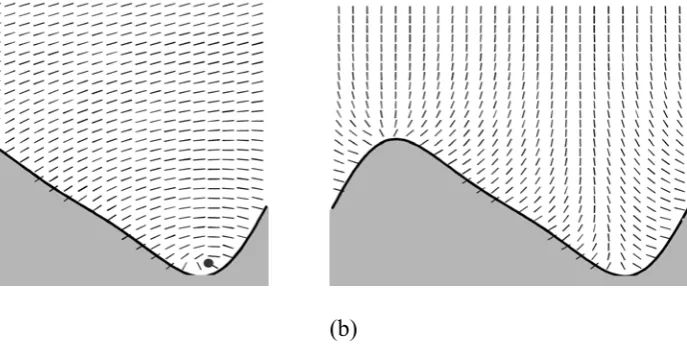
The liquid crystal director field near to the surface for the two bistable states is represented in figure 1. The high director tilt state has no defects and is termed the continuous or C state; the low director tilt state has + ½ and – ½ strength defects at
the surface troughs and peaks respectively and is termed the defect state or D state.
Within a short distance from the surface (typically less than the pitch of the grating) the director field approaches a uniform state. For a local homeotropic surface condition, the C state is near vertical (high surface pre-tilt), whereas the D state has a
lower surface pre-tilt. Each stable state may have different optical properties. For example, when assembled as part of a normally white twisted nematic cell, the D state
appears light and the C state dark. The devices respond to an electric field in the
conventional way for a nematic liquid crystal. However, they also have a polar latching response [1, 4] where pulses of appropriate polarity and above some threshold time and voltage product may induce a transition from one state to the other. Latching occurs from C to D for a positive field with respect to the grating surface
ordo-electric and flexo-electric terms induced in the liquid crystal by the deformation close to the grating. It has been theoretically confirmed [7, 8, 9, 10] that the flexoelectric properties of the liquid crystal allow it to respond to the sign of an applied electrical signal, thus providing a means to electrically select either bistable state. In practice, bipolar electrical pulses are used to reduce the effects of ions within the liquid crystal during switching [11] and also serve to keep defect nucleation and annihilation as surface phenomena. The trailing edge of the bipolar pulse selects the latched state.
The ZBD surface is a two dimensional periodic grating structure that includes
phase shifts in the grating so as to yield good operating performance [5, 4]. These phase shift interface regions, or slips, provide vertical concave and convex surfaces periodically along the length of each grating groove. These slips help stabilise the +/- ½ strength disclinations of the D state into a three dimensional defect loop structure,
serving both as a pinning and annihilation site. However, when both the phase shift distance is large and the onset of defect nucleation/annihilation is mid channel, the threshold fields for latching can be considered theoretically as a two dimensional problem.
An analytic solution to the behaviour of the ZBD is difficult to obtain because of the complexity of the governing partial differential equations and the imposed boundary and switching conditions. Reductions to one dimensional models [12, 13] with fictitious surface potentials seem too simplified to capture the operation of a real ZBD and, hence, cannot be relied upon for engineering improved surface designs and devices. The equilibrium states of the ZBD device, using the Frank free energy, have been studied numerically by Bryan-Brown et al. [1] and Brown et al. [14]. Denniston
material. In [10], the authors studied the defect trajectories in the presence of a non degenerate surface shape and also studied the defect annihilation times with changing material parameters. However, [10] only considered the D to C transition, using
monopolar pulses.
In the current work we aim to establish not only a qualitative but a semi quantitative comparison between modelling and experiment. Following the methodology set out in [10], modelling is carried out to determine the threshold latching voltages for specific surface designs and real liquid crystal materials. These values are readily verifiable by experiment and, thus, may be considered as a confirmation of the correct dynamics of defect nucleation and annihilation. The ZBD LCD is possibly one of the most complex of all commercialised LC devices; it necessitates the use of at least two dimensional modelling, must include order parameter variations and extremely fine length scales (because defects are microscopic) and must use flexoelectricity. This article is the first time both experiment and theory of the ZBD devices have been quantitatively combined. The following section recalls the necessary theory and numerical method used in this work. Section III contains experimental detail on the manufacture of the ZBD surface and latching measurements. Section IV then details the results and makes comparisons with experiment and is followed by a brief conclusion section.
II. THEORY
The presence of defects in a ZBD imposes a microscopic length scale and necessitates the use of numerically intensive but standard liquid crystalline theory. We apply the Landau de Gennes theory [15, 16] based on an alignment tensor field, Q. The governing dynamic equations for Q are presented, for example, in [10] along with a method of solution used in this work. The phenomenological free energy of the liquid crystal device and ZBD surface is defined as
(1)
,
V FLdG Felastic Felectric Fflexo dV S Fsurface dS
F
where
(2)
, 2
1
0 QQ QQQ QQQQ F
(3)
(4)
(5)
(6)
where ( )
3
4 *
T T a
F
, F B
3 4
, F C
9 4
are thermotropic coefficients of the
material, x
, Li,i14are elastic constants, 0is the permittivity of free
space, the liquid crystal dielectric tensor, is the maximal dielectric
anisotropy (given by the difference of the principal components),
max
a
1
and 2 are
flexoelectric coefficients and the Einstein summation convention is used for the
Cartesian coordinates. E is the electric field and W the homeotropic anchoring
strength in the preferred order Q0. In the limit of constant order parameter, this form of the free energy maps directly into the Frank free energy based upon the director,
.
The material coefficients for the Frank description are more widely known.
The Landau de Gennes theory is a small Q expansion [15, 16] initially
proposed to study pre-transitional and critical phenomena at the isotropic nematic transition. The validity of the expansion deep in the nematic phase, where the order parameter S is no longer <<1, is less clear. It has been shown by Qian and Sheng [17] that this method quantitatively maps onto the dynamics of the Ericksen-Leslie-Parody theory [18] in a simple twisted nematic cell arrangement. Quantitative studies of the Landau De Gennes method to cases in which defects are created, annihilated and move in the nematic phase are less common in the literature but it is shown here that it can still be used with confidence.
Here, the free energy Eq. (1) is solved by the lattice Boltzmann (lB) method of Spencer and Care [10]. The device domain is modelled on a regular sized grid over one surface grating period. The constant grid size increases the computational
2 1 2 1 2 1 2 1 4 3 2
1 Q Q L Q Q L Q Q L Q Q Q L
Felastic ,
, 6 1 3 1 2 0 max
0 E Q E E
Felectric a
, 2
1
E Q E Q Q
Fflexo
. 2 2 0 Q Q
W
demands of the method. This is because the same grid that is used to resolve the defect order structure at the surfaces is used throughout the non defect areas of the cell. However, it also leads to a good representation of the surface curvature. The use of the lB method in comparison to finite differences provides increased stability to the numerically stiff equations, reduced numerical dispersion and is still readily parallelisable. The hydrodynamic backflow effects are not calculated for the results presented. It is anticipated that the backflow effects will contribute minor quantitative corrections to the results due to the high non-slip surface area. The cell is modelled as a two dimensional cross section of the mid slip region yet retains three dimensional orientation.
A ZBD surface is computed from scanning electron microscope (SEM) images of the surface in question. This is then digitised and a cubic spline fit undertaken, with a ±5nm confidence level, from which the surface location and unit normal vectors are
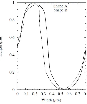
interpolated in the lB domain. Typical surfaces are shown in figure 6. The ZBD
surface is assumed to have finite homeotropic anchoring W, and the opposing flat
surface is assumed to have infinite anchoring with polar and azimuthal angles of 86
and 94 degrees (in accordance with the grating asymmetry) giving a
twisted nematic arrangement. Symmetric bipolar square wave latching voltages are computed by setting the voltage pulse lengths, , then employing a binary search method to identify the threshold voltage, V . The pulse length of each polar field is
equal to .
In order to determine the instantaneous electric field distribution, Maxwell’s equations are solved using a successive over relaxation method [10] and also applying a Gauss’s law via a trapezium integration directly to the grid points on the boundary between ZBD surface and liquid crystal medium. This latter step is required in order to accommodate the large discontinuity in the dielectric permittivity between the ZBD surface material and the liquid crystal in use. Dirichlet boundary conditions on the voltage are applied at the upper surface (zd ) and lower (z 0) electrode surfaces.
III EXPERIMENTAL
The ZBD uses a nano-replication method to pattern the LCD mother-glass with the grating shape, similar to the method used in CD/DVD fabrication [4]. The first step is to define the pre-requisite pitch, mark-to-space ratio, slip periodicity and structure into a chrome on glass mask. This is done using a dry etch method common to the industry for the production of photolithographic masks for silicon wafer fabrication. The mask is then used to selectively expose ultra violet (UV) light into a photoresist layer spin coated onto a glass substrate. A broad range of grating shapes can be made by varying the chrome pattern and the process conditions (such as exposure angle and bake temperatures). The resist pattern is then converted to a family of nickel tooling shims using a combination of sputtering and electro-forming methods. The nickel is used to form the shape in a suitable resin deposited onto a flexible film. This film in turn is employed as an embossing tool in the LCD fabrication steps. The grating shape is transferred from the film to the patterned indium tin oxide (ITO) coated LCD glass by embossing into a UV curable photo polymer that is either chosen to give the correct homeotropic alignment state to the contacting nematic liquid crystal, or is subsequently coated with a homeotropic surfactant. The final LCD grating shape, therefore, is defined by the original photo-resist master plus the degree of shape change through the nickel, film and embossing processes. For the cells used in the current study, a simple acrylate photopolymer was used for the grating material, and homeotropic alignment was induced by coating with trichloro-alkyl silane deposited in the vapour phase under conditions of controlled humidity [19]. The anchoring properties of the surface were controlled by varying the exposure to the silane vapour to control the density of the surfactant on the surface. Accurate control of the anchoring was possible by monitoring the liberated hydrogen chloride (HCl) vapour from the silane polymerisation reaction in the presence of the water using a sensor from City Technology.
The first nickel tool (called the father) faithfully reproduces the original photo-resist master. Additional nickel tools (mothers), derived from the father, undergo a small (~1 nm in width) dimensional change for each successive mother growth. This
(through both UV and thermal processing). The overall shape change from master to final LC device is about 10% in both grating depth and width.
The grating coated substrate is spaced from a standard rubbed polyimide counter plate using glass bead spacers. The direction of the rubbing is coincident with the grating groove direction so that a 90° twist of the director results when the D state
is formed. A thermal glue seal is used to hold the plates together and nematic liquid crystal introduced under vacuum through capillary forces. Throughout this work, Mixture B from [11] was used, together with Nissan SE3510 as the polyimide on the opposing monostable surface. The Gooch Tarry first minimum for this liquid crystal is for a 5 micron cell gap, though devices of different spacing are used for the experimental work. Before studying, the device is annealed briefly in the isotropic phase. The D state is then formed uniformly over the whole device on first cooling
since this is the state preferred at high temperatures where the nematic order parameter is low and disclinations energetically favoured at the top and bottom of the grooves. This is particularly useful for practical devices because it ensures that areas of a display not subject to electrical field, such as the boundaries and inter-pixel gap regions, are in a single uniform D state.
The electrical latching of the device is achieved by applying appropriate pulse trains generated using a Wavetek 100 MHz synthesized arbitrary waveform generator
(model 395) in conjunction with a x10 amplifier. The Wavetek allows the pulse width
() and height (V) to be selected ( is 500 microseconds unless otherwise stated).
The preferred method of latching to the C or D states selectively [20] is to use bipolar
pulses, with the resultant state being dictated by selecting the polarity of the bipolar pulse. Experimentally, uni-directional latching from the D to the C state only can also
be induced using a high-frequency pulse train of sufficient magnitude [11]. Categorisation of latched states is achieved by observation through an Olympus microscope using polarised illumination in transmission, with a crossed analyser and polarizer.
Close to the clearing temperature the device becomes D state monostable. The
temperature of the spontaneous transition from C to D was measured by first latching
into the C state, and then observing the onset of D state formation whilst slowly
IV. COMPARISON OF MODELLING AND EXPERIMENT.
In this section, we compare the threshold latching fields in the ZBD determined from the modelling and experiment. The agreement between experimental and modelling method validate the modelling approach which has been adopted.
The material parameters used throughout this work are chosen to closely match the real system: K11 = 12.5 pN, K22 = 7.3 pN, K33 = 17.9 pN, K24 = 3.0 pN, 1 =
0.155 kg m-1 s-1, LC = 62.5, = 39.0, surface = 13.5, e11 = 69 pC m-1, e33 = 45 pC
m-1, lS = 0.2m, a = 65000 J m-3 K-1, B = 530000 J m-3, C = 980000 J m-3, equilibrium
temperature S = S0 = 0.49. We note the chosen liquid crystal material has a large
dielectric anisotropy which increases the electric field line diffraction particularly at the ZBD surface [11]. Measurements of the elastic and dielectric constants, and the
value for the viscosity 1 (predicted using measurements from the individual mixture
components) were made by Francis and Goulding from E. Merck [11]. The flexoelectric coefficients of the liquid crystal were obtained from [21], where an experimental uncertainty for the magnitude of e11+e33 was given as 50%. For
simplicity, the anchoring energy of the mono-stable polyimide surface is assumed to be infinite.
There are few available measurements of the Landau values for liquid crystal mixtures; here, we use values measured by Coles [22] for 5CB. Deviations from these values change the length scale of the theory. For example using values an order of magnitude smaller will increase the defect sizes and allow unrealistically large order parameter variations: in terms of ZBD device latching the threshold voltages would be reduced. We use the measured values of the flexoelectric coefficients in all results presented, however, we note, from a material design point of view, in numerically exploring the phase space of both flexoelectric coefficients with respect to V latching low voltages may be obtained when e11>0 and e33<-e11. This agrees with the findings made by Parry-Jones et al. [9] who considered bulk flexoelectric effects in the
absence of dielectric anisotropy.
grating shape, and the magnitude, frequency and time of the applied electric field. When deviating from typical device operating conditions the defect nucleation annihilation dynamics can be quite varied and complex.
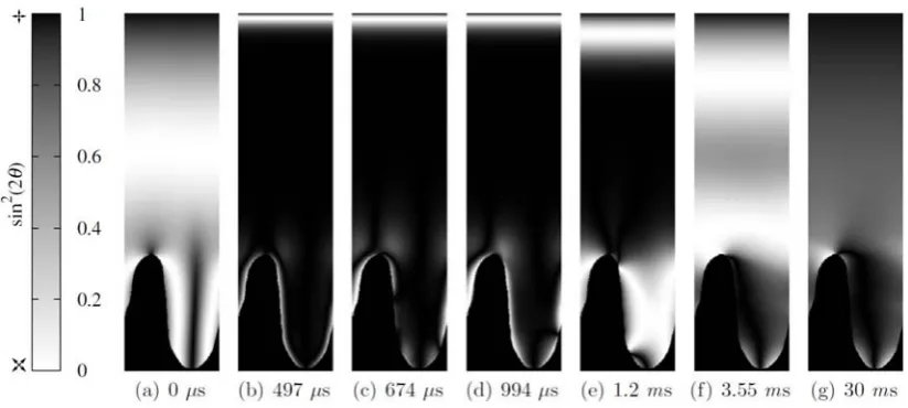
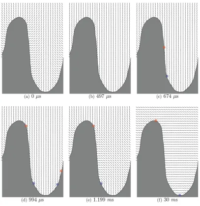
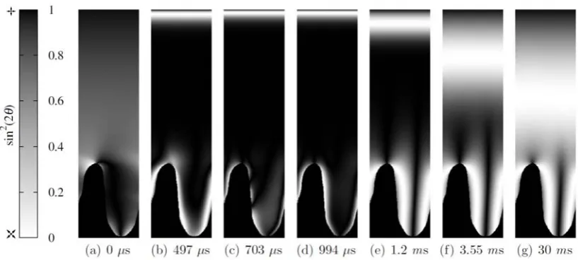
We show selected simulations from typically used parameters close to typical operating conditions in figures 2 to 5. The figures represent two-dimensional cross sections of a 3 m spaced twisted nematic cell for ZBD surface shape A (see figure 6)
and an applied bipolar voltage pulse 1 volt above the V latching threshold with =
500s. Figures 2 and 4 represent the director polar angle projected onto the image plane during the latching process and figures 3 and 5 are schematics of the defect and director structure in the vicinity of the ZBD surface.
The evolution of the C to D transition is summarised in figures 2 and 3. The
liquid crystal has a strong positive dielectric anisotropy and the grating material has a relatively low permittivity leading to strong electric field refraction in regions of high surface curvature. The bulk director field aligns with the applied electric field confining director distortions to the surface and the flexoelectric effect, which is always stronger at surfaces than in the liquid crystal bulk, couples to the first portion of the applied electric field (i.e. the first slot of the bipolar pulse where the field is negative) to enhance the continuous state and raise the order parameter at the surface,
figure 3(b). The second (positive) portion of the electric field coupled to the flexoelectric effect then gives rise to a lower order parameter and is used to nucleate a defect pair at the grating sidewall at approximately half height, figure 3(c). These defects then move to areas of favoured curvature and a second defect pair nucleates on the other, less banked, grating sidewall, figure 3(d). Removal of the applied field sees the defects in close proximity annihilate under attractive forces but the original defect pair remains and migrate to their regions of favoured strong curvature thus forming the D state.
Using a V value exactly on the C to D latching threshold usually results in a
is independent of this process. After the electric field is removed, the director in the bulk of the sample re-orients to form the TN state over a time dictated by the viscoelastic properties of the liquid crystal.
The evolution of the D to C transition is summarised in figures 4 and 5. The
-½ defect favours the convex surface curvature at the groove top, whereas the +-½ defect favours the concave curvature of the groove bottom. The first (positive) portion of electric field coupled to the flexoelectric effect near the ZBD surface gives rise to a lower surface order parameter and pins the defects in place whilst the bulk director field aligns to the applied electric field direction. This bulk alignment keeps the director distortions close to the ZBD surface. The second (negative) portion of the electric field coupled to the flexoelectric effect then raises the order parameter and caused a torque that pushes the defects along the grating sidewall to annihilate. Turning off the applied field in this defect-free state allows the cell to elastically relax into the hybrid-aligned nematic C state. In this case, the optical response is much
faster than after the C to D transition, since the director in the bulk of the sample is
already substantially re-oriented in response to the applied field.
Using a V value at the D to C latching threshold usually results, when the
field is turned off, in a similar state to figure 4(c) in which a defect pair remain on the grating side wall but they have sufficient proximity that the opposite strength defect
attractive force will cause defect annihilation. Reducing the V value below this threshold will usually result, when the field is turned off, in a similar state to figure 4(b) in which case the defect pair do not have sufficient proximity and the D state
remains. An example of defects moving away from the surface using monopolar pulses with a smaller grating height maybe found in Spencer and Care [10].
The modelling has been used to investigate several dependences of ZBD behaviour, as outlined in the following sections.
A) Cell gap and anchoring energy measurement
It has been observed in actual zenithal bistable liquid crystal devices that the threshold field varies linearly with cell gap [11]. We model this behaviour for a ZBD cell finding the C and D state equilibrium conditions for a range of cell gaps from m each using surface profile A, shown in figure 6, but with different 5
homeotropic anchoring strengths W. The binary search method is then used to
identify the latching voltages at each cell gap and anchoring energy.
The results obtained from the model are shown in figure 7 for the C to D
transition with =500 s. A linear dependence of the latching threshold VCD with cell
gap is seen. It is also found that the gradient of this linear behaviour depends upon the homeotropic anchoring strength. Lower latching voltage are seen at smaller anchoring strengths. The behaviour is approximately given by:
W d
VCD , (7)
with the best fit for the parameters given by = 7.4 x 10⁹ C-1 m and = 2.1 x 10⁻¹⁰ m.
Davidson and Mottram [13] used a one dimensional approximation to a ZBD driven by the flexoelectric torque and found an analytical solution for the static critical threshold field Eth below which latching from C to D would not occur, as
given by:
d E K K E W e e th a ath
0 0 33 11 tanh 8
. (8)
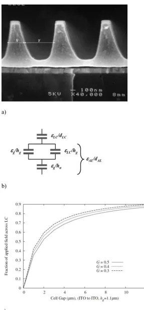
Following the analysis of Jones et al. [11], the electric field for a rectangular grating
can be approximated by the simple capacitive circuit shown in figure 8. The electric field applied across the liquid crystal in the grating aligned cell is then:
LC LC g g g u LC LC G G h h d V E ) 1 (
, (9)
where G is the grating shape factor G = X/(X+Y) corresponding to the full width half
maximum / grating pitch, X and Y are the grating ridge width and corresponding
groove width, respectively, hg is the height of the grating, hu is the combined height of
hu. With a bipolar pulse train, the first of the two pulses couples to the strong positive a to induce near vertical alignment in the bulk of the cell. In this case, the permittivity of the liquid crystal LC approaches ||. Typically, 0.3 < G < 0.5 and 4m
< d < 10m, hence between 60% and 90% of the field is applied across the liquid crystal. Reference [4] includes a typical measurement for the temperature dependence of the static minimum threshold voltage calculated by extrapolating the latching time. This is also discussed in section C of the current work. Applying Eq. (9) we estimate that Eth > 0.5V/m close to the upper monostable transition temperature, and is
typically Eth ≈ 2V/m. Given the following practical ranges for the elastic constants
and the dielectric anisotropy 5 pN < Kii < 20 pN ; +10 < < 40 then the tanh term of
Eq. (8) tends to unity. Substituting for the applied field using Eq. (9) yields:
Y X X h h d K e e W d Y X Y X h h K e e W V g g g g u LC g g g u th || || || 33 0 33 11 || || 33 0 33 11 || 1 ) ( 2 ) ( ) ( 2 , (10)
where K is assumed to be given by K33 for bipolar pulses because the latching occurs
when the bulk of the sample is aligned vertically. This key equation identifies a route to lowering operating voltages via material selection (high e11+e33, a and K33 liquid
crystals and low W surfaces), though it does not contain detailed information on ZBD
surface shape optimisation. The surface shape terms contained in Eq. (10) merely indicate the 1-dimensional drop in applied field caused by the dielectric effect of the grating and do not represent the in-plane electric field terms or the effect of surface curvature that will strongly influence defect annihilation, creation and dynamics in the
actual device. We also note that if 2 and
S
W e11,e33 S then which has
been shown experimentally by Jones [4]. Comparing this analytical approximation with the numerical results summarised in Eq. (7) gives:
S Vth
33 0 33 11 ) ( 2 K e
e a
Y X X h h g g g g u || || || 1 ,which have the values = 1.0 × 10¹⁰ C-1 m and = 6.5 x 10⁻⁷ m for the parameters
used in the model (with X = 320nm, Y = 480nm, hg = 1.0m and hu = 80nm). This
analytical estimate for is to within 25% of that determined by the numerical
simulation. The large discrepancy between the analytical and that obtained by the numerical simulation is mainly because of the one dimensional analytic approximation (particular the dielectric behaviour) in a two dimensional geometry, and also because of the time dependence included in the numerical data that simulates
the response to =500s pulses, whereas the analytical expression simulates the static field limit. Importantly, this analysis shows that the gradient of the VCD transition
versus cell gap is a measure of the homeotropic anchoring energy, regardless of the pulse width used in the experiment.
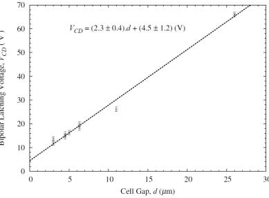
The theoretical C to D latching voltages shown in figure 7 compare well to the
experiment values of figure 9. Experimentally, the cell gap d is controlled precisely
using appropriately sized glass spacer beads. The anchoring energy is kept constant by using the same homeotropic polymer, process parameters, and the same grating shape in each cell. Experiment shows a linear dependence for the C to D latching
voltage with cell gap, with a positive intercept 3.5±1 V and gradient of 2.5 ±0.2 V/µm. The anchoring energy can be estimated for these experiments by comparing
the gradient VCD versus cell gap, which is related to W / (e11+e33), to the modelling
results. From this we obtain a zenithal anchoring energy W of (2.8 ± 1) × 10-4 J m-2
for the system studied in figure 9. Note, it was not possible to fit the experimental data directly using the computer model because of the computational expense and time that this would involve.
Literature measurements of homeotropic anchoring energies for positive nematics are relatively rare, due to the experimental difficulty of providing a sufficiently strong deforming field with a component normal to the homeotropic
condition. For example a value of W = (5 ± 1) × 10-5 J m-2 for the nematic 5CB on a
strong homeotropic anchoring that is required for the zenithal bistable device, as
described in the following section. Other literature measurements of W for a
homeotropic surface have been made with dielectrically negative nematic materials. For example, reference [24] obtains (4.6 ± 0.2) × 10–4 J m–2 for a surface coated with the surfactant lecithin, which is similar to the value obtained in the current work.
Figure 10 shows the change in the static threshold voltage theoretically predicted by the one dimensional analytical expression in Eq. (10) with different grating shapes and a fixed anchoring energy of W = 2.85 × 10⁻⁴ J m-2. Also indicated
are the expected values for the grating shapes A and B from figure 6.
B) Homeotropic anchoring strength
Using a constant cell gap d = 2 m and shape A the latching voltages for the C
to D and the D to C transitions are numerically calculated for a range of
experimentally achievable values of the homeotropic anchoring strength,
J m-2. The results at = 500 s are shown in figures 11(a) and
11(b). A higher homeotropic anchoring strength requires a larger magnitude of latching voltage in both D to C and C to D transitions, a relation that is seen to be
nearly linear, as expected from Eq. (10), over the range of typical homeotropic
anchoring strengths used. We note that below an anchoring strength of J
m-2, although both C and D states can be obtained, the latching is always monostable
in the C state. This indicates that a finite W is required to stabilise the defect
nucleation.
3 4 1 10
10
1
W
4
10
1
W
In practise the anchoring energy can be varied by changing the density and/or strength of aligning groups at the grating surface. There are several methods by which this can be achieved. For example, a surfactant can be deposited onto the grating surface, the density of which can be varied by controlling the dilution or contact time with the surface. Such changes can be monitored by measuring the contact angle of reference liquids (typically mono-bromo naphthalene, di-iodo methane and de-ionized water) on a flat witness sample of the homeotropic grating surface [25]. Figure 12 shows the latching voltages for a series of 5.25µm spaced cells in which the surface
approximate linear dependence between surface anchoring energy W and surface
energy is assumed. This is supported by the comparison of the modelling and experimental results. For the grating shape used in this experiment, figure 6, VDC / VCD
= -0.92, which is similar to the theoretical value of -0.75 shown in figure 11, again suggesting a good qualitative match between theory and experiment. Comparison of the results of figure 12 with the modelling work from the previous section suggests that control of the surfactant density leads to anchoring energies ranging from 8 × 10⁻⁵ J m-2 ≤ W ≤ 4 × 10⁻⁴ J m-2. In practice, attempting to coat the grating surface with
higher surfactant densities led to patchy alignment. This is assumed to be due to the saturation above the formation of the first monolayer [19]. The ability to vary the latching voltage by chemical means is attractive from a manufacturing perspective since it allows precise control over variations in grating shape (e.g. small differences from different batches of masters or changes in process giving rise to changes in shape).
Figure 12 also shows the variation of monostable transition temperature and
twist off angle t with varying surfactant density. The latter measurement is the angular deviation of the in-plane component of the director from the expected orientation normal to the grating grooves and surface. Experiments show that low
surfactant densities for which W < 1 × 10⁻⁴ J m-2 lead to twist of the director in the D
state close to the grating surface as the director is forced towards the grooves. At sufficiently low concentrations, the zenithal anchoring energy is too weak to prevent the director from being forced to lie parallel to the grating grooves. For anchoring below 8×10⁻⁵ J m-2 the cell will still cool into the D state, and latches into the C state
after application of an appropriate electric pulse, but it will not latch back into the D
state and the device is mono-stable. The numerical modelling has replicated the behaviour found experimentally.
C) V response curve and grating shape
The latching voltage is known to depend upon the duration of the applied voltage pulse, . In figure 13 we plot results from the model’s V response for the
to D and the D to C transitions have comparable voltage magnitudes. At longer pulse
lengths the C to D transition requires voltages of larger magnitude. These are
qualitatively consistent with the empirical findings of Jones [4]. Figure 13 also contains a comparison between the behaviour of the two different shaped surfaces A and B. In each case the numerical data was satisfactorily approximated by the simple expression: ) )( ( . , 33 11 , 1 i th i i S i V V e e d l
; i = CD, DC. (12)
Note, the form of [12] differs from the empirical fits used in [4] because of the effect of ions on the latching. The best fits use the surface viscosity coefficients ls,CD = 0.06 m and ls,DC = 0.09m independently of the grating shape. The minimum voltages
below which latching cannot be induced regardless of pulse duration were dependent of the grating shape, with Vth,CD = 9.9V and Vth,DC = -6.4V for grating shape A, and
Vth,CD = 11.6V and Vth,DC = -7.1V for grating B, respectively. Again, applying Eq. (10)
allows the homeotropic anchoring energy to be determined from the C to D static
threshold voltages: shape A corresponds to W = 2.3 × 10⁻⁴ J m-2 and shape B to W =
2.7 × 10⁻⁴ J m-2. These values are both within the experimental error determined from the cell gap dependence. However, it should be noted that the differences in threshold are larger and of the opposite sign to those predicted by Eq. (10) (see figure 10). The reason for this physical difference is discussed below.
There are two important contributions to the minimum voltages relating to grating shape design, and causing shape A to exhibit lower minimum voltages than shape B. These are the effect of the dielectric mis-match between the liquid crystal and the grating, and the effect of the surface curvature on the near-surface ±½ disclinations. The relative importance of these effects differs for each of the transitions, from D to C and from C to D. Consider the D to C transition. It is
annihilate. Reducing high curvature regions will, thus, lower the D to C transition
threshold (i.e. make the latching voltage less negative).
In the C to D transition, shape A has a lower latching threshold than shape B.
It is suggested that the reason for this is the increased ‘width’ of the surface peaks that contain low permittivity material. This increases the dielectric response at the surface, enhancing the lateral components of the electric field and so promoting the nucleation of the defects. Increasing the width of the dielectric features can, thus, lower the C to
D transition threshold. A measure of this width can be obtained from the ZBD surface
full width half maximum (FWHM). This has been demonstrated in figure 14 in which the experimental =500s VCD threshold is plotted as a function of grating FWHM.
[image:20.595.129.505.679.745.2]The grating FWHM in this case is varied by deriving the grating shape from successive nickel mother shims. Direct SEM measurements of the grating structures in cross section allows accurate determination of the grating width.
Figure 15 shows the experimental V curves for two further grating shapes
and obtained from different nickel mothers from Shapes A and B [26] and
constructed using a surface with an anchoring energy W = 7 x 10⁻⁴ J m-2. These have
a grating depth of 1 micron and FWHM/pitch = 0.462 and FWHM / pitch = 0.398, respectively. Unlike the measurements of reference [4], these samples were prepared using precautions to avoid ionic contamination (such as the use of commercial grade liquid crystal and glue seal materials). The fits deviate from Eq. (12) at short time slots due to losses caused by the series electrical resistance to the cell. However, at longer times and lower voltages the experimental data compare well with the modelling results shown in figure 13, both in form and magnitude, further validating the accuracy of the model. The fit parameters are given in table I. As noted earlier for the numerical result, the experimental V curve also shows a decrease in threshold for increasing G.
In summary, Eq. (10) and Eq. (12) may be combined to predict the bi-polar latching behaviour of the zenithal bistable device:
Y X X h h d K e e W e e d l V g g g g u a i i s i || || || 33 0 33 11 33 11 , 1 1 ) ( 2 ) ( . ;The surface viscosity ls is shape dependent, i.e. ls = f(X, Y). This dependence will be considered in further work.
Table I Summary of the fitting parameters for the V curves to Eq. (12)
DC transition CD transition
Result G =
FWHM/P ls,DC (m) Vth,DC (V) ls,CD (m) Vth,CD (V)
Theory A 0.435 0.09 -6.4 0.06 9.9
Theory B 0.36 0.09 -7.1 0.06 11.6
Experiment 0.462 0.46 -8.5 0.18 5.9
Experiment 0.398 0.59 -9.5 0.29 8.9
D) Investigation of the grating pitch
We now give a further example of the role that surface shape has upon the device response by varying the pitch of the ZBD surface. We consider shape A, characterised by an amplitude h and pitch w. In this we vary the pitch whilst
maintaining the surface profile and keeping the ratio h/w constant. The cell gap is
fixed at d = 3m and the anchoring strength J m-2. The equilibrium
states and V responses from the model at various pitch values,
4
10 3 .
3
W
5 . 1 5
.
0 w m, are
shown in figures 16 and 17 respectively. These show that a larger pitch gives rise to greater latching thresholds for all values of . Figure 17 plots the calculated latching voltage response as a function of pitch. The thresholds follow a near linear dependence on pitch.
V. CONCLUSION
A direct comparison between theoretical approximation, a detailed numerical model and experimental behaviour in the ZBD liquid crystal display has been undertaken for the first time; the results show excellent agreement. This correspondence between numerical modelling and experiment confirms the applicability of the Qian and Sheng approach to solving the Landau De Gennes theory for liquid crystals in the presence of defect nucleation and annihilation processes, and that only by including a full set of realistic material and two dimensional surface parameters can the qualitative device properties be recovered within a modelling framework. The numerical results and the analytical approximation together provide clear insight into the ZBD latching mechanism and dynamics. In addition, the theoretical approximations highlight a route to optimise latching thresholds through appropriate material selection and are also applicable to a device in which a three dimensional surface structure may be used.
A measurement of the homeotropic anchoring energy has been undertaken by comparing the voltage response in a ZBD as a function of cell gap; we find the homeotropic anchoring energies can be varied in the range 0.5 to 4 x10⁻⁴ J m-2. The relationship between surface homeotropic anchoring energy and latching thresholds has been shown. The influence of several key surface shape parameters has been explored, indicating routes to further reducing the latching voltages in a ZBD device. The good correlation between simulation and experiment shown here indicate that further theoretical explorations of the surface shape should yield reductions in the latching voltages required.
ACKNOWLEDGEMENTS
REFERENCES
[1] G. P. Bryan-Brown, C.V. Brown and J.C. Jones, U.S. Patent 6249332, (1995).
[2] G.P. Bryan-Brown, C.V. Brown, J.C. Jones, E.L. Wood, I.C. Sage, P. Brett and J.
Rudin (1997) SID Symposium Digest, 28, pp37-40, (1997).
[3] J.C. Jones, S.M. Beldon and E.L. Wood, J. SID., 11, 2 pp 269 – 275 (2003).
[4] J. C. Jones, Journal of SID, 16, 1, pp143 – 154 (2008).
[5] J. C. Jones Patent Application WO 2004 / 070465 A1 (2003).
[6] E.L. Wood, V.C. Hui, G.P. Bryan Brown, C.V. Brown and J.C. Jones, US Patent
7053975, (2000).
[7] C. Denniston and J. M .Yeomans, Phys. Rev. Lett. 87, 275505 (2001).
[8] L. A. Parry-Jones and S. J. Elston, J. Appl. Phys. 97, 093515 (2005).
[9] L.A. Parry-Jones, R.B. Meyer and S. J. Elston, J. Appl. Phys., 106, 014510
(2009).
[10] T.J. Spencer and C.M. Care, Phys. Rev. E, 74, 061708 (2006).
[11] J. C. Jones, S. Beldon, P. Brett, M. Francis, and M. Goulding, SID Symposium
Digest, 34, 945 (2003).
[12] F. P. DA. Costa, M.Grinfeld, N. J. Mottram and J. T. Pinto, Mathematical
Models and Methods in Applied Sciences, V17, n12, p2009 (2007).
[13] A. J. Davidson, and N. J. Mottram, Phys. Rev. E, 65, 051710 (2002).
[14] C. V. Brown, M. J. Towler, V. C. Hui and G. P. Bryan-Brown. Liq. Cryst. 27,
233 (2001).
[15] P.G. De Gennes, Phys. Lett. 30A, 454 (1969).
[16] P. G. De Gennes, Mol. Cryst. Liq. Crsyt. 12, 193 (1971).
[18] P. G. De Gennes and J. Prost, The Physics of Liquid Crystals (Clarendon Press,
Oxford, 1993).
[19] J.C. Jones and G. P. Bryan-Brown, unpublished .
[20] J.R. Hughes and J.C. Jones, US Patent US6,784,968 (1999).
[21] C. Kischka, S. J. Elston and E.P. Raynes, Mol. Cryst. Liq. Cryst. 494, pp
93-100 (2008).
[22] H.J. Coles, Mol. Cryst. Liq. Crystl. 49, 67 (1978).
[23] L. M. Blinov and A. A.Sonin, Sov. Phys. Tech. Lett., 14 (7) pp510 – 511
(1989).
[24] F. Yang, L. Ruan and J. R. Sambles, J. Appl. Phys. 88, 6175 (2000).
[25] J. C. Jones, SID Symposium Digest, 37, 2, pp 1626–1629 (2006).
[26] R. M. Amos and J. C. Jones, SID Symposium Digest 40, 3, P120, pp 1577 –
FIGURES
[image:25.595.141.485.267.442.2]
(a) (b)
Figure 1. Schematic of the director profiles of the liquid crystal in the vicinity of the ZBD surface over a one pitch variation. (a) the defect state, D (b) the continuous state,
Figure 2. Typical representation of C to D latching dynamics in a ZBD cell at a
voltage 1 volt above the latching threshold and = 500 s, where t = 0 corresponds to
the initial application of the bi-polar pulse, t = 500s corresponds to the reversal of the field half way through the bipolar pulse and the electric field is removed at t = 1ms. Shown is the director polar angle only; there is also a ~/4 twist in the
Figure 3. Schematic, at the ZBD surface, of the C to D transition involving nucleation
Figure 4. Typical representation of D to C latching dynamics in a ZBD cell at a
voltage 1 volt above the latching threshold and = 500 s, where t = 0 corresponds to
the initial application of the bi-polar pulse, t = 500s corresponds to the reversal of the field half way through the bipolar pulse and the electric field is removed at t = 1ms. Shown is the director polar angle only; there is also a ~/4 twist in the
Figure 5. Schematic, at the ZBD surface, of the D to C transition involving defect
Figure 7. Modelling results showing the linear behaviour of the C to D transition for
pulse length = 500 s as a function of cell gap, for a range of homeotropic
a)
b)
[image:32.595.87.375.63.682.2]c)
Figure 8. Approximation for the electric field across a grating aligned LCD. a) Definition of FWHM = X and pitch = X+Y; b) equivalent circuit for grating; c) E field
Figure 9. Experimental behaviour of the C to D transition, at pulse length = 500 s
Figure 10. Predicted dependence of the static threshold voltage for the C to D
transition as a function of grating shape G = X / X+Y from the one dimensional
(a)
[image:35.595.91.462.63.659.2](b)
Figure 11. Modelling results showing variation of latching voltage, = 500 s, as a
(a)
[image:36.595.89.446.77.631.2](b)
Figure 12. Experimental results for (a) the 500s latching voltages (VCD and VDC) for
5.25m spaced ZBD cells and (b) the monostable transition temperature and the D
state surface twist-off angle t as a function of the surfactant density (indicated by the
(a)
[image:37.595.90.434.77.637.2](b)
Figure 13. Modelling results showing V curve for the ZBD surfaces shape A (solid
points and continuous line) and shape B (open points and dashed line) given in figure
6. The lines are the best fits to Eq. (12). Figure a) shows the C to D transition, and b)
Figure 14. Experimentally measured C to D latching voltage, = 500 s and cell gap
Figure 15. Experimentally measured V curves for gratings of depth 1 micron for
shape (FWHM/pitch G = 0.462, closed points and continuous line) and shape
(a)
[image:40.595.91.497.73.674.2](b)
Figure 16. Plots of the director polar angle in the equilibrium states (a) C, and (b) D
for shape A considered at different pitches and constant h/w. Note there is a /4
Figure 17. Modelling results showing the V response of a ZBD cell of shape A
Figure 18. Experimental V curves for ZBD cells made with gratings of pitch w = 0.8