SEMICONDUCTOR TECHNICAL DATA
QUAD MDTL LINE DRIVER
EIA–232D
PIN CONNECTIONS
P SUFFIX PLASTIC PACKAGE
CASE 646
D SUFFIX PLASTIC PACKAGE
CASE 751A (SO–14)
2
Output C Input C2 Input C1 Output D Input D2 VCC 14
Input D1 VEE
Input A
Output A
Input B1
Input B2
Gnd Output B
8 9 10 11 12 13
7 5 3
4 1
6
The MC1488 is a monolithic quad line driver designed to interface data terminal equipment with data communications equipment in conformance with the specifications of EIA Standard No. EIA–232D.
Features:
•
Current Limited Output±10 mA typical
•
Power–Off Source Impedance 300 Ω mininum•
Simple Slew Rate Control with External Capacitor•
Flexible Operating Supply Range•
Compatible with All Motorola MDTL and MTTL Logic FamiliesORDERING INFORMATION
Device
Operating
Temperature Range Package
MC1488P
TA = 0 to + 75°C Plastic
MC1488D TA = 0 to + 75°C SO–14
Circuit Schematic
(1/4 of Circuit Shown)
GND 7
3.6 k Pins 4, 9, 12 or 2
Input Pins 5, 10, 13 Input
8.2 k VCC 14
7.0 k 70 6.2 k
70
Output 300
10 k
VEE 1
Pins 6, 8, 11 or 3 MDTL Logic Output
Interconnecting Cable Interconnecting
Cable
MDTL Logic Input
Line Receiver MC1489 Simplified Application
MAXIMUM RATINGS (TA = + 25°C, unless otherwise noted.)
Rating Symbol Value Unit
Power Supply Voltage VCC
VEE
+ 15 – 15
Vdc
Input Voltage Range VIR – 15 p VIR p
7.0
Vdc
Output Signal Voltage VO ±15 Vdc
Power Derating (Package Limitation, SO–14 and Plastic Dual–In–Line Package) Derate above TA = + 25°C
PD 1/RθJA
1000 6.7
mW mW/°C Operating Ambient Temperature Range TA 0 to + 75 °C
Storage Temperature Range Tstg – 65 to + 175 °C
ELECTRICAL CHARACTERISTICS (VCC = + 9.0 ± 1% Vdc, VEE = – 9.0 ± 1% Vdc, TA = 0 to 75°C, unless otherwise noted.)
Characteristic Symbol Min Typ Max Unit
Input Current – Low Logic State (VIL = 0) IIL – 1.0 1.6 mA
Input Current – High Logic State (VIH = 5.0 V) IIH – – 10 µA
Output Voltage – High Logic State
(VIL = 0.8 Vdc, RL = 3.0 kΩ, VCC = + 9.0 Vdc, VEE = – 9.0 Vdc) (VIL = 0.8 Vdc, RL = 3.0 kΩ, VCC = + 13.2 Vdc, VEE = – 13.2 Vdc)
VOH
+ 6.0 + 9.0
+ 7.0 + 10.5
– –
Vdc
Output Voltage – Low Logic State
(VIH = 1.9 Vdc, RL = 3.0 kΩ, VCC = + 9.0 Vdc, VEE = – 9.0 Vdc) (VIH = 1.9 Vdc, RL = 3.0 kΩ, VCC = + 13.2 Vdc, VEE = – 13.2 Vdc)
VOL
– 6.0 – 9.0
– 7.0 – 10.5
– –
Vdc
Positive Output Short–Circuit Current, Note 1 IOS + + 6.0 + 10 + 12 mA
Negative Output Short–Circuit Current, Note 1 IOS – – 6.0 – 10 – 12 mA
Output Resistance (VCC = VEE = 0, VO = ± 2.0 V) ro 300 – – Ohms
Positive Supply Current (RI = ∞) (VIH = 1.9 Vdc, VCC = + 9.0 Vdc) (VIL = 0.8 Vdc, VCC = + 9.0 Vdc) (VIH = 1.9 Vdc, VCC = + 12 Vdc) (VIL = 0.8 Vdc, VCC = + 12 Vdc) (VIH = 1.9 Vdc, VCC = + 15 Vdc) (VIL = 0.8 Vdc, VCC = + 15 Vdc)
ICC
– – – – – –
+ 15 + 4.5 + 19 + 5.5 – –
+ 20 + 6.0 + 25 + 7.0 + 34 + 12
mA
Negative Supply Current (RL = ∞) (VIH = 1.9 Vdc, VEE = – 9.0 Vdc) (VIL = 0.8 Vdc, VEE = – 9.0 Vdc) (VIH = 1.9 Vdc, VEE = – 12 Vdc) (VIL = 0.8 Vdc, VEE = – 12 Vdc) (VIH = 1.9 Vdc, VEE = – 15 Vdc) (VIL = 0.8 Vdc, VEE = – 15 Vdc)
IEE
– – – – – –
– 13 – – 18
– – –
– 17 – 500
– 23 – 500
– 34 – 2.5
mA
µA mA
µA mA mA
Power Consumption
(VCC = 9.0 Vdc, VEE = – 9.0 Vdc) (VCC = 12 Vdc, VEE = – 12 Vdc)
PC
– –
– –
333 576
mW
SWITCHING CHARACTERISTICS (VCC = + 9.0 ± 1% Vdc, VEE = – 9.0 ± 1% Vdc, TA = + 25°C.)
Propagation Delay Time (zI = 3.0 k and 15 pF) tPLH – 275 350 ns
Fall Time (zI = 3.0 k and 15 pF) tTHL – 45 75 ns
Propagation Delay Time (zI = 3.0 k and 15 pF) tPHL – 110 175 ns
Rise Time (zI = 3.0 k and 15 pF) tTLH – 55 100 ns
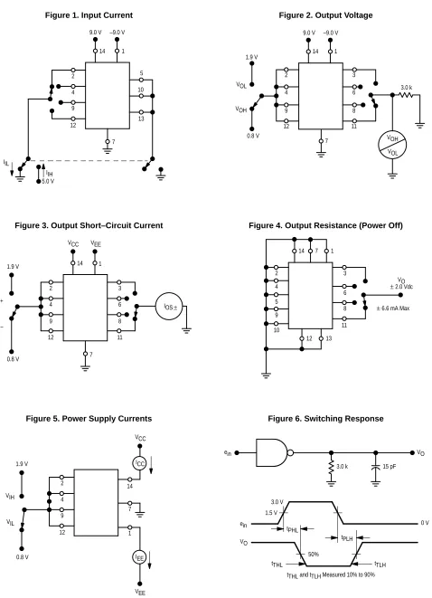
CHARACTERISTIC DEFINITIONS
Figure 1. Input Current Figure 2. Output Voltage
Figure 3. Output Short–Circuit Current Figure 4. Output Resistance (Power Off)
Figure 5. Power Supply Currents Figure 6. Switching Response
10
13 9
4
12
5 1
2
14 9.0 V
5.0 V IIH IIL
–9.0 V
7
1.9 V
7 VOL
9.0 V
VOH 0.8 V
VOL 3.0 k
VOH
14 1
–9.0 V
2
4
9
12
3
6
8
11
9 2
14
4
5 IOS +
1
11 6
8
13 9
4
12
3 1
± 6.6 mA Max 3
7 8 6
11
0.8 V
2
1.9 V 14
VEE VCC
7
10
12 IOS±
VO
± 2.0 Vdc
IOS –
tTHL and tTLH Measured 10% to 90% VO
15 pF 3.0 k
50% tPHL
tPLH
tTLH tTHL
ein
0 V 3.0 V
1.5 V
ein
VO ICC
VIL
2
VCC
1 14
7
12 4
9
IEE
VEE 1.9 V
VIH
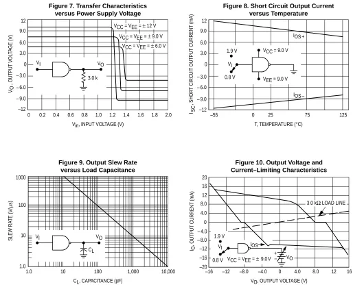
TYPICAL CHARACTERISTICS (TA = +25°C, unless otherwise noted.)
2.0 1.8 1.6 1.4 1.2 0.4
0.2 0.6 0.8 1.0 – 9.0 – 3.0 0 3.0 6.0 –12 9.0 12 – 6.0 0
VCC = VEE = ± 12 V
Vin, INPUT VOLTAGE (V)
V , OUTPUT
VOL
TAGE (V)
O
[image:4.612.48.562.80.499.2]VCC = VEE = ± 9.0 V VCC = VEE = ± 6.0 V
Figure 7. Transfer Characteristics versus Power Supply Voltage
VI VO 3.0 k IOS – 12 9.0 6.0 3.0 0 – 3.0 – 6.0 – 9.0 –12 125 IOS + 75
–55 0 25
T, TEMPERATURE (°C)
I , SHOR
T CIRCUIT OUTPUT CURRENT (mA) SC
Figure 8. Short Circuit Output Current versus Temperature
VEE = 9.0 V 0.8 V
VI
1.9 V VCC = 9.0 V
1000
1.0 100 1,000 10,000
CL, CAPACITANCE (pF) 10 10 100 1.0 SLEW RA TE (V/ s) µ
Figure 9. Output Slew Rate versus Load Capacitance
VI VO CL 12 0 – 4.0 – 8.0 –12 –16 –20 4.0 8.0 16
–16 –12 –8.0 –4.0 4.0 12
16
8.0 20
0
3.0 kΩ LOAD LINE
VO, OUTPUT VOLTAGE (V)
I , OUTPUT
CURRENT (mA) O VO IOS 1.9 V
VCC = VEE = ± 9.0 V 0.8 V
VI
+ –
Figure 10. Output Voltage and Current–Limiting Characteristics 25 4.0 6.0 8.0 10 12 14
–55 75 125
2.0
0 16
T, TEMPERATURE (°C)
V , V , POWER SUPPL
[image:4.612.197.429.536.720.2]Y VOL TAGE (V) CC EE 0 VEE 1 3.0 k 3.0 k 3.0 k 3.0 k 14 VCC 8 6 3 11 7
APPLICATIONS INFORMATION
The Electronic Industries Association EIA–232D specification details the requirements for the interface between data processing equipment and data communications equipment. This standard specifies not only the number and type of interface leads, but also the voltage levels to be used. The MC1488 quad driver and its companion circuit, the MC1489 quad receiver, provide a complete interface system between DTL or TTL logic levels and the EIA–232D defined levels. The EIA–232D requirements as applied to drivers are discussed herein.
The required driver voltages are defined as between 5.0 and 15 V in magnitude and are positive for a Logic “0” and negative for a Logic “1.” These voltages are so defined when the drivers are terminated with a 3000 to 7000 Ω resistor. The MC1488 meets this voltage requirement by converting a DTL/TTL logic level into EIA–232D levels with one stage of inversion.
The EIA–232D specification further requires that during transitions, the driver output slew rate must not exceed 30 V per microsecond. The inherent slew rate of the MC1488 is much too fast for this requirement. The current limited output of the device can be used to control this slew rate by connecting a capacitor to each driver output. The required capacitor can be easily determined by using the relationship C = IOS x ∆T/∆V from which Figure 12 is derived. Accordingly, a 330 pF capacitor on each output will guarantee a worst case slew rate of 30 V per microsecond.
1000
10 100
1.0 10
[image:5.612.325.561.153.362.2]333 pF 30 V/µs
Figure 12. Slew Rate versus Capacitance for ISC = 10 mA
C, CAPACITANCE (pF)
10,000
100 1,000
1.0
SLEW RA
TE (V/
s)
µ
The interface driver is also required to withstand an accidental short to any other conductor in an interconnecting cable. The worst possible signal on any conductor would be another driver using a plus or minus 15 V, 500 mA source. The MC1488 is designed to indefinitely withstand such a short to all four outputs in a package as long as the power supply voltages are greater than 9.0 V (i.e., VCC q 9.0 V; VEE p – 9.0 V). In some power supply designs, a loss of system power causes a low impedance on the power supply outputs. When this occurs, a low impedance to ground would exist at the power inputs to the MC1488 effectively shorting the 300 Ω output resistors to ground. If all four outputs were then shorted to plus or minus 15 V, the power dissipation in these resistors would be excessive. Therefore, if the system is designed to permit low impedances to ground at the power supplies of the drivers, a diode
should be placed in each power supply lead to prevent overheating in this fault condition. These two diodes, as shown in Figure 13, could be used to decouple all the driver packages in a system. (These same diodes will allow the MC1488 to withstand momentary shorts to the
± 25 V limits specified in the earlier Standard EIA–232B.) The addition of the diodes also permits the MC1488 to withstand faults with power supplies of less than the 9.0 V stated above.
Figure 13. Power Supply Protection to Meet Power Off Fault Conditions
VCC 14
MC1488
VEE 7
MC1488 14
MC1488 14
7
1 1 7 1
The maximum short circuit current allowable under fault conditions is more than guaranteed by the previously mentioned 10 mA output current limiting.
Other Applications
The MC1488 is an extremely versatile line driver with a myriad of possible applications. Several features of the drivers enhance this versatility:
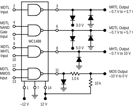
1. Output Current Limiting – this enables the circuit designer to define the output voltage levels independent of power supplies and can be accomplished by diode clamping of the output pins. Figure 14 shows the MC1488 used as a DTL to MOS translator where the high level voltage output is clamped one diode above ground. The resistor divider shown is used to reduce the output voltage below the 300 mV above ground MOS input level limit.
[image:5.612.58.298.323.505.2]Figure 14. MDTL/MTTL–to–MOS Translator Figure 15. Logic Translator Applications
MOS Output (with VSS = GND)
10 k 1.0 k
MDTL MTTL Input
1/4 MC1488 12 V
– 12 V – 12 V
MOS Output –10 V to 0 V MDTL Output – 0.7 V to + 5.7 V
MHTL Output – 0.7 V to 10 V MRTL Output – 0.7 V to + 3.7 V
–12 V
10 k 1.0 k
5.0 V 8
1
11
6 3.0 V
3
MC1488
13 12 10 9 5 4
MDTL MMOS Input
MDTL MHTL Input
2
MDTL NAND Gate Input MDTL Input
OUTLINE DIMENSIONS
NOTES:
1. LEADS WITHIN 0.13 (0.005) RADIUS OF TRUE POSITION AT SEATING PLANE AT MAXIMUM MATERIAL CONDITION.
2. DIMENSION L TO CENTER OF LEADS WHEN FORMED PARALLEL.
3. DIMENSION B DOES NOT INCLUDE MOLD FLASH.
4. ROUNDED CORNERS OPTIONAL.
1 7
14 8
B
A
F
H G D
K C
N
L
J
M SEATING
PLANE
DIM MIN MAX MIN MAX MILLIMETERS INCHES
A 0.715 0.770 18.16 19.56 B 0.240 0.260 6.10 6.60 C 0.145 0.185 3.69 4.69 D 0.015 0.021 0.38 0.53 F 0.040 0.070 1.02 1.78 G 0.100 BSC 2.54 BSC H 0.052 0.095 1.32 2.41 J 0.008 0.015 0.20 0.38 K 0.115 0.135 2.92 3.43 L 0.300 BSC 7.62 BSC M 0 10 0 10 N 0.015_ 0.039_ 0.39_ 1.01_
NOTES:
1. DIMENSIONING AND TOLERANCING PER ANSI Y14.5M, 1982.
2. CONTROLLING DIMENSION: MILLIMETER. 3. DIMENSIONS A AND B DO NOT INCLUDE
MOLD PROTRUSION.
4. MAXIMUM MOLD PROTRUSION 0.15 (0.006) PER SIDE.
5. DIMENSION D DOES NOT INCLUDE DAMBAR PROTRUSION. ALLOWABLE DAMBAR PROTRUSION SHALL BE 0.127 (0.005) TOTAL IN EXCESS OF THE D DIMENSION AT MAXIMUM MATERIAL CONDITION. –A–
–B–
G
P7 PL
14 8
7
1 0.25 (0.010)M B M
S B M
0.25 (0.010) T A S –T–
F RX 45
SEATING
PLANE D14 PL K
C
J M
_ DIM MIN MAX MIN MAX
INCHES MILLIMETERS
A 8.55 8.75 0.337 0.344 B 3.80 4.00 0.150 0.157 C 1.35 1.75 0.054 0.068 D 0.35 0.49 0.014 0.019 F 0.40 1.25 0.016 0.049 G 1.27 BSC 0.050 BSC J 0.19 0.25 0.008 0.009 K 0.10 0.25 0.004 0.009 M 0 7 0 7 P 5.80 6.20 0.228 0.244 R 0.25 0.50 0.010 0.019
_ _ _ _
P SUFFIX PLASTIC PACKAGE
CASE 646–06 ISSUE L
D SUFFIX PLASTIC PACKAGE
Motorola reserves the right to make changes without further notice to any products herein. Motorola makes no warranty, representation or guarantee regarding the suitability of its products for any particular purpose, nor does Motorola assume any liability arising out of the application or use of any product or circuit, and specifically disclaims any and all liability, including without limitation consequential or incidental damages. “Typical” parameters can and do vary in different applications. All operating parameters, including “Typicals” must be validated for each customer application by customer’s technical experts. Motorola does not convey any license under its patent rights nor the rights of others. Motorola products are not designed, intended, or authorized for use as components in systems intended for surgical implant into the body, or other applications intended to support or sustain life, or for any other application in which the failure of the Motorola product could create a situation where personal injury or death may occur. Should Buyer purchase or use Motorola products for any such unintended or unauthorized application, Buyer shall indemnify and hold Motorola and its officers, employees, subsidiaries, affiliates, and distributors harmless against all claims, costs, damages, and expenses, and reasonable attorney fees arising out of, directly or indirectly, any claim of personal injury or death associated with such unintended or unauthorized use, even if such claim alleges that Motorola was negligent regarding the design or manufacture of the part. Motorola and are registered trademarks of Motorola, Inc. Motorola, Inc. is an Equal Opportunity/Affirmative Action Employer.
How to reach us:
USA / EUROPE: Motorola Literature Distribution; JAPAN: Nippon Motorola Ltd.; Tatsumi–SPD–JLDC, Toshikatsu Otsuki,
P.O. Box 20912; Phoenix, Arizona 85036. 1–800–441–2447 6F Seibu–Butsuryu–Center, 3–14–2 Tatsumi Koto–Ku, Tokyo 135, Japan. 03–3521–8315