1891 ISSN: 2278 – 7798 All Rights Reserved © 2015 IJSETR
Implementation of SVPWM Based Three Phase
Inverter Using 8 Bit Microcontroller
Prof. S. K. Patil1, Mr. Nikhil D. Wadokar2, Miss. Pallavi H. Pikale3
Associate Professor1, P.G. Scholor2, P.G. Scholor3
Department of Electrical Engineering, Government College of Engineering, Karad, Maharashtra, India123
Abstract: This paper describes the digital implementation of Space Vector Pulse Width Modulation (SVPWM) technique using 8-bit microcontroller for three-phase inverter. For control of IM number of Pulse width modulation (PWM) schemes are used to variable voltage and frequency supply. The most commonly used PWM schemes for three-phase voltage source inverters (VSI) are sinusoidal PWM (SPWM) and space vector PWM (SVPWM). There is an increasing trend of using space vector PWM (SVPWM) because of it reduces harmonic content in voltage, increases fundamental output voltage by 15% & smooth control of IM. So, here present the implementation of SVPWM based three phase inverter using simple microcontroller 89c51. This paper presents simulation and hardware results of this technique.
Keywords—Space Vector Pulse Width Modulation (SVPWM), Proteus, Inverter, VSI.
I. INTRODUCTION
DC to AC converter is known as inverters. The Function of an inverter is to change dc input voltage to a symmetric ac output voltage of desired magnitude and frequency. The output voltage could be fixed or variable at fixed or variable frequency. A variable output voltage can be obtained by varying the dc input voltage and maintaining the gain of inverter constant. On other hand, if the dc input voltage is fixed and it is not controllable, a variable output voltage can be obtained by varying the gain of inverter, which is normally accomplished by pulsed width modulation (PWM) control within the inverter [4]. Based on operation; Inverters are of two types Voltage Source Inverters (VSI) & Current Source Inverters (CSI). An inverter is called VSI if the input voltage remain constant, a CSI if the input current is maintained constant. Out of which VSI is widely used in industries as it gives independently controlled AC output is a voltage [5]. The performance parameters of an inverter such as switching losses and harmonic reduction are principally depended on the modulation strategies used to control the inverter. In this design the Space vector pulse width modulation (SVPWM) technique has been used for controlling the inverter as it can be directly controlled the inverter output voltage and output frequency according to the space vector .VSI usually operate on Pulse Width Modulation (PWM) technique. In this is method a fixed dc input voltage is given to an inverter and the output is a controlled ac voltage. There are different PWM techniques for control the inverter and its output harmonic reduction. The most widely used switching techniques are the Sinusoidal PWM (SPWM) and the Space Vector PWM (SVPWM). There are number of industry
applications in which induction motors are fed by Space Vector Pulse Width Modulated inverter. It provides many benefits to their users such as simplicity of circuit, reduced energy consumption etc. In this paper firstly Space Vector Pulse Width Modulation (SVPWM) techniques for three phase inverter is described. Later the hardware requirement has discussed. In last part hardware result have been explained.
II. SVPWM TECHNIQUE
Space vector modulation is quite different from PWM methods. With PWMs, inverter can be thought as three separate push-pull driver stages, which create each phase waveform independently. SVM, however, treats the inverter as a single unit; specifically inverter can be driven to eight unique states. Modulation is accomplishes by switching the state of the inverter. The control strategies are implemented in digital systems. SVM is a digital modulating technique where the objective is to generate PWM load line voltages that are in average equal to given load line voltages. This is done in each sampling period by properly selecting the switching states of the inverter and calculation of the appropriate time period for each state. The selection of the states and their time period are accomplished by the space vector (SV) transformation.
Space Transformation
Any three functions of time that satisfy
t u
t u
t 0u
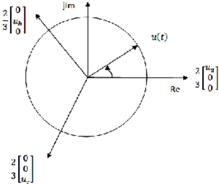
a b cCan be represented in two dimensional space. The coordinates are similar to those of three phase voltages such that the vector [ua 0 0]t is placed along the x-axis, the vector [0ub 0]t is phase shifted by 1200, and the vector the [00 uc]t is phase shifted by 2400 .This is shown in figure 1. SV in complex notation is given by
1892 ISSN: 2278 – 7798 All Rights Reserved © 2015 IJSETR
𝑢 𝑡 = 2
3 𝑢𝑎+ 𝑢𝑏𝑒
𝑗 2 3 𝜋 + 𝑢
𝑐𝑒−𝑗 2 3 𝜋 (1) Where 2/3 is scaling factor.
Eq. (1) can be written in real and imaginary components in x-y domain as
𝑢 𝑡 = 𝑢𝑥+ 𝑗𝑢𝑦 (2) Using Eqs. (1) and (2), we can obtain the coordinate
transformation from a-b-c –axis to x-y axis as given by 𝑢𝑥 𝑢𝑦 = 2 3 1 −1 2 −1 2 0 3 2 − 3 2 𝑢𝑎 𝑢𝑏 𝑢𝑐 (3)
This can be written as 𝑢𝑥= 2 3 𝑣𝑎− 0.5 𝑣𝑏+ 𝑣𝑐 (4) 𝑢𝑦= 3 2 𝑣𝑏− 𝑣𝑐 (5) The transformation from the x-y axis to the α-β axis, which
is rotating with an angular velocity of ω, can be obtained by 𝑢𝛼 𝑢𝛽 = 𝑐𝑜𝑠 𝜔𝑡 𝑐𝑜𝑠 𝜋 2− 𝜔𝑡 𝑠𝑖𝑛 𝜔𝑡 𝑠𝑖𝑛 𝜋 2+ 𝜔𝑡 (6)
Using Eq. (1), we can find the inverse transformation as
𝑢𝑎 = 𝑅𝑒 𝑢 (7) 𝑢𝑏 = 𝑅𝑒 𝑢𝑒−𝑗 2 3 𝜋 (8)
𝑢𝑐 = 𝑅𝑒 𝑢𝑒𝑗 2 3 𝜋 (9) Then, using Eq. (1), we get the space vector representation
as
𝑢 𝑡 = 𝑉𝑚𝑒𝑗𝜃 = 𝑉𝑚𝑒𝑗𝜔𝑡 (10) which is a vector of magnitude 𝑉𝑚 rotating at a constant speed 𝜔 in rads per second.
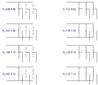
Figure 2: The on and off states of the inverter switches. A. Space vector (SV)
The switching states of the inverter can be represented by binary values q1, q2, q3, q4, q5, and q6; that is, qk = 1 when a switch is turned on and qk = 0 when a switched is turned off. The pair of q1q4, q3q6 and q5q2 are complimentary. Therefore,
q4 = 1 - q1, q6 = 1 - q3 and q2 = 1 – q5. The switch on and off states are shown in figure 2.
Using three phase to two phase transformation in Eq. (3) and the line voltage as the reference, the α-β components of the RMS output voltage vector can be expressed as a function of q1, q3, and q5.
𝑉𝐿𝛼 𝑉𝐿𝛽 = 2 3 3 2 𝑉 1 −1 2 −1 2 0 3 2 − 3 2 3×2 𝑞1 𝑞2 𝑞3 (11)
Using the factor 2 for converting the rms voltage to its peak value, the peak value of the line voltage is 𝑉𝐿 𝑝𝑒𝑎𝑘 = 2𝑉𝑠 and that of the phase voltage is 𝑉3 𝑝 𝑝𝑒𝑎𝑘 = 𝑉𝑠 3. Using the phase voltage 𝑉𝑎 as the reference, which usually the case, the line voltage vector 𝑉𝑎𝑏 leads the phase vector by 𝜋 6 . The normalized peak value of the nth line voltage vector can be found from
𝑉𝑛 = 2× 2 3 𝑒 𝑗 2𝑛−1 𝜋 6 = 2 3 𝑐𝑜𝑠 2𝑛−1 𝜋 6 + 𝑗𝑠𝑖𝑛 2𝑛−1 𝜋 6 (12) For n = 0,1,2,6
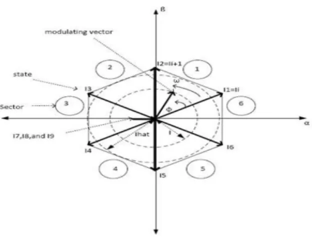
There are six nonzero vectors, 𝑉1− 𝑉6, and two zero vectors, 𝑉0 and 𝑉7, as shown in figure 3. Let us define a performance vector U as the time integral function of 𝑉𝑛 such that
1893 ISSN: 2278 – 7798 All Rights Reserved © 2015 IJSETR
Figure 3: The space vector representation
Where 𝑈0 is the initial condition. According to Eq.(13). U draws a hexagon locus that is determined by the magnitude and the time period of the voltage vectors. If the output voltages are purely sinusoidal, then the performance vector U becomes
𝑈∗= 𝑀𝑒𝑗𝜃 = 𝑀𝑒𝑗𝜔𝑡
(14) Where 𝑀 is the modulation index 0 < 𝑀 < 1 for
controlling the amplitude of the output voltage and 𝜔 is the output frequency in rads per second. 𝑈∗
draws a pure circle locus as shown in figure 3 by dotted circle of radius 𝑀 = 1 and it becomes the reference vector 𝑉𝑟. The locus 𝑈 can be controlled by selecting 𝑉𝑛 and adjusting the time width of 𝑉𝑛 to follow the 𝑈∗ locus as closely as possible. This is called quasi-circular locus method.
B. Modulating reference vectors
Using Eqs. (3), (4) and (5), the vectors of three-phase
line modulating signals 𝑉𝑟 𝑎𝑏𝑐 = 𝑉𝑟𝑎 𝑉𝑟𝑏 𝑉𝑟𝑐 𝑇 can be represented by the complex vector 𝑈∗= 𝑉
𝑟= 𝑣𝑟 𝛼𝛽 = 𝑣𝑟𝛼 𝑣𝑟𝛽 𝑇 as given by 𝑣𝑟𝛼 = 2 3 𝑣𝑟𝑎− 0.5 𝑣𝑟𝑏+ 𝑣𝑐𝑟 (15) 𝑣𝑟𝛽 = 3 2 𝑣𝑟𝑏− 𝑣𝑟𝑐 (16) If the line modulating signals 𝑣𝑟 𝑎𝑏𝑐 are three balanced
sinusoidal waveforms with an amplitude of 𝐴𝑐= 1 and an angular frequency 𝜔, the resulting modulating signal in the 𝛼 − 𝛽 stationary frame 𝑉𝑐= 𝑣𝑟 𝛼𝛽 becomes a vector of fixed amplitude 𝑀𝐴𝑐= = 𝑀 that rotates at frequency 𝜔.
C. SV switching
The objective of the SV switching is to approximate the sinusoidal line modulating signal Vr with eight space vectors 𝑉𝑛, 𝑛 = 0,1,2, … . ,7 . However, if the modulating signal 𝑉𝑐 is laying between the arbitrary vectors 𝑉𝑛 and 𝑉𝑛 +1, then the two nonzero vectors 𝑉𝑛 𝑎𝑛𝑑 𝑉𝑛 +1 and one
zero SV (𝑉𝑧 = 𝑉0 𝑜𝑟 𝑉7) should be used to obtain the maximum load line voltage and to minimize the switching frequency. As an example, a voltage vector 𝑉𝑟 in section one can be realized by the 𝑉1 and 𝑉2 vectors and one of the two null vectors 𝑉0 𝑜𝑟 𝑉7 . In other words, 𝑉1 is active for time 𝑇1, 𝑉2 is active for 𝑇2, and one of the null vectors 𝑉0 𝑜𝑟 𝑉7 is active for 𝑇𝑧. For sufficiently high-switching frequency, the reference vector 𝑉𝑟 can be assumed constant during one switching period. Because the vectors 𝑉1 and 𝑉2 are constant and 𝑉𝑧 = 0, we can equate the volt time of the reference vector to the SVs as
𝑉𝑟× 𝑇𝑠= 𝑉1× 𝑇1+ 𝑉2× 𝑇2+ 𝑉𝑧× 𝑇𝑧
which is defined as the SVM. This is achieved by using two adjacent SVs with appropriate duty cycle. The vector diagram is shown in Figure 3. Expressing the SVs in rectangular coordinates, above eq. becomes
𝑇𝑠𝑀 𝑐𝑜𝑠 𝜋 6+ 𝜃 𝑠𝑖𝑛 𝜋 6+ 𝜃 = 𝑇1 2 3 𝑐𝑜𝑠 𝜋 6 𝑠𝑖𝑛 𝜋6 + 2 3 𝑐𝑜𝑠 𝜋 2 𝑠𝑖𝑛 𝜋 2 (17)
Figure 4: Determination of state times
Equating the real and imaginary parts on both sides, we get 𝑇𝑠𝑀𝑐𝑜𝑠 𝜋 6+ 𝜃 = 𝑇1 2 3𝑐𝑜𝑠 𝜋 6 + 𝑇2 2 3𝑐𝑜𝑠 𝜋 2 𝑇𝑠𝑀𝑠𝑖𝑛 𝜋 6+ 𝜃 = 𝑇1 2 3𝑠𝑖𝑛 𝜋 6 + 𝑇2 2 3𝑠𝑖𝑛 𝜋 2 Solving for 𝑇1 and 𝑇2, we get
𝑇1= 𝑇𝑠𝑀 3 2 𝑐𝑜𝑠 𝜋 6+𝜃 𝑐𝑜𝑠 𝜋6 = 𝑇𝑠𝑀𝑐𝑜𝑠 𝜋 6+ 𝜃 = 𝑇𝑠𝑀 sin 𝜋 3− 𝜃 (18) 𝑇2= 𝑇𝑠𝑀 3 2 sin 𝜃 sin 𝜋 6 = 𝑇𝑠𝑀 sin 𝜃 (19) 𝑇0= 𝑇𝑧 = 𝑇𝑠− 𝑇1− 𝑇2 (20) Where 𝑀 is the modulation index;
𝜃 is the angle between 𝑉𝑟 and 𝑉𝑛; 𝑇𝑠 is the switching or sampling period
1894 ISSN: 2278 – 7798 All Rights Reserved © 2015 IJSETR
The same rule can be applied for calculating the time states of the vectors in sectors 2 or 6. It is assumed that the inverter operates at constant frequency and 𝑇𝑠 remains constant.
D. SV sequence.
The SV sequence should assure that the load line voltages have the quarter-wave symmetry to reduce even harmonics in their spectra. To reduce the switching frequency, it is also necessary to arrange the switching sequence in such a way that the transition from one to the next is performed by switching only one inverter leg at a time. Although there is not symmetric approach to generate an SV sequence, these conditions are met by the sequence 𝑉𝑧 ,𝑉𝑛, 𝑉𝑛 +1, 𝑉𝑧. If for example, the reference vector falls in section 1, the switching sequence is V0, V1, V2, V7, V7, V2, V1, V0.The time period 𝑇𝑧 can be split and distributed at the beginning and at the end of sampling period 𝑇𝑠. Figure 5 shows both the sequence and the segments of three phase output voltages during two sampling periods. In general, the time intervals of the null vectors are equally distributed, as shown in Figure 5, with 𝑇𝑧 at the beginning and 𝑇2 𝑧 at the end. 2
Figure 5: Pattern of SVM
III. HARDWARE IMPLEMENTATION
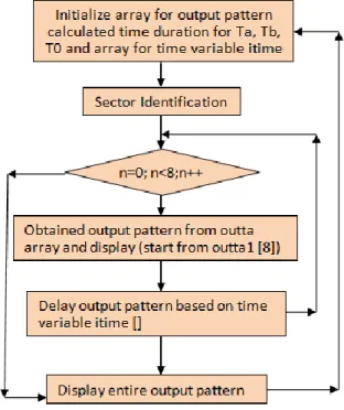
SVPWM technique is implemented using simple microcontroller 89c51. Output pattern of SVPWM is store in the form of lookup table. Time durations are calculated as explained before and stored in lookup table. These times duration used to provide on time of switches. Timer 0 of 89c51 is used to provide delay according to calculated time durations. Flow chart shows actual implementation of SVPWM.
Figure 6: Flow Chart
IV. SIMULATION RESULTS
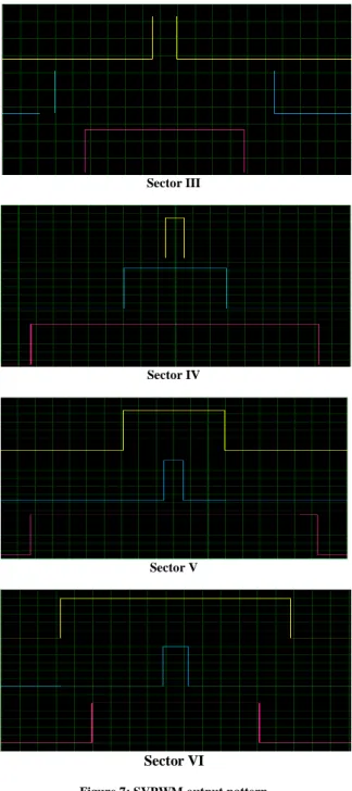
Results are obtained using proteus. Actual switching pattern for all six sectors are shown below.
Sector I
1895 ISSN: 2278 – 7798 All Rights Reserved © 2015 IJSETR
Sector III
Sector IV
Sector V
Sector VI
Figure 7: SVPWM output pattern
Actual hardware is as shown below
Figure 8: SVPWM Hardware Photo
V. CONCLUSION
This paper describes the digital implementation of SVPWM technique for three-phase inverter. The proposed system uses 8-bit 89c51 microcontroller for generating SVPWM signal needed to trigger the gates of MOSFET bridge of the inverter. The experimental results show the ability of the proposed system to generate a three-phase sine wave signal with desired frequency.
REFERENCES
1] Sandeep N Panchal, Vishal S Sheth, Akshay A Pandya, “Simulation Analysis of SVPWM Inverter Fed Induction Motor Drives” International Journal of Emerging Trends in Electrical and Electronics (IJETEE), Vol. 2, Issue. 4, April-2013.
2] Mahmoud Gaballah, Mohammed El-Bardini, Soliman Sharaf and Mohammed Mabrouk, “implementation of space vector pwm for Driving two level voltage source inverters”, Journal of Engineering Sciences, Assiut University, Vol. 39, No. 4, pp.871-884, July 2011. 3] Mahesh A. Patel, Ankit R. Patel, Dhaval R. Vyas and Ketul M.
Patel,” Use of PWM Techniques for Power Quality Improvement” International Journal of Recent Trends in Engineering, Vol. 1, No. 4, May 2009.
4] M. H. Rashid, "Power Electronic, Circuits, Devices, and Applications", Second Edition, Printice-Hall of India, New Delhi, 1994.
5] Marwan A.A. Badran, Ahmad M. Tahir and Waleed F. Faris,” Digital Implementation of Space Vector Pulse Width Modulation Technique Using 8-bit Microcontroller”, World Appl. Sci. J., 21 (Mathematical Applications in Engineering): 21-28, 2013.
6] K. Mounika, B. Kiran Babu, “Sinusoidal and Space Vector Pulse Width Modulation for Inverter”,International Journal of Engineering Trends and Technology (IJETT) – Volume 4 Issue 4 - April 2013. 7] Mohan, N., “First Course on Power Electronics and Drives,”
MNPERE, 2003.
8] Bimal K. Bose,"Power Electronics and Motor Drives, Advances and Trends,by: Based Expert System Using Object Oriented ProgrammingLanguage”,2006.