Advances in Radio Science (2003) 1: 171–175 c
Copernicus GmbH 2003
Advances in
Radio Science
Performance analysis of general purpose and digital signal
processor kernels for heterogeneous systems-on-chip
T. von Sydow, H. Blume, and T. G. Noll
Electrical Engineering and Computer Systems, RWTH Aachen University, Schinkelstr. 2, 52062 Aachen, Germany
Abstract. Various reasons like technology progress, flexi-bility demands, shortened product cycle time and shortened time to market have brought up the possibility and necessity to integrate different architecture blocks on one heteroge-neous System-on-Chip (SoC). Architecture blocks like pro-grammable processor cores (DSP- and GPP-kernels), embed-ded FPGAs as well as embed-dedicated macros will be integral parts of such a SoC. Especially programmable architecture blocks and associated optimization techniques are discussed in this contribution. Design space exploration and thus the choice which architecture blocks should be integrated in a SoC is a challenging task. Crucial to this exploration is the evalu-ation of the applicevalu-ation domain characteristics and the costs caused by individual architecture blocks integrated on a SoC. An ATE-cost function has been applied to examine the per-formance of the aforementioned programmable architecture blocks. Therefore, representative discrete devices have been analyzed. Furthermore, several architecture dependent op-timization steps and their effects on the cost ratios are pre-sented.
1 Introduction
In today’s high-performance and computational intensive systems for e.g. video processing or wireless communica-tion a high degree of flexibility and highest computacommunica-tional capabilities have to be provided. But the computational de-mands are and will be well beyond the performance of pro-grammable processor kernels (Davis et al., 2001; Keutzer et al., 2000). Future generations of e.g. communication stan-dards strengthen this computational gap. On the other hand in addition to these computational demands a high degree of flexibility is required. With a sufficient degree of flexibility it is possible to add new features and to adapt the chang-ing demands of future systems without designchang-ing a new plat-Correspondence to: T. von Sydow
form and thus increasing the product life time. Therefore, reconfigurable logic and programmable devices which are able to meet these requirements are important components in modern heterogeneous SoCs. Generally, dedicated hard-ware implementations offer orders of magnitude better com-putational performance at orders of magnitude lower power dissipation. But flexibility of those implementations is re-stricted to weak programmability.
Altogether, a well-balanced architecture of a sophisticated, high performance SoC has to include different types of these architecture blocks in order to provide the required perfor-mance (throughput rate) at reasonable costs (area, power dis-sipation) on one hand and ensuring sufficient flexibility on the other.
Partitioning a system in system blocks and mapping these system blocks on adequate architecture blocks is a challeng-ing task discussed e.g. in the correspondchalleng-ing paper within this proceedings (Feldk¨amper et al., 2002). In this contribution an ATE-cost function which is the product of chip area, clock period and energy per calculated sample has been applied to determine quantitative results for architecture blocks whose features in terms of several parameters are depicted qualita-tively in Fig. 1. In this paper we will focus on the metrics of programmable kernels. In the following especially features of programmable architecture blocks (see Sect. 2) will be ex-amined. Therefore, an exemplary device from each category (GPP, DSP, ASIP) is considered.
2 Optimization
172 T. von Sydow et al.: Performance analysis
Performance Analysis of General Purpose and Digital Signal
Processor Kernels for heterogeneous Systems-on-Chip
T. von Sydow, H. Blume, T. G. Noll
Chair of Electrical Engineering and Computer Systems, RWTH Aachen University Schinkelstr. 2, 52062 Aachen, Germany
Email: {sydow, blume, tgn}@eecs.rwth-aachen.de
Abstract. Various reasons like technology progress, flexibility demands, shortened product cycle time and shortened time to market have brought up the possibility and necessity to integrate different architecture blocks on one heterogeneous System-on-Chip (SoC). Architecture blocks like programmable processor cores (DSP- and GPP-kernels), embedded FPGAs as well as dedicated macros will be integral parts of such a SoC. Especially programmable architecture blocks and associated optimization techniques are discussed in this contribution. Design space exploration and thus the choice which architecture blocks should be integrated in a SoC is a challenging task. Crucial to this exploration is the evaluation of the application domain characteristics and the costs caused by individual architecture blocks integrated on a SoC. An ATE-cost function has been applied to examine the performance of the aforementioned programmable architecture blocks. Therefore, representative discrete devices have been analyzed. Furthermore, several architecture dependent optimization steps and their effects on the cost ratios are presented.
1 Introduction
In today's high-performance and computational intensive systems for e.g. video processing or wireless communication a high degree of flexibility and highest computational capabilities have to be provided. But the computational demands are and will be well beyond the performance of programmable processor kernels (Davis, R, et al., 2001; Keutzer, K., et al., 2000). Future generations of e.g. communication standards strengthen this computational gap. On the other hand in addition to these computational demands a high degree of flexibility is required. With a sufficient degree of flexibility it is possible to add new features and to adapt the changing demands of future systems without designing a new platform and thus increasing the product life time. Therefore, reconfigurable logic and programmable devices which are able to meet these requirements are important components in modern heterogeneous SoCs. Generally, dedicated hardware implementations offer or-ders of magnitude better computational performance at oror-ders of magnitude lower power dissipation. But flexibility of those implementations is restricted to weak programmability.
Altogether, a well-balanced architecture of a sophisticated, high performance SoC has to include different types of these architecture blocks in order to provide the required performance (throughput rate) at reasonable costs (area, power dissipation) on one hand and ensuring sufficient flexibility on the other.
Log P E R F O R M A N C E
L
og
F L
E X I B I L
I T
Y
Lo
g P O
W E R D
I S S I P A
T I O
N Application Specific Signal Processor Core Digital Signal Processor Core General Purpose Processor Core Embedded FPGA Standard Cell Macro Physically Optimized Macro
102 MOPS 106 MOPS
10-3 h-1
1 h-1
10-3 W 102 W
Figure 1. Trade-off between flexibility, performance and power consumption
Partitioning a system in system blocks and mapping these system blocks on adequate architecture blocks is a challenging task discussed e.g. in the corresponding paper within this proceedings (Feldkämper, H., et al.; 2002). In this contribution an ATE-cost function which is the product of chip area, clock period and energy per calculated sample has been applied to determine quantitative results for architecture blocks whose features in
programmable architecture blocks
Fig. 1. Trade-off between flexibility, performance and power con-sumption.
unoptimized
Utilization of issue slots Utilization of issue slots
cl o ck cy cl e s 1 5 10 optimized a) b)
Fig. 2. Critical path diagram of the non-optimized (a) and optimized (b) add/reg operation.
2.1 ASIP
The Trimedia (Trimedia website) is a so-called Application Specific Instruction Set Processor (ASIP) developed for ap-plications out of the multimedia domain. Therefore, video and audio interfaces already have been integrated. Addition-ally, the Trimedia ASIP contains a coprocessor most suitable for video and audio signal processing tasks. The processor core is based on a VLIW architecture including five issue slots. Hence, up to five different instructions could be exe-cuted per cycle.
Figure 2 shows the so-called critical path diagram of a loop. This loop of an exemplary add/reg-operation, which consists of basic arithmetical and register transfer operations applied in (Feldk¨amper et al., 2000) amounts for 88% of the total execution time. The utilization of the available is-sue slots with ASIP specific operations is depicted. Opera-tions are visualized by boxes and the interdependencies be-tween them are depicted by lines. The critical path diagram depicted in Fig. 2b could be achieved by performing ASIP suited software optimization steps such as software pipelin-ing, common subexpression elimination and application of custom operations. Also power dissipation was examined for different code versions (Fig. 3). With each
optimiza-terms of several parameters are depicted qualitatively in Figure 1. In this paper we will focus on the metrics of
programmable kernels. In the following especially features of programmable architecture blocks (see section 2)
will be examined. Therefore, an exemplary device from each category (GPP, DSP, ASIP) is considered.
2 Optimization
Several optimization steps have been applied individually to ensure that the considered programmable
architecture blocks nearly perform optimally in terms of throughput rate and power dissipation. In the following,
three exemplary devices and associated optimization techniques are presented.
2.1 ASIP
The Trimedia (Trimedia website) is a so-called Application Specific Instruction Set Processor (ASIP) developed
for applications out of the multimedia domain. Therefore, video and audio interfaces already have been
integrated. Additionally, the Trimedia ASIP contains a coprocessor most suitable for video and audio signal
processing tasks. The processor core is based on a VLIW architecture including five issue slots. Hence, up to
five different instructions could be executed per cycle.
Figure 2 shows the so-called critical path diagram of a loop. This loop of an exemplary add/reg-operation, which
consists of basic arithmetical and register transfer operations applied in (Feldkämper, H.T., et al., 2000) amounts
for 88 % of the total execution time. The utilization of the available issue slots with ASIP specific operations is
depicted. Operations are visualized by boxes and the interdependencies between them are depicted by lines. The
critical path diagram depicted in Figure 2b could be achieved by performing ASIP suited software optimization
steps such as software pipelining, common subexpression elimination and application of custom operations.
Also power dissipation was examined for different code versions (Figure 3). With each optimization step the
execution time decreases which was mainly accomplished by an improvement of the instruction level
parallelism. This leads to an increase of the power dissipation. However, the consumed energy per sample
decreases with each optimization step. This is due to the fact, that the number of achieved output samples per
time increases more decisively than the power dissipation. The energy per sample is the metric which has to be
chosen instead of the power consumption.
unoptimized
Utilization of issue slots Utilization of issue slots
cl o ck cy cl e s 1 5 10 optimized a) b) 3,4 3,5 3,6 3,7 3,8 3,9 4 4,1
2 4 6 8
sample rate [MHz]
po w e r di ss ip at io n [ W ] 0 0,2 0,4 0,6 0,8 1 1,2 1,4 en er gy/ sa m pl e [ uJ /s am pl e]
Figure 2. Critical path diagram of the non-optimized a) and optimized b)
add/reg operation Figure 3. add/reg operation for the TM1000 (absolute power dissipation)
2.2 DSP
The TMS320C6711 (TMS320C6711 website) is a high sophisticated DSP. The underlying processor core is a
VLIW-architecture providing eight issue slots. Thus, it is able to execute up to eight different instructions per
cycle.
In the following the effects achieved by applying several optimization steps are illustrated. The examined basic
operator of this example is a median filter based on an odd-even transposition network (Pitas, Venetsanopoulos,
1990). In Figure 4 the throughput rate and the relative energy per sample are depicted over the applied
optimization steps.
Optimization Steps
Fig. 3. add/reg operation for the TM1000 (absolute power dissipa-tion). 0,00 0,50 1,00 1,50 2,00 2,50 3,00 3,50 4,00
1. 2. 3. 4. 5.
Throughput rat e [ M Pi xel /sec] 0,00 0,10 0,20 0,30 0,40 0,50 0,60
Energy per Pi
xel [ µ J/ Pi xel ]
Figure 4. Optimization steps applied to TI TMS320C6711 and associated effects
The following optimization steps have been applied: 1. Plain C implementation without any optimization
2. Data type adaptation: Change-over memory data types to register data types 3. Adaptation of the utilized algorithm (Gupta, R.; Evripidou, P.; 1993) 4. Function inlining
5. Utilization of suitable keywords (e.g. compiler directives, restricted pointer etc.). As can be seen from Figure 4 the achieved throughput rate increases with every optimization step. Especially step 4 has been most suitable to gain performance. The energy per sample decreases with every optimization step. The adaptation of data types has been the outstanding optimization step in terms of reducing energy per sample: Memory data types have been changed in register data types. Thus, unnecessary memory accesses generally consuming more energy have been avoided.
2.3 GPP with MMX
Due to the high clock speeds and Multimedia Extensions (MMX) modern GPPs are also suitable to meet the high demands caused by complex signal processing algorithms. In this work the Pentium MMX in a low power version (Pentium website) has been analyzed. In contrast to the processors described before this processor core architecture is based on a superscalar concept.
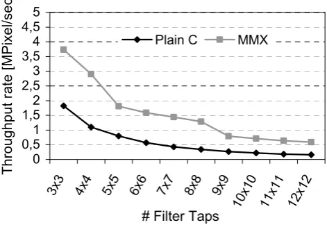
In the following the effects which arise from utilizing the MMX instruction set extensions applied on a 2D-FIR filter with variable coefficients are shown (see Figure 5 and 6). Due to the variable coefficients real multiplication have to be applied. The MMX implementation outperforms the plain C implementation independent of the number of filter taps. One interesting aspect are the discontinutities which can be seen in Figure 6. This is caused by the utilization of the SIMD instruction PMADDWD (packed multiply and add word). The filter window is processed line by line. This instruction is able to handle four 16 bit values at once. Thus, due to the line by line processing mode and the ability to handle four values e.g. a 5x5 filter mask is a disadvantageous case, because one line consists of five values. Due to that, two PMADDWD instructions have to be utilized whereas one PMADDWD instruction calculates just one input sample. Hence, optimal filter windows are multiples of four.
0 0,51 1,52 2,53 3,54 4,55
3x3 4x4 5x5 6x6 7x7 8x8 9x9
10x1 0 11x1 1 12x1 2
# Filter Taps
T
h
roughput rate [M
P
ixel/sec
]
Plain C MMX
1 1,5 2 2,5 3 3,5 4
3x3 4x4 5x5 6x6 7x7 8x8 9x9
10x1 0 11x1 1 12x1 2
# Filter Taps
E
nhanc
ement
Figure 5. Comparison Plain C vs. MMX implementation Figure 6. Enhancement using MMX instructions Optimization Steps
Fig. 4. Optimization steps applied to TI TMS320C6711 and asso-ciated effects.
tion step the execution time decreases which was mainly ac-complished by an improvement of the instruction level par-allelism. This leads to an increase of the power dissipation. However, the consumed energy per sample decreases with each optimization step. This is due to the fact, that the num-ber of achieved output samples per time increases more de-cisively than the power dissipation. The energy per sample is the metric which has to be chosen instead of the power consumption.
2.2 DSP
The TMS320C6711 (TMS320C6711 website) is a high so-phisticated DSP. The underlying processor core is a VLIW-architecture providing eight issue slots. Thus, it is able to execute up to eight different instructions per cycle.
T. von Sydow et al.: Performance analysis 173
0 0,51 1,52 2,53 3,54 4,55
3x3 4x4 5x5 6x6 7x7 8x8 9x9
10x1
0
11x1
1
12x1
2
# Filter Taps
T
h
roughput rate [M
P
ixel/sec
]
Plain C MMX
Fig. 5. Comparison Plain C vs. MMX implementation.
The following optimization steps have been applied: 1. Plain C implementation without any optimization 2. Data type adaptation: Change-over memory data types
to register data types
3. Adaptation of the utilized algorithm (Gupta, Evripidou; 1993)
4. Function inlining
5. Utilization of suitable keywords (e.g. compiler direc-tives, restricted pointer etc.).
As can be seen from Fig. 4 the achieved throughput rate increases with every optimization step. Especially step 4 has been most suitable to gain performance. The energy per sample decreases with every optimization step. The adap-tation of data types has been the outstanding optimization step in terms of reducing energy per sample: Memory data types have been changed in register data types. Thus, unnec-essary memory accesses generally consuming more energy have been avoided.
2.3 GPP with MMX
Due to the high clock speeds and Multimedia Extensions (MMX) modern GPPs are also suitable to meet the high de-mands caused by complex signal processing algorithms. In this work the Pentium MMX in a low power version (Pen-tium website) has been analyzed. In contrast to the proces-sors described before this processor core architecture is based on a superscalar concept.
In the following the effects which arise from utilizing the MMX instruction set extensions applied on a 2D-FIR fil-ter with variable coefficients are shown (see Figs. 5 and 6). Due to the variable coefficients real multiplication have to be applied. The MMX implementation outperforms the plain C implementation independent of the number of filter taps. One interesting aspect are the discontinutities which can be
1 1,5 2 2,5 3 3,5 4
3x3 4x4 5x5 6x6 7x7 8x8 9x9
10x1
0
11x1
1
12x1
2
# Filter Taps
E
nhanc
ement
Fig. 6. Enhancement using MMX instructions.
seen in Fig. 6. This is caused by the utilization of the SIMD instructionP MADDW D (packed multiply and add word). The filter window is processed line by line. This instruction is able to handle four 16 bit values at once. Thus, due to the line by line processing mode and the ability to handle four values, e.g. a 5×5 filter mask is a disadvantageous case, because one line consists of five values. Due to that, two P MADDW Dinstructions have to be utilized whereas one P MADDW Dinstruction calculates just one input sample. Hence, optimal filter windows are multiples of four.
3 Results
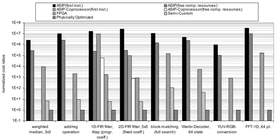
In the following a cost evaluation of all aforementioned pro-grammable architecture blocks concerning different basic operations is presented (see Fig. 7). The costs of other ar-chitecture blocks like FPGAs, physically optimized macros and semi-custom solutions are also depicted in this context. Thus, it is possible to compare different architecture blocks providing different architecture specific characteristics. Con-sidering the energy per sample as well as throughput rate and the required area, the cost function motivated in detail in (Feldk¨amper et al., 2002) was applied here to exemplary basic operations. In this figure the cost ratios between dif-ferent kinds of architecture blocks can be seen. The chosen ASIP is the aforementioned Trimedia.
174 T. von Sydow et al.: Performance analysis
1E-1 1E+0 1E+1 1E+2 1E+3 1E+4 1E+5 1E+6 1E+7 1E+8
weighted median, 3x3
add/reg operation
1D-FIR filter, 4tap (progr.
coeff.)
2D-FIR filter, 5x5 (fixed coeff.)
block-matching (full search)
Viterbi-Decoder, 64 state
YUV-RGB-conversion
FFT-1D, 64 pt.
normalized cost ratios
ASIP(first inst.) ASIP(free comp. resources)
ASIP-Coprocessor(first inst.) ASIP-Coprocessor(free comp. resources)
FPGA Semi-Custom
Physically Optimized
Fig. 7. Exemplary comparison of normalized ATE-cost ratios.
1E+03 1E+04 1E+05 1E+06 1E+07 1E+08 1E+09 1E+10
weighted
median operationadd/reg (progr. coeff.)1D-FIR filter 2D-FIR filter(fixed coeff.) block-matching
nor
m
a
liz
ed c
o
st
s
Celeron 733 MHz ; Plain C (first inst.) Celeron 733 MHz ; MMX/SSE (first inst.) TMS320C6711(first inst.) TMS320C6711(free comp. resources) Trimedia (first inst.) Trimedia(free comp. resources)
Fig. 8. Comparison of cost ratios for programmable processors.
coprocessor structures which are available on the applied Tri-media ASIP. Results for the FIR filter executed on the copro-cessor device lead to minor costs compared to the execution on the ASIP CPU. This example shows what dramatic perfor-mance gains are achievable if programmable processors are integrated together with dedicated and optimized coproces-sor devices. Coprocescoproces-sors can relieve the ASIP CPU in order to attain this valuable resource for other algorithms which re-quire less computational performance but demand for a high degree of flexibility. Considering absolute power consump-tion the total cost ratio between ASIP and physically opti-mized implementation even increases by up to two additional orders of magnitude.
In Fig. 8 the normalized costs are depicted for implemen-tations on the discussed programmable processors including the aforementioned optimization techniques.
Implementations on the DSP architecture TMS320C6711
and the ASIP Trimedia are compared to implementations on the described General Purpose (GP) processor. For the GP processor, it is further differentiated between plain C imple-mentations and optimized software impleimple-mentations apply-ing the MMX coprocessor unit. The implementation costs for the first instantiation of operations differ by up to three orders of magnitude. Several aspects can be emphasized:
– As to be expected, the implementation costs on the GP processor are higher than on the DSP or ASIP architec-ture.
– The MMX unit reduces the implementation costs on a GP processor by about one order of magnitude for those operations they are suited for (e.g. median, FIR filter-ing).
– For both Trimedia and TMS320C6711 the costs be-tween first and second instantiation differ by about 1.5 orders of magnitude.
– The DSP and ASIP implementations differ according to their suitability of the instruction set architecture (ISA) concerning the operation to be performed. For example, the blockmatching operation mainly consists of calcu-lating the sum of pixel differences. This is optimally supported by a Trimedia command (ume8uu). As the TMS320C6711 architecture does not support this type of operation the resulting cost is worse.
4 Conclusions
T. von Sydow et al.: Performance analysis 175 programmable devices yield high throughput rates.
Never-theless, in many cases they are not able to meet the required constraints in terms of e.g. power consumption and through-put rate. As mentioned in the introduction Systems-on-Chip (SoC) will be well-balanced architectures consisting of dif-ferent architecture blocks. In this context due to their inher-ent flexibility programmable architecture blocks will be one integral part of modern SoCs.
It has been shown here, that the ATE cost ratios between different programmable architecture blocks vary up to five orders of magnitude. It is most decisive for the costs how the underlying instruction set and thus the underlying processor architecture matches the requirements of the particular oper-ator. Differences in terms of ATE-costs between dedicated physically optimized macros and programmable devices can amount up to seven orders of magnitude.
References
Blume, H., Feldk¨amper, H., H¨ubert, H., and Noll, T. G.: Analyzing heterogeneous system architectures by means of cost functions: A comparative study for basic operations, Proc. ESSCIRC, pp. 424–427, 2001.
Celeron/Pentium MMX, website, http://www.intel.com
Davis, R., Zhang, N., Camera, K., Chen, F., Markovic, D., Chan, N., Nikolic, B., and Brodersen, R.: A Design Environment for
High-Throughput, Low Power Dedicated Signal Processing Systems, Proc. CICC, pp. 545–548, 2001.
De Hon, A.: The Density Advantage of Configurable Computing, IEEE Computer, pp. 41–49, April 2000.
Feldk¨amper, H., Blume, H., and Noll, T. G.: Study of heterogeneous and reconfigurable architectures in the communication domain, Kleinheubacher Tagung, Oct. 2002.
Feldk¨amper, H. T., Schwann, R., Gierenz, V., and Noll, T. G.: Low Power Delay Calculation for Handheld Ultrasound Beamform-ers, Proc. IEEE Ultrasonics Symposium, 22.–25. October 2000, pp. 1763–1766, 2000.
Gupta, R. and Evripidou, P.: Design and implementation of an effi-cient general-purpose median filter network, Digital Signal Pro-cessing, 3, pp. 64–72, 1993.
Hausner, J. : Integrated Circuits for Next Generation Wireless Sys-tems, Proc. ESSCIRC, pp. 26–29, 2001.
Keutzer, K., Malik, S., Newton, A., Rabaey, J., and Sangiovanni-Vincentelli, A.: System-Level-Design: Orthogonalization of Concerns and Platform-Based Design, IEEE Transaction on Computer-Aided Design of Integrated Circuits and Systems, Vol. 19, No. 12, pp. 1523–1543, Dec. 2000.
Pitas, I. and Venetsanopoulos, A.: Nonlinear Digital Filters, Kluwer, 1990.
TMS320C6711 datasheets, website, http://www.ti.com
Trimedia SDE Documentation Set; 1998, http://www. semiconductors.philips.com/platforms/nexperia/media