Adv. Radio Sci., 4, 251–257, 2006 www.adv-radio-sci.net/4/251/2006/ © Author(s) 2006. This work is licensed under a Creative Commons License.
Advances in
Radio Science
Design and quantitative analysis of parametrisable
eFPGA-architectures for arithmetic
B. Neumann, T. von Sydow, H. Blume, and T. G. Noll
Chair of Electrical Engineering and Computer Systems, RWTH Aachen University, 52062 Aachen, Germany
Abstract. Future SoCs will feature embedded FPGAs (eFPGAs) to enable flexible and efficient implementations of high-throughput digital signal processing applications. Cur-rent research projects on and emerging products containing FPGAs are mainly based on ”standard FPGA”-architectures that are optimised for a very wide range of applications. The implementation costs of these FPGAs are dominated by a very complex interconnect network. This paper presents a method to improve the efficiency of eFPGAs by tailoring them for a certain application domain using a parametrisable architecture template derived from the results of a systematic evaluation of the requirements of the application domain.
Two different architectures are discussed, a reference ar-chitecture to illustrate the methodology and possible optimi-sation measures as well as a specialised arithmetic-oriented eFPGA for applications like correlators, decoders, and fil-ters. For the arithmetic-oriented architecture, a novel logic element (LE) and a special interconnect architecture that was designed with respect to the connectivity characteristics of regular datapaths, are presented. For both architecture tem-plates, physically optimised implementations based on an au-tomatic design approach have been created.
As a first cost comparison of these implementations with standard FPGAs, the LE-density (number of logic elements per mm2)is evaluated. For the arithmetic-oriented architec-ture, the LE-density could be increased by an order of mag-nitude compared to standard architectures.
1 Introduction
The algorithmic complexity of current and future digital sig-nal processing systems leads to an ever growing demand for performance, while short product cycles, mobility and
Correspondence to: B. Neumann
Design and quantitative analysis of parametrisable
eFPGA-architectures for arithmetic
B. Neumann, T. von Sydow, H. Blume, T.G. Noll
Chair of Electrical Engineering and Computer Systems, RWTH Aachen University, 52062 Aachen, Germany
Abstract. Future SoCs will feature embedded FPGAs (eFPGAs) to enable flexible and efficient implementations of high-throughput digital signal processing applications. Current research projects on and emerging products containing FPGAs are mainly based on "standard FPGA"-architectures that are optimised for a very wide range of applications. The implementation costs of these FPGAs are dominated by a very complex interconnect network. This paper presents a method to improve the efficiency of eFPGAs by tailoring them for a certain application domain using a parametrisable architecture template derived from the results of a systematic evaluation of the requirements of the application domain.
Two different architectures are discussed, a reference architecture to illustrate the methodology and possible optimisation measures as well as a specialised arithmetic-oriented eFPGA for applications like correlators, decoders, and filters. For the arithmetic-oriented architecture, a novel logic element (LE) and a special interconnect architecture that was designed with respect to the connectivity characteristics of regular datapaths, are presented. For both architecture templates, physically optimised implemen-tations based on an automatic design approach have been created.
As a first cost comparison of these implementations with standard FPGAs, the LE-density (number of logic elements per mm2) is evaluated. For the arithmetic-oriented archi-tecture, the LE-density could be increased by an order of magnitude compared to standard architectures.
1 Introduction
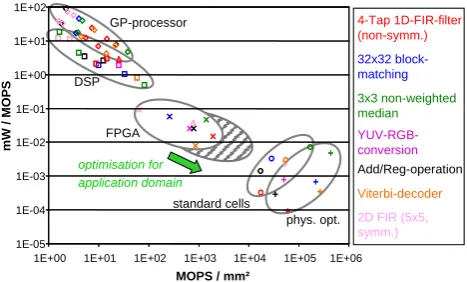
The algorithmic complexity of current and future digital signal processing systems leads to an ever growing demand for performance, while short product cycles, mobility and cost-restrictions make the use of dedicated integrated circuits unfeasible. Fig. 1 illustrates the design space in terms of power efficiency (in mW/MOPS) and area efficiency (in MOPS/mm2) for frequently used digital signal processing tasks implemented on different archi-tectures like general purpose processors, Field Programmable Gate Arrays (FPGAs), physically optimised macros etc. As is well known from Fig. 1, programmable
processor-architectures provide the lowest power- and area efficiency but feature highest flexibility. In contrast, physically optimised macros lead to the highest efficiency, but are inflexible. FPGAs offer an attractive compromise between these two extremes, as they allow for highly parallelised implementations while preserving in-system re-configurability.
MOPS / mm²
1E-05 1E-04 1E-03 1E-02 1E-01 1E+00 1E+01 1E+02
1E+00 1E+01 1E+02 1E+03 1E+04 1E+05 1E+06
mW
/ M
O
PS
32x32 block-matching
3x3 non-weighted median
YUV-RGB-conversion Add/Reg-operation
2D FIR (5x5, symm.)
4-Tap 1D-FIR-filter (non-symm.)
Viterbi-decoder
GP-processor
DSP
FPGA
phys. opt. standard cells
optimisation for application domain
Fig. 1 Design space for different architectures
To meet the contrary demands of today's and future systems, different architecture blocks are integrated on a single chip building a heterogeneous System-on-a-Chip (SoC). A so-called SoC platform addresses a set of applications with similar requirements and characteristics (application domain). This offers the possibility to optimise the included components for this application domain. In the same way the optimisation for an application domain improves the efficiency of a Digital Signal Processor (DSP) over a general purpose CPU, the architecture of an embedded FPGA (eFPGA) can be optimised by designing it for a dedicated application domain. The potential of improvement in efficiency for application domain specific eFPGAs was demonstrated for example in (Neumann et al. 2003) and (Leijten-Nowak et al. 2003). This paper focuses on arithmetic-oriented applications like correlators, decoders and filters, as they promise a high optimisation potential concerning all structural elements of an eFPGA-architecture.
The paper is structured as follows: In section 2, a commonly applied architecture for FPGAs and its char-acteristics concerning area and power dissipation costs is sketched. The properties of eFPGAs specified for an Correspondence to: B. Neumann
Fig. 1. Design space for different architectures.
cost-restrictions make the use of dedicated integrated cir-cuits unfeasible. Fig. 1 illustrates the design space in terms of power efficiency (in mW/MOPS) and area efficiency (in MOPS/mm2) for frequently used digital signal processing tasks implemented on different architectures like general pur-pose processors, Field Programmable Gate Arrays (FPGAs), physically optimised macros etc. As is well known from Fig. 1, programmable processor-architectures provide the lowest power- and area efficiency but feature highest flexi-bility. In contrast, physically optimised macros lead to the highest efficiency, but are inflexible. FPGAs offer an attrac-tive compromise between these two extremes, as they allow for highly parallelised implementations while preserving in-system reconfigurability.
To meet the contrary demands of today’s and future sys-tems, different architecture blocks are integrated on a sin-gle chip building a heterogeneous System-on-a-Chip (SoC). A so-called SoC platform addresses a set of applications with similar requirements and characteristics (application domain). This offers the possibility to optimise the included components for this application domain. In the same way
252 B. Neumann et al.: Design and quantitative analysis of parametrisable eFPGA-architectures 2 B. Neumann et al.: Design and quantitative analysis of parametrisable eFPGA-architectures for arithmetic
arithmetic-oriented application domain are described in section 3. In section 4, the concept of parametrisable eFPGA-architectures is explained and two architecture templates with corresponding implementations are demon-strated. Conclusions are given in section 5.
2 FPGA-architectures
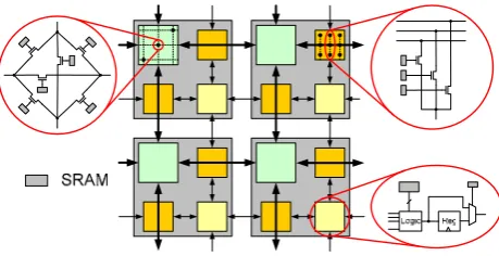
Most common FPGA-architectures, as described e.g. in (Brown et al. 1996), consist of three basic building blocks: Logic Elements (LE), Routing Switches (RS) and Connection Boxes (CB). Fig. 2 shows the architecture of a so-called island-style FPGA-architecture as it was used in the first commercial devices. Most state-of-the-art FPGAs are still based on a modified island-style architectural concept.
Fig. 2 General island-style FPGA-architecture
An LE typically implements basic boolean functionality on bit-level. In most commercial FPGAs, the architecture of an LE is based on one or more lookup-tables (LUTs). A LUT with N inputs shall be called LUT-N in the following. Connection Boxes allow to connect interconnect lines either as in- or outputs of the corresponding LEs. The routing switch provides configurable connections between all its terminals to route signals through the FPGA. Most modern FPGAs use SRAMs to store the configuration information. This allows fast reconfiguration (and in principle dynamic reconfigurability).
To relax the global interconnect requirements, several logic elements can be combined in so-called clusters that share a central connection box. Typically, a cluster consists of about ten LEs. As delays for signals travelling long distances on the FPGA can get significant since they have to pass several routing switches, it is a common technique to provide segmented interconnects with routing lines of different lengths. In this case, certain routing channels skip several routing switches before connecting to another RS. The programmable interconnect features the highest contri-bution to area, power dissipation and delay times of an FPGA. Fig. 3 shows an area- and power breakdown taken from (Kusse et al. 1998) and (George et al. 2001). The figures show that the highest optimisation potential can be expected from the interconnect architecture. It is therefore indispensable to analyse the specific interconnect requirements of the given application domain and hence design the appropriate eFPGA-architecture.
Area 9%
5% 21%
65%
Interconnect LE Clock I/O
Power Dissipation
73% 9%
18%
Interconnect Configuration LE
Fig. 3 FPGA area- and power breakdown
3 Arithmetic-oriented eFPGAs
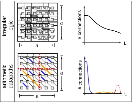
Commercial FPGA components are optimised for a wide range of applications, as they are intended for universal use. Significant research has been conducted in the optimisation of these universal FPGAs, using benchmark circuits from different application domains, e.g. (Betz et al. 1999). An analysis of the logic- and interconnect requirements of arithmetic-datapaths reveals that the architectural require-ments differ significantly from irregular logic. In this contribution, an eFPGA-architecture and the corresponding structural elements have been tailored to an arithmetic-oriented application domain. Considering the interconnect requirements of different applications mapped to FPGAs, it is useful to consider the histogram of the lengths of allocated interconnections. Fig. 4 shows such a qualitative histogram of the allocated connections between logic elements. For irregular logic, the number of connections between the LEs decreases with the connection length L. Arithmetic-datapaths, however, have a very high locality, hence exposing a peak in the distribution for short connections. Only few lines of intermediate length are re-quired, while some long connections, usually representing broadcast lines, are used.
irre
gula
r
logic
a
a
L
# co
nn
ec
ti
o
n
s
arithmeti
c
datapath
s
a
a
# c
o
nnectio
n
s
L
Fig. 4 Application domain specific routing requirements
To confirm this qualitative histogram, an investigation of the allocated routing resources in a commercial FPGA device has been conducted. For this purpose, key compo-nents of a GPS-receiver (Global Positioning System) have been implemented on an Altera Stratix device (Kappen et al. 2006). Using the corresponding design software, the num-ber of allocated routing resources according to their seg-Fig. 2. General island-style FPGA-architecture.
the optimisation for an application domain improves the ef-ficiency of a Digital Signal Processor (DSP) over a gen-eral purpose CPU, the architecture of an embedded FPGA (eFPGA) can be optimised by designing it for a dedicated ap-plication domain. The potential of improvement in efficiency for application domain specific eFPGAs was demonstrated for example in Neumann et al. (2003) and Leijten-Nowak et al. (2003). This paper focuses on arithmetic-oriented appli-cations like correlators, decoders and filters, as they promise a high optimisation potential concerning all structural ele-ments of an eFPGA-architecture.
The paper is structured as follows: In Sect. 2, a commonly applied architecture for FPGAs and its characteristics con-cerning area and power dissipation costs is sketched. The properties of eFPGAs specified for an arithmetic-oriented ap-plication domain are described in Sect. 3. In Sect. 4, the con-cept of parametrisable eFPGA-architectures is explained and two architecture templates with corresponding implementa-tions are demonstrated. Conclusions are given in Sect. 5.
2 FPGA-architectures
Most common FPGA-architectures, as described e.g. in Brown et al. (1996), consist of three basic building blocks: Logic Elements (LE), Routing Switches (RS) and Connec-tion Boxes (CB). Figure 2 shows the architecture of a so-called island-style FPGA-architecture as it was used in the first commercial devices. Most state-of-the-art FPGAs are still based on a modified island-style architectural concept.
An LE typically implements basic boolean functionality on bit-level. In most commercial FPGAs, the architecture of an LE is based on one or more lookup-tables (LUTs). A LUT withN inputs shall be called LUT-N in the follow-ing. Connection Boxes allow to connect interconnect lines either as in- or outputs of the corresponding LEs. The rout-ing switch provides configurable connections between all its terminals to route signals through the FPGA. Most modern FPGAs use SRAMs to store the configuration information. This allows fast reconfiguration (and in principle dynamic reconfigurability).
2 B. Neumann et al.: Design and quantitative analysis of parametrisable eFPGA-architectures for arithmetic
arithmetic-oriented application domain are described in section 3. In section 4, the concept of parametrisable eFPGA-architectures is explained and two architecture templates with corresponding implementations are demon-strated. Conclusions are given in section 5.
2 FPGA-architectures
Most common FPGA-architectures, as described e.g. in (Brown et al. 1996), consist of three basic building blocks: Logic Elements (LE), Routing Switches (RS) and Connection Boxes (CB). Fig. 2 shows the architecture of a so-called island-style FPGA-architecture as it was used in the first commercial devices. Most state-of-the-art FPGAs are still based on a modified island-style architectural concept.
Fig. 2 General island-style FPGA-architecture
An LE typically implements basic boolean functionality on bit-level. In most commercial FPGAs, the architecture of an LE is based on one or more lookup-tables (LUTs). A LUT with N inputs shall be called LUT-N in the following. Connection Boxes allow to connect interconnect lines either as in- or outputs of the corresponding LEs. The routing switch provides configurable connections between all its terminals to route signals through the FPGA. Most modern FPGAs use SRAMs to store the configuration information. This allows fast reconfiguration (and in principle dynamic reconfigurability).
To relax the global interconnect requirements, several logic elements can be combined in so-called clusters that share a central connection box. Typically, a cluster consists of about ten LEs. As delays for signals travelling long distances on the FPGA can get significant since they have to pass several routing switches, it is a common technique to provide segmented interconnects with routing lines of different lengths. In this case, certain routing channels skip several routing switches before connecting to another RS. The programmable interconnect features the highest contri-bution to area, power dissipation and delay times of an FPGA. Fig. 3 shows an area- and power breakdown taken from (Kusse et al. 1998) and (George et al. 2001). The figures show that the highest optimisation potential can be expected from the interconnect architecture. It is therefore indispensable to analyse the specific interconnect requirements of the given application domain and hence design the appropriate eFPGA-architecture.
Area
9%
5% 21%
65% Interconnect LE Clock I/O
Power Dissipation
73% 9%
18%
Interconnect Configuration LE
Fig. 3 FPGA area- and power breakdown
3 Arithmetic-oriented eFPGAs
Commercial FPGA components are optimised for a wide range of applications, as they are intended for universal use. Significant research has been conducted in the optimisation of these universal FPGAs, using benchmark circuits from different application domains, e.g. (Betz et al. 1999). An analysis of the logic- and interconnect requirements of arithmetic-datapaths reveals that the architectural require-ments differ significantly from irregular logic. In this contribution, an eFPGA-architecture and the corresponding structural elements have been tailored to an arithmetic-oriented application domain. Considering the interconnect requirements of different applications mapped to FPGAs, it is useful to consider the histogram of the lengths of allocated interconnections. Fig. 4 shows such a qualitative histogram of the allocated connections between logic elements. For irregular logic, the number of connections between the LEs decreases with the connection length L. Arithmetic-datapaths, however, have a very high locality, hence exposing a peak in the distribution for short connections. Only few lines of intermediate length are re-quired, while some long connections, usually representing broadcast lines, are used.
irre
gula
r
logic
a
a
L
# co
nn
ec
ti
o
n
s
arithmeti
c
datapath
s
a
a
# c
o
nnectio
n
s
L
Fig. 4 Application domain specific routing requirements
To confirm this qualitative histogram, an investigation of the allocated routing resources in a commercial FPGA device has been conducted. For this purpose, key compo-nents of a GPS-receiver (Global Positioning System) have been implemented on an Altera Stratix device (Kappen et al. 2006). Using the corresponding design software, the num-Fig. 3. FPGA area- and power breakdown.
To relax the global interconnect requirements, several logic elements can be combined in so-called clusters that share a central connection box. Typically, a cluster consists of about ten LEs. As delays for signals travelling long dis-tances on the FPGA can get significant since they have to pass several routing switches, it is a common technique to provide segmented interconnects with routing lines of differ-ent lengths. In this case, certain routing channels skip several routing switches before connecting to another RS.
The programmable interconnect features the highest con-tribution to area, power dissipation and delay times of an FPGA. Figure 3 shows an area- and power breakdown taken from Kusse et al. (1998) and George et al. (2001). The figures show that the highest optimisation potential can be expected from the interconnect architecture. It is therefore indispens-able to analyse the specific interconnect requirements of the given application domain and hence design the appropriate eFPGA-architecture.
3 Arithmetic-oriented eFPGAs
Commercial FPGA components are optimised for a wide range of applications, as they are intended for universal use. Significant research has been conducted in the optimisation of these universal FPGAs, using benchmark circuits from dif-ferent application domains (e.g. Betz et al., 1999). An analy-sis of the logic- and interconnect requirements of arithmetic-datapaths reveals that the architectural requirements differ significantly from irregular logic. In this contribution, an eFPGA-architecture and the corresponding structural ele-ments have been tailored to an arithmetic-oriented applica-tion domain. Considering the interconnect requirements of different applications mapped to FPGAs, it is useful to con-sider the histogram of the lengths of allocated interconnec-tions. Fig. 4 shows such a qualitative histogram of the al-located connections between logic elements. For irregular logic, the number of connections between the LEs decreases with the connection length L. Arithmetic-datapaths, however, have a very high locality, hence exposing a peak in the distri-bution for short connections. Only few lines of intermediate length are required, while some long connections, usually representing broadcast lines, are used.
To confirm this qualitative histogram, an investigation of the allocated routing resources in a commercial FPGA
B. Neumann et al.: Design and quantitative analysis of parametrisable eFPGA-architectures 253 arithmetic-oriented application domain are described in
section 3. In section 4, the concept of parametrisable eFPGA-architectures is explained and two architecture templates with corresponding implementations are demon-strated. Conclusions are given in section 5.
2 FPGA-architectures
Most common FPGA-architectures, as described e.g. in (Brown et al. 1996), consist of three basic building blocks: Logic Elements (LE), Routing Switches (RS) and Connection Boxes (CB). Fig. 2 shows the architecture of a so-called island-style FPGA-architecture as it was used in the first commercial devices. Most state-of-the-art FPGAs are still based on a modified island-style architectural concept.
Fig. 2 General island-style FPGA-architecture
An LE typically implements basic boolean functionality on bit-level. In most commercial FPGAs, the architecture of an LE is based on one or more lookup-tables (LUTs). A LUT with N inputs shall be called LUT-N in the following. Connection Boxes allow to connect interconnect lines either as in- or outputs of the corresponding LEs. The routing switch provides configurable connections between all its terminals to route signals through the FPGA. Most modern FPGAs use SRAMs to store the configuration information. This allows fast reconfiguration (and in principle dynamic reconfigurability).
To relax the global interconnect requirements, several logic elements can be combined in so-called clusters that share a central connection box. Typically, a cluster consists of about ten LEs. As delays for signals travelling long distances on the FPGA can get significant since they have to pass several routing switches, it is a common technique to provide segmented interconnects with routing lines of different lengths. In this case, certain routing channels skip several routing switches before connecting to another RS. The programmable interconnect features the highest contri-bution to area, power dissipation and delay times of an FPGA. Fig. 3 shows an area- and power breakdown taken from (Kusse et al. 1998) and (George et al. 2001). The figures show that the highest optimisation potential can be expected from the interconnect architecture. It is therefore indispensable to analyse the specific interconnect requirements of the given application domain and hence design the appropriate eFPGA-architecture.
Area
9%
5% 21%
65%
Interconnect LE Clock I/O
Power Dissipation
73% 9%
18%
Interconnect Configuration LE
Fig. 3 FPGA area- and power breakdown
3 Arithmetic-oriented eFPGAs
Commercial FPGA components are optimised for a wide range of applications, as they are intended for universal use. Significant research has been conducted in the optimisation of these universal FPGAs, using benchmark circuits from different application domains, e.g. (Betz et al. 1999). An analysis of the logic- and interconnect requirements of arithmetic-datapaths reveals that the architectural require-ments differ significantly from irregular logic. In this contribution, an eFPGA-architecture and the corresponding structural elements have been tailored to an arithmetic-oriented application domain. Considering the interconnect requirements of different applications mapped to FPGAs, it is useful to consider the histogram of the lengths of allocated interconnections. Fig. 4 shows such a qualitative histogram of the allocated connections between logic elements. For irregular logic, the number of connections between the LEs decreases with the connection length L. Arithmetic-datapaths, however, have a very high locality, hence exposing a peak in the distribution for short connections. Only few lines of intermediate length are re-quired, while some long connections, usually representing broadcast lines, are used.
irre
gula
r
logic
a
a
L
# co
nn
ec
ti
o
n
s
arithmeti
c
datapath
s
a
a
# c
o
nnectio
n
s
L
Fig. 4 Application domain specific routing requirements
To confirm this qualitative histogram, an investigation of the allocated routing resources in a commercial FPGA device has been conducted. For this purpose, key compo-nents of a GPS-receiver (Global Positioning System) have been implemented on an Altera Stratix device (Kappen et al. 2006). Using the corresponding design software, the num-ber of allocated routing resources according to their seg-Fig. 4. Application domain specific routing requirements.
vice has been conducted. For this purpose, key components of a GPS-receiver (Global Positioning System) have been im-plemented on an Altera Stratix device (Kappen et al. 2006). Using the corresponding design software, the number of al-located routing resources according to their segment length has been determined. Figure 5 shows the results for two ex-emplary components, the correlator and the corresponding control logic. While the irregular control logic has a high fraction of intermediate segments and considerably less short and long segments, the correlator logic itself has a significant amount of direct nearest-neighbour connections. Since the overhead in the interconnect architecture of today’s FPGAs is mainly due to their high flexibility, a considerable reduc-tion of this overhead can be expected if the architecture is tailored to this application domain.
A further reduction can be achieved by carefully designing the logic elements to preserve the communication locality of arithmetic datapaths. In order to relax the interconnect re-quirements, appropriate dedicated logic and connections are provided in the LEs. A basic example is the use of dedicated carry-chains in commercial FPGAs. Direct connections be-tween the LEs enable the use of adders with no additional routing involved in the carry-propagation.
Additional optimisation can be achieved if the LEs are de-signed such that frequently used basic operations of typical datapaths are directly mapped to one LE or LE cluster re-spectively. An example of optimising the LE architecture in that sense is to provide the possibility of realising a gated full-addition efficiently within one LE, as gated full-addition is a common part of many arithmetic-oriented applications (multiply, etc.). In the same way, other dedicated logic and dedicated interconnect can be employed to improve the effi-ciency of the architecture. For example, while typical logic elements feature one register, arithmetic datapaths with ex-tensive pipelining require significantly more registers per LE.
B. Neumann et al.: Design and quantitative analysis of parametrisable eFPGA-architectures for arithmetic 3
ment length has been determined. Fig. 5 shows the results for two exemplary components, the correlator and the corresponding control logic. While the irregular control logic has a high fraction of intermediate segments and considerably less short and long segments, the correlator logic itself has a significant amount of direct nearest-neighbour connections. Since the overhead in the interconnect architecture of today's FPGAs is mainly due to their high flexibility, a considerable reduction of this overhead can be expected if the architecture is tailored to this application domain.
Correlator-control
57%
21% 22%
long medium short
Correlator
13%
69%
18%
long medium short
Fig. 5 Allocated interconnect lengths for irregular logic and arithmetic
A further reduction can be achieved by carefully designing the logic elements to preserve the communication locality of arithmetic datapaths. In order to relax the interconnect requirements, appropriate dedicated logic and connections are provided in the LEs. A basic example is the use of dedicated carry-chains in commercial FPGAs. Direct connections between the LEs enable the use of adders with no additional routing involved in the carry-propagation. Additional optimisation can be achieved if the LEs are designed such that frequently used basic operations of typical datapaths are directly mapped to one LE or LE cluster respectively. An example of optimising the LE architecture in that sense is to provide the possibility of realising a gated full-addition efficiently within one LE, as gated full-addition is a common part of many arithmetic-oriented applications (multiply, etc.). In the same way, other dedicated logic and dedicated interconnect can be employed to improve the efficiency of the architecture. For example, while typical logic elements feature one register, arithmetic datapaths with extensive pipelining require significantly more registers per LE.
4 Parametrisable eFPGA-architectures
In the following section, the design flow applied in this contribution is presented. This flow is based on an architecture template of the eFPGA with adjustable parameters. From this template, physically optimised realisations of the macro are created.
4.1 Layout automation and parameters
The basic design concept is based on generic architecture templates which are parametrisable in a wide range and a couple of physically optimised so-called leafcells. An auto-matic layout generation using a flexible datapath generator as described in (Weiss et al. 2001) is used to generate the layout of the eFPGA-macro. Table 1 lists some exemplary
parameters influencing the basic structural elements of an eFPGA-architecture.
LE no. of in- /outputs
amount of dedicated logic Cluster no. and alignment of LEs
no. of in- /outputs Interconnect no. of hierarchy levels
size of routing channels
segmentation of routing channels flexibility
Configuration no. of parallel configuration sets no. of shared configuration sets
Others granularity of supply and clock domains
Table 1 Exemplary architectural parameters
These parameters feature strong interdependencies. For example, the architecture of the LE and the number of in- and outputs have a strong impact on the interconnect architecture.
In the present work, the design of a physically optimised layout for a parametrisable architecture is based on the following steps:
An architecture template has been conceived and realised in form of a generic structural description. A small set of key components like logic elements and switch points used for routing switches has been designed. After adjusting all required parameters of the architecture template, a physi-cally optimised macro is generated automatiphysi-cally applying the datapath generator. After the netlist extraction of this macro and setting up the simulation environment, a detailed timing and power analysis can be performed. If design constraints are not met, parameters can be easily adapted within the generic description and the macro generation process can be initiated again. The cycle time of adjusting parameters and acquiring cost and performance values depends on the complexity of the target macro.
4.2 Reference architecture
The first architecture template which has been realised serves as reference (Fig. 6). The interconnect architecture of this reference is based on the interconnect structure of modern commercial devices (Website Altera, Website Xilinx). A local connection box (CB 0 in Fig. 6) provides the connection between LEs arranged as clusters and the global connection box (CB 1 in Fig. 6). The global CB provides the connection to the global routing lines. Routing of signals coming from the global connection lines is exe-cuted by the RS. There are two types of routing switches: the first types enables regular vertical and horizontal rout-ing between neighbourrout-ing RS, the second type is enhanced and offers the possibility of segmented routing for certain lines. Adaptable parameters of the corresponding architec-ture template are for example the number of routing tracks, the number of clusters per CB and the length of intercon-nect lines for the segmented routing.
Fig. 5. Allocated interconnect lengths for irregular logic and
arith-metic.
Table 1. Exemplary architectural parameters.
LE no. of in- /outputs amount of dedicated logic Cluster no. and alignment of LEs
no. of in- /outputs Interconnect no. of hierarchy levels
size of routing channels
segmentation of routing channels flexibility
Configuration no. of parallel configuration sets no. of shared configuration sets Others granularity of supply and clock domains
4 Parametrisable eFPGA-architectures
In the following section, the design flow applied in this con-tribution is presented. This flow is based on an architecture template of the eFPGA with adjustable parameters. From this template, physically optimised realisations of the macro are created.
4.1 Layout automation and parameters
The basic design concept is based on generic architecture templates which are parametrisable in a wide range and a couple of physically optimised so-called leafcells. An auto-matic layout generation using a flexible datapath generator as described in (Weiss et al. 2001) is used to generate the layout of the eFPGA-macro. Table 1 lists some exemplary param-eters influencing the basic structural elements of an eFPGA-architecture.
These parameters feature strong interdependencies. For example, the architecture of the LE and the number of in- and outputs have a strong impact on the interconnect architecture. In the present work, the design of a physically optimised layout for a parametrisable architecture is based on the fol-lowing steps:
An architecture template has been conceived and realised in form of a generic structural description. A small set of key components like logic elements and switch points used for
254 B. Neumann et al.: Design and quantitative analysis of parametrisable eFPGA-architectures
4
B. Neumann et al.: Design and quantitative analysis of parametrisable eFPGA-architectures for arithmetic
Cluster
LECB 0 LE LE LE CB 1
...
RS Cluster RS RSFig. 6
Hierarchical reference architecture
The LE architecture unlike commercial devices has been
designed for arithmetic-oriented applications and is based
on dedicated logic without employing LUTs (Fig. 7). Gated
full-addition, add-compare-select and other arithmetic
operations can be implemented very efficiently. In
particular, the second register allows for efficient
imple-mentation of pipelined datapaths. The logic complexity of
the LE is smaller than for a LUT with the same number of
inputs. The number of SRAM-cells and hence overall
silicon area required for this LE is much smaller than a
LUT-based solution.
Fig. 7
LE of reference architecture
Applying the design flow mentioned above, several macros
with different parameter settings have been designed in a
180nm-technology. Two exemplary macros featuring
different cluster sizes, different number of LEs per macro
and different number and segmentation of routing tracks
are depicted in Fig. 8.
RS CB
c
256 LEs
4x4 LEs per global CB
52 tracks length1
14 tracks length 2
d
1024 LEs
2x4 LEs pro global CB
12 tracks length1
tracks length 2 (hor.)
6 tracks length 4 (ver.)
Fig. 8
Reference architecture macros and corresponding
For the local CB (CB0 in Fig. 6) a detailed analysis of
flexibility requirements has been conducted using a variety
of exemplary basic operations. Fig. 9 shows the area
fraction of the LEs proportional to the complete macro for
different levels of connection box flexibility. The flexibility
of the complete architecture is determined by the number of
possible connections within a CB. At first, the interconnect
of the local CB has been designed for simple arithmetic
datapaths (e.g. gated full addition, carry-ripple addition
etc.). This means that only those connections are realised
which are required for ADD/MULT operations. Such a
restricted CB would mean that other types of operations
cannot be performed with this CB configuration. In the next
steps, the interconnect structure has been enhanced in a
way that multiplexer functionality and randomised logic
can be implemented (step 2, 3 and 4).
In the following step, more complex arithmetic datapaths
have been included (e.g. carry-save arithmetic, CSA). The
reference point in this depiction corresponds to the full
flexible solution (rightmost bars). Above the diagram, the
according layouts of the CB, which are created
automatically, are shown. The area fraction of the LEs is
directly influenced by the routing parameters described
above. Macro
1 includes more global routing tracks.
Therefore, this solution features a higher flexibility than
macro
2 which has got a more restricted routing
architecture. The area of the LE and the local CB is the
same for both macros.
0,0 2,0 4,0 6,0 8,0 10,0 12,0 14,0 16,0
ADD/MULT + MUX + (N)AND2, (N)OR2, X(N)OR2
+ random-logic
+ CSA + full flexibility are a fr act io n L E in %
hierarch. eFPGA-macro 1 (256 LEs) hierarch. eFPGA-macro 2 (1024 LEs) 0,0 2,0 4,0 6,0 8,0 10,0 12,0 14,0 16,0
ADD/MULT + MUX + (N)AND2, (N)OR2, X(N)OR2
+ random-logic
+ CSA + full flexibility are a fr act io n L E in %
hierarch. eFPGA-macro 1 (256 LEs) hierarch. eFPGA-macro 2 (1024 LEs) additional
functionality
Fig. 9
Interrelation of flexibility and area within CB0
For this first architecture template, the routing architecture
is still the dominating factor in terms of area, timing and
power consumption. Using the design methodology (see
4.1) established with the reference architecture, an
eFPGA-architecture tailored for an arithmetic-oriented application
domain has been developed.
4.3
Arithmetic-oriented eFPGA-architecture
The requirements of arithmetic-oriented datapaths have
been addressed by the eFPGA architecture described in the
following. The architecture uses arithmetic-oriented LEs
that are connected as two-dimensional clusters, reflecting
Fig. 6. Hierarchical reference architecture.
4 B. Neumann et al.: Design and quantitative analysis of parametrisable eFPGA-architectures for arithmetic
Cluster LE CB 0 LE LE LE CB 1
...
RS Cluster RS RSFig. 6 Hierarchical reference architecture
The LE architecture unlike commercial devices has been designed for arithmetic-oriented applications and is based on dedicated logic without employing LUTs (Fig. 7). Gated full-addition, add-compare-select and other arithmetic operations can be implemented very efficiently. In particular, the second register allows for efficient imple-mentation of pipelined datapaths. The logic complexity of the LE is smaller than for a LUT with the same number of inputs. The number of SRAM-cells and hence overall silicon area required for this LE is much smaller than a LUT-based solution.
Fig. 7 LE of reference architecture
Applying the design flow mentioned above, several macros with different parameter settings have been designed in a 180nm-technology. Two exemplary macros featuring different cluster sizes, different number of LEs per macro and different number and segmentation of routing tracks are depicted in Fig. 8.
RS CB
c 256 LEs
4x4 LEs per global CB
52 tracks length1
14 tracks length 2 d
1024 LEs
2x4 LEs pro global CB
12 tracks length1
tracks length 2 (hor.)
6 tracks length 4 (ver.)
Fig. 8 Reference architecture macros and corresponding parameter settings
For the local CB (CB0 in Fig. 6) a detailed analysis of flexibility requirements has been conducted using a variety of exemplary basic operations. Fig. 9 shows the area fraction of the LEs proportional to the complete macro for different levels of connection box flexibility. The flexibility of the complete architecture is determined by the number of possible connections within a CB. At first, the interconnect of the local CB has been designed for simple arithmetic datapaths (e.g. gated full addition, carry-ripple addition etc.). This means that only those connections are realised which are required for ADD/MULT operations. Such a restricted CB would mean that other types of operations cannot be performed with this CB configuration. In the next steps, the interconnect structure has been enhanced in a way that multiplexer functionality and randomised logic can be implemented (step 2, 3 and 4).
In the following step, more complex arithmetic datapaths have been included (e.g. carry-save arithmetic, CSA). The reference point in this depiction corresponds to the full flexible solution (rightmost bars). Above the diagram, the according layouts of the CB, which are created automatically, are shown. The area fraction of the LEs is directly influenced by the routing parameters described above. Macro 1 includes more global routing tracks. Therefore, this solution features a higher flexibility than macro 2 which has got a more restricted routing architecture. The area of the LE and the local CB is the same for both macros.
0,0 2,0 4,0 6,0 8,0 10,0 12,0 14,0 16,0
ADD/MULT + MUX + (N)AND2,
(N)OR2, X(N)OR2
+ random-logic
+ CSA + full
flexibility are a fr act io n L E in %
hierarch. eFPGA-macro 1 (256 LEs) hierarch. eFPGA-macro 2 (1024 LEs)
0,0 2,0 4,0 6,0 8,0 10,0 12,0 14,0 16,0
ADD/MULT + MUX + (N)AND2,
(N)OR2, X(N)OR2
+ random-logic
+ CSA + full
flexibility are a fr act io n L E in %
hierarch. eFPGA-macro 1 (256 LEs) hierarch. eFPGA-macro 2 (1024 LEs)
additional functionality
Fig. 9 Interrelation of flexibility and area within CB0
For this first architecture template, the routing architecture is still the dominating factor in terms of area, timing and power consumption. Using the design methodology (see 4.1) established with the reference architecture, an eFPGA-architecture tailored for an arithmetic-oriented application domain has been developed.
4.3 Arithmetic-oriented eFPGA-architecture
The requirements of arithmetic-oriented datapaths have been addressed by the eFPGA architecture described in the following. The architecture uses arithmetic-oriented LEs that are connected as two-dimensional clusters, reflecting the typical orientation of processing elements in filters and Fig. 7. LE of reference architecture.
routing switches has been designed. After adjusting all re-quired parameters of the architecture template, a physically optimised macro is generated automatically applying the dat-apath generator. After the netlist extraction of this macro and setting up the simulation environment, a detailed timing and power analysis can be performed. If design constraints are not met, parameters can be easily adapted within the generic description and the macro generation process can be initiated again. The cycle time of adjusting parameters and acquiring cost and performance values depends on the complexity of the target macro.
4.2 Reference architecture
The first architecture template which has been realised serves as reference (Fig. 6). The interconnect architecture of this reference is based on the interconnect structure of modern commercial devices (Website Altera, Website Xilinx). A lo-cal connection box (CB 0 in Fig. 6) provides the connection between LEs arranged as clusters and the global connection box (CB 1 in Fig. 6). The global CB provides the connection to the global routing lines. Routing of signals coming from
4 B. Neumann et al.: Design and quantitative analysis of parametrisable eFPGA-architectures for arithmetic
Cluster LE CB 0 LE LE LE CB 1
...
RS Cluster RS RSFig. 6 Hierarchical reference architecture
The LE architecture unlike commercial devices has been designed for arithmetic-oriented applications and is based on dedicated logic without employing LUTs (Fig. 7). Gated full-addition, add-compare-select and other arithmetic operations can be implemented very efficiently. In particular, the second register allows for efficient imple-mentation of pipelined datapaths. The logic complexity of the LE is smaller than for a LUT with the same number of inputs. The number of SRAM-cells and hence overall silicon area required for this LE is much smaller than a LUT-based solution.
Fig. 7 LE of reference architecture
Applying the design flow mentioned above, several macros with different parameter settings have been designed in a 180nm-technology. Two exemplary macros featuring different cluster sizes, different number of LEs per macro and different number and segmentation of routing tracks are depicted in Fig. 8.
RS CB
c 256 LEs
4x4 LEs per global CB
52 tracks length1
14 tracks length 2 d
1024 LEs
2x4 LEs pro global CB
12 tracks length1
tracks length 2 (hor.)
6 tracks length 4 (ver.)
Fig. 8 Reference architecture macros and corresponding parameter settings
For the local CB (CB0 in Fig. 6) a detailed analysis of flexibility requirements has been conducted using a variety of exemplary basic operations. Fig. 9 shows the area fraction of the LEs proportional to the complete macro for different levels of connection box flexibility. The flexibility of the complete architecture is determined by the number of possible connections within a CB. At first, the interconnect of the local CB has been designed for simple arithmetic datapaths (e.g. gated full addition, carry-ripple addition etc.). This means that only those connections are realised which are required for ADD/MULT operations. Such a restricted CB would mean that other types of operations cannot be performed with this CB configuration. In the next steps, the interconnect structure has been enhanced in a way that multiplexer functionality and randomised logic can be implemented (step 2, 3 and 4).
In the following step, more complex arithmetic datapaths have been included (e.g. carry-save arithmetic, CSA). The reference point in this depiction corresponds to the full flexible solution (rightmost bars). Above the diagram, the according layouts of the CB, which are created automatically, are shown. The area fraction of the LEs is directly influenced by the routing parameters described above. Macro 1 includes more global routing tracks. Therefore, this solution features a higher flexibility than macro 2 which has got a more restricted routing architecture. The area of the LE and the local CB is the same for both macros.
0,0 2,0 4,0 6,0 8,0 10,0 12,0 14,0 16,0
ADD/MULT + MUX + (N)AND2,
(N)OR2, X(N)OR2
+ random-logic
+ CSA + full
flexibility are a fr act io n L E in %
hierarch. eFPGA-macro 1 (256 LEs) hierarch. eFPGA-macro 2 (1024 LEs)
0,0 2,0 4,0 6,0 8,0 10,0 12,0 14,0 16,0
ADD/MULT + MUX + (N)AND2,
(N)OR2, X(N)OR2
+ random-logic
+ CSA + full
flexibility are a fr act io n L E in %
hierarch. eFPGA-macro 1 (256 LEs) hierarch. eFPGA-macro 2 (1024 LEs)
additional functionality
Fig. 9 Interrelation of flexibility and area within CB0
For this first architecture template, the routing architecture is still the dominating factor in terms of area, timing and power consumption. Using the design methodology (see 4.1) established with the reference architecture, an eFPGA-architecture tailored for an arithmetic-oriented application domain has been developed.
4.3 Arithmetic-oriented eFPGA-architecture
The requirements of arithmetic-oriented datapaths have been addressed by the eFPGA architecture described in the following. The architecture uses arithmetic-oriented LEs that are connected as two-dimensional clusters, reflecting the typical orientation of processing elements in filters and Fig. 8. Reference architecture macros and corresponding parameter
settings.
4 B. Neumann et al.: Design and quantitative analysis of parametrisable eFPGA-architectures for arithmetic
Cluster LE CB 0 LE LE LE CB 1
...
RS Cluster RS RSFig. 6 Hierarchical reference architecture
The LE architecture unlike commercial devices has been designed for arithmetic-oriented applications and is based on dedicated logic without employing LUTs (Fig. 7). Gated full-addition, add-compare-select and other arithmetic operations can be implemented very efficiently. In particular, the second register allows for efficient imple-mentation of pipelined datapaths. The logic complexity of the LE is smaller than for a LUT with the same number of inputs. The number of SRAM-cells and hence overall silicon area required for this LE is much smaller than a LUT-based solution.
Fig. 7 LE of reference architecture
Applying the design flow mentioned above, several macros with different parameter settings have been designed in a 180nm-technology. Two exemplary macros featuring different cluster sizes, different number of LEs per macro and different number and segmentation of routing tracks are depicted in Fig. 8.
RS CB
c 256 LEs
4x4 LEs per global CB 52 tracks length1 14 tracks length 2
d
1024 LEs
2x4 LEs pro global CB 12 tracks length1 tracks length 2 (hor.) 6 tracks length 4 (ver.)
Fig. 8 Reference architecture macros and corresponding parameter settings
For the local CB (CB0 in Fig. 6) a detailed analysis of flexibility requirements has been conducted using a variety of exemplary basic operations. Fig. 9 shows the area fraction of the LEs proportional to the complete macro for different levels of connection box flexibility. The flexibility of the complete architecture is determined by the number of possible connections within a CB. At first, the interconnect of the local CB has been designed for simple arithmetic datapaths (e.g. gated full addition, carry-ripple addition etc.). This means that only those connections are realised which are required for ADD/MULT operations. Such a restricted CB would mean that other types of operations cannot be performed with this CB configuration. In the next steps, the interconnect structure has been enhanced in a way that multiplexer functionality and randomised logic can be implemented (step 2, 3 and 4).
In the following step, more complex arithmetic datapaths have been included (e.g. carry-save arithmetic, CSA). The reference point in this depiction corresponds to the full flexible solution (rightmost bars). Above the diagram, the according layouts of the CB, which are created automatically, are shown. The area fraction of the LEs is directly influenced by the routing parameters described above. Macro 1 includes more global routing tracks. Therefore, this solution features a higher flexibility than macro 2 which has got a more restricted routing architecture. The area of the LE and the local CB is the same for both macros.
0,0 2,0 4,0 6,0 8,0 10,0 12,0 14,0 16,0
ADD/MULT + MUX + (N)AND2,
(N)OR2, X(N)OR2
+ random-logic
+ CSA + full
flexibility are a fr act io n L E in %
hierarch. eFPGA-macro 1 (256 LEs) hierarch. eFPGA-macro 2 (1024 LEs)
0,0 2,0 4,0 6,0 8,0 10,0 12,0 14,0 16,0
ADD/MULT + MUX + (N)AND2,
(N)OR2, X(N)OR2
+ random-logic
+ CSA + full
flexibility are a fr act io n L E in %
hierarch. eFPGA-macro 1 (256 LEs) hierarch. eFPGA-macro 2 (1024 LEs)
additional functionality
Fig. 9 Interrelation of flexibility and area within CB0
For this first architecture template, the routing architecture is still the dominating factor in terms of area, timing and power consumption. Using the design methodology (see 4.1) established with the reference architecture, an eFPGA-architecture tailored for an arithmetic-oriented application domain has been developed.
4.3 Arithmetic-oriented eFPGA-architecture
The requirements of arithmetic-oriented datapaths have been addressed by the eFPGA architecture described in the following. The architecture uses arithmetic-oriented LEs that are connected as two-dimensional clusters, reflecting the typical orientation of processing elements in filters and
Fig. 9. Interrelation of flexibility and area within CBO.
the global connection lines is executed by the RS. There are two types of routing switches: the first types enables regu-lar vertical and horizontal routing between neighbouring RS, the second type is enhanced and offers the possibility of seg-mented routing for certain lines. Adaptable parameters of the corresponding architecture template are for example the number of routing tracks, the number of clusters per CB and the length of interconnect lines for the segmented routing.
The LE architecture unlike commercial devices has been designed for arithmetic-oriented applications and is based on dedicated logic without employing LUTs (Fig. 7). Gated full-addition, add-compare-select and other arithmetic op-erations can be implemented very efficiently. In particu-lar, the second register allows for efficient implementation of pipelined datapaths. The logic complexity of the LE is smaller than for a LUT with the same number of inputs. The number of SRAM-cells and hence overall silicon area required for this LE is much smaller than a LUT-based solu-tion.
B. Neumann et al.: Design and quantitative analysis of parametrisable eFPGA-architectures 255
B. Neumann et al.: Design and quantitative analysis of parametrisable eFPGA-architectures for arithmetic
5
multipliers. The LEs are connected with a directional
near-est-neighbour interconnect. Rather than providing random
connections to all surrounding neighbours, this structure
reflects the typical nature of arithmetic-oriented datapaths
featuring a preferred data flow direction. In this architecture,
a typical data flow from top to bottom and right to left is
assumed. Diagonal connections are provided in both left-
and right-downwards direction to allow an efficient
imple-mentation of both right- and left-shift-operations. For
effi-cient mapping of datapaths with arbitrary wordlengths,
local connections are also provided across cluster borders.
Signals from the global interconnect, typically representing
operands in datapaths, are distributed along the LEs inside
a cluster as so-called broadcast lines. This is in contrast to
the highly flexible (and large) connection boxes in standard
FPGAs that allow each LE to access global routing
resources. Fig. 10 illustrates this data flow oriented
inter-connect.
Fig. 10
Local and broadcast-interconnect
The logic element used in the arithmetic-oriented eFPGA is
depicted in Fig. 11. The core logic inside the dashed line
consists of two lookup-tables with two inputs each,
dedicated sum- and carry-logic and two latches.
Fig. 11
Arithmetic-oriented
LE
One LUT-2 can be configured as partial-product gate using
the global inputs to enable a direct mapping of
array-multi-plier-based structures to the eFPGA. In addition, the two
lookup-tables can be combined to a single LUT with three
inputs (LUT-3). Dedicated multiplexers allow to connect
the outputs of an LE to the broadcast-lines. The use of two
latches per LE enables efficient pipelining of array-based
datapaths. Rather than using complete registers, small
transmission-gate-based latches reduce the implementation
costs.
The regularity and the typical wordlengths of arithmetic
datapaths allow the shared use of configuration information,
as for example presented in (Ye et al.). In this case, several
logic elements inside a cluster use the same configuration
bits. As the SRAMs storing the configuration typically
amount for about half the area of a logic element,
significant area-reductions can be achieved by choosing the
appropriate granularity for the eFPGA-architecture. The
same concept is applied to the global interconnect lines,
thus reducing the overhead of the costly interconnect
architecture. The overall architecture is shown in Fig. 12.
LE LE LE LE LE LE LE LE LE LE LE LE LE LE LE LE
CB RS
SRAM
SRAM
SRAM
SRAM
LE LE LE LE LE LE LE LE LE LE LE LE LE LE LE LE
CB RS
SRAM
SRAM
SRAM
SRAM
LE LE LE LE LE LE LE LE LE LE LE LE LE LE LE LE
CB RS
SRAM
SRAM
SRAM
SRAM
LE LE LE LE LE LE LE LE LE LE LE LE LE LE LE LE
CB RS
SRAM
SRAM
SRAM
SRAM
Fig. 12
Arithmetic-oriented architecture template
An according eFPGA-macro was designed in a
130nm-technology using a cluster size of 4x4 and a configuration
granularity of four. The global interconnect provides only
16 tracks, as the communication in arithmetic-oriented
datapaths is mainly based on local connections as shown
before. A layout of four complete clusters with
configu-ration blocks, CBs and RSs is shown in Fig. 13.
RS
4x4
LEs
CB
CB
SRAM
RS
4x4
LEs
CB
CB
SRAM
Fig. 13
Layout of arithmetic-oriented eFPGA
As can be seen from the layout, the area of the macro is
dominated by the logic elements, while the area required by
the global interconnect could be reduced significantly. The
area fraction of the LE for the arithmetic-oriented eFPGA is
40%, compared to less than 10% in typical standard FPGAs.
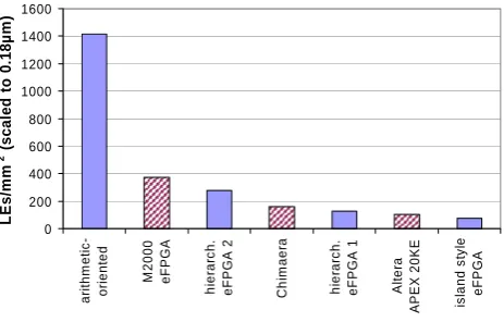
Fig. 14 illustrates the LE-density (number of logic elements
per mm
2) for different (e)FPGA-architectures. It compares
commercial standard FPGAs like the Altera APEX 20K
(Website Altera) or the M2000 FlexEOS-eFPGA (Website
M2000) as well as an exemplary research project, the
Fig. 10. Local and broadcast-interconnect.
Applying the design flow mentioned above, several macros with different parameter settings have been designed in a 180 nm-technology. Two exemplary macros featuring different cluster sizes, different number of LEs per macro and different number and segmentation of routing tracks are depicted in Fig. 8.
For the local CB (CB0 in Fig. 6) a detailed analysis of flexibility requirements has been conducted using a variety of exemplary basic operations. Fig. 9 shows the area fraction of the LEs proportional to the complete macro for different levels of connection box flexibility. The flexibility of the complete architecture is determined by the number of pos-sible connections within a CB. At first, the interconnect of the local CB has been designed for simple arithmetic dat-apaths (e.g. gated full addition, carry-ripple addition etc.). This means that only those connections are realised which are required for ADD/MULT operations. Such a restricted CB would mean that other types of operations cannot be per-formed with this CB configuration. In the next steps, the interconnect structure has been enhanced in a way that mul-tiplexer functionality and randomised logic can be imple-mented (step 2, 3 and 4).
In the following step, more complex arithmetic datapaths have been included (e.g. carry-save arithmetic, CSA). The reference point in this depiction corresponds to the full flex-ible solution (rightmost bars). Above the diagram, the ac-cording layouts of the CB, which are created automatically, are shown. The area fraction of the LEs is directly influenced by the routing parameters described above. Macro 1 includes more global routing tracks. Therefore, this solution features a higher flexibility than macro 2 which has got a more re-stricted routing architecture. The area of the LE and the local CB is the same for both macros.
For this first architecture template, the routing architec-ture is still the dominating factor in terms of area, timing and power consumption. Using the design methodology (see Sect. 4.1) established with the reference architecture, an eFPGA-architecture tailored for an arithmetic-oriented appli-cation domain has been developed.
multipliers. The LEs are connected with a directional
near-est-neighbour interconnect. Rather than providing random
connections to all surrounding neighbours, this structure
reflects the typical nature of arithmetic-oriented datapaths
featuring a preferred data flow direction. In this architecture,
a typical data flow from top to bottom and right to left is
assumed. Diagonal connections are provided in both left-
and right-downwards direction to allow an efficient
imple-mentation of both right- and left-shift-operations. For
effi-cient mapping of datapaths with arbitrary wordlengths,
local connections are also provided across cluster borders.
Signals from the global interconnect, typically representing
operands in datapaths, are distributed along the LEs inside
a cluster as so-called broadcast lines. This is in contrast to
the highly flexible (and large) connection boxes in standard
FPGAs that allow each LE to access global routing
resources. Fig. 10 illustrates this data flow oriented
inter-connect.
Fig. 10
Local and broadcast-interconnect
The logic element used in the arithmetic-oriented eFPGA is
depicted in Fig. 11. The core logic inside the dashed line
consists of two lookup-tables with two inputs each,
dedicated sum- and carry-logic and two latches.
Fig. 11
Arithmetic-oriented
LE
One LUT-2 can be configured as partial-product gate using
the global inputs to enable a direct mapping of
array-multi-plier-based structures to the eFPGA. In addition, the two
lookup-tables can be combined to a single LUT with three
inputs (LUT-3). Dedicated multiplexers allow to connect
the outputs of an LE to the broadcast-lines. The use of two
latches per LE enables efficient pipelining of array-based
datapaths. Rather than using complete registers, small
transmission-gate-based latches reduce the implementation
costs.
The regularity and the typical wordlengths of arithmetic
datapaths allow the shared use of configuration information,
as for example presented in (Ye et al.). In this case, several
logic elements inside a cluster use the same configuration
bits. As the SRAMs storing the configuration typically
amount for about half the area of a logic element,
significant area-reductions can be achieved by choosing the
appropriate granularity for the eFPGA-architecture. The
same concept is applied to the global interconnect lines,
thus reducing the overhead of the costly interconnect
architecture. The overall architecture is shown in Fig. 12.
LE LE LE LE
LE LE LE LE
LE LE LE LE
LE LE LE LE
CB RS
SRAM SRAM SRAM SRAM
LE LE LE LE
LE LE LE LE
LE LE LE LE
LE LE LE LE
CB RS
SRAM SRAM SRAM SRAM
LE LE LE LE
LE LE LE LE
LE LE LE LE
LE LE LE LE
CB RS
SRAM SRAM SRAM SRAM
LE LE LE LE
LE LE LE LE
LE LE LE LE
LE LE LE LE
CB RS
SRAM SRAM SRAM SRAM
Fig. 12
Arithmetic-oriented architecture template
An according eFPGA-macro was designed in a
130nm-technology using a cluster size of 4x4 and a configuration
granularity of four. The global interconnect provides only
16 tracks, as the communication in arithmetic-oriented
datapaths is mainly based on local connections as shown
before. A layout of four complete clusters with
configu-ration blocks, CBs and RSs is shown in Fig. 13.
RS
4x4
LEs
CB
CB
SRAM
RS
4x4
LEs
CB
CB
SRAM
Fig. 13
Layout of arithmetic-oriented eFPGA
As can be seen from the layout, the area of the macro is
dominated by the logic elements, while the area required by
the global interconnect could be reduced significantly. The
area fraction of the LE for the arithmetic-oriented eFPGA is
40%, compared to less than 10% in typical standard FPGAs.
Fig. 14 illustrates the LE-density (number of logic elements
per mm
2) for different (e)FPGA-architectures. It compares
commercial standard FPGAs like the Altera APEX 20K
(Website Altera) or the M2000 FlexEOS-eFPGA (Website
M2000) as well as an exemplary research project, the
Fig. 11. Arithmetic-oriented LE.
4.3 Arithmetic-oriented eFPGA-architecture
The requirements of arithmetic-oriented datapaths have been addressed by the eFPGA architecture described in the follow-ing. The architecture uses arithmetic-oriented LEs that are connected as two-dimensional clusters, reflecting the typical orientation of processing elements in filters and multipliers. The LEs are connected with a directional nearest-neighbour interconnect. Rather than providing random connections to all surrounding neighbours, this structure reflects the typical nature of arithmetic-oriented datapaths featuring a preferred data flow direction. In this architecture, a typical data flow from top to bottom and right to left is assumed. Diagonal connections are provided in both left- and right-downwards direction to allow an efficient implementation of both right-and left-shift-operations. For efficient mapping of datapaths with arbitrary wordlengths, local connections are also pro-vided across cluster borders. Signals from the global in-terconnect, typically representing operands in datapaths, are distributed along the LEs inside a cluster as so-called broad-cast lines. This is in contrast to the highly flexible (and large) connection boxes in standard FPGAs that allow each LE to access global routing resources. Fig. 10 illustrates this data flow oriented interconnect.
The logic element used in the arithmetic-oriented eFPGA is depicted in Fig. 11. The core logic inside the dashed line consists of two lookup-tables with two inputs each, dedicated sum- and carry-logic and two latches.
One LUT-2 can be configured as partial-product gate us-ing the global inputs to enable a direct mappus-ing of array-multiplier-based structures to the eFPGA. In addition, the two lookup-tables can be combined to a single LUT with three inputs (LUT-3). Dedicated multiplexers allow to con-nect the outputs of an LE to the broadcast-lines. The use of two latches per LE enables efficient pipelining of array-based datapaths. Rather than using complete registers, small transmission-gate-based latches reduce the implemen-tation costs.