FABRICATION AND CHARACTERIZATION OF A NEW
MEMS CAPACITIVE MICROPHONE USING
PERFORATED DIAPHRAGM
B. Azizollah Ganji*
Department of Electrical Engineering, Babol University of Technology P.O. Box 484, Babol, Iran
B. Yeop Majlis
Institute of Microengineering and Nanoelectronics (IMEN), University Kebangsaan Malaysia P.O. Box 43600, Bangi, Selangor, Malaysia
*Corresponding Author
(Received: June 10, 2008 – Accepted in Revised Form: December 11, 2008)
Abstract In this paper, a novel single-chip MEMS capacitive microphone is presented. The
novelties of this method relies on the moveable aluminum (Al) diaphragm positioned over the backplate electrode, where the diaphragm includes a plurality of holes to allow the air in the gap between the electrode and diaphragm to escape and thus reduce acoustical damping in the microphone. Spin-on-glass (SOG) was used as a sacrificial and isolating layer. Back plate is mono crystalline silicon wafer, which is much stiffer. This work will focus onthe design, fabrication and characterization of the microphone. The structure has a diaphragm thickness of 3 μm, with 0.5 x 0.5 mm2 size and an air gap of 1.0 μm. The results show that, the pull-in voltage is 105 V, the initial stress
of evaporated aluminum diaphragm is around 1500 Mpa and the zero bias capacitance of microphone is 2.12 pF. Compared with the previous works, this microphone has several advantages: The holes have been made on the diaphragm, therefore there is no need for KOH etching to make the back chamber, in this way the chip size of each microphone is reduced. The fabrication process uses minimum number of layers and reduces the fabrication cost.
Keywords MEMS Microphone, Perforated Diaphragm, SOG Sacrificial Layer, Silicon Backplate
ﻜﭼ
ﻴ
ﻩﺪ
ﻧﺯﺎﺧﻥﻮﻓﻭﺮﮑﻴﻣﮏﻳﻪﻟﺎﻘﻣﻦﻳﺍﺭﺩ ﻲﮊﻮﻟﻮﻨﮑﺗﺯﺍﻩﺩﺎﻔﺘﺳﺍﺎﺑﺪﻳﺪﺟ ﻱ ﻦﻴﺷﺎﻣ ﯽﻧﻭﺮﮑﻴﻣﯼﺭﺎﮐ ﻪﺿﺮﻋ ﯽﻣ ﺩﻮﺷ . ﻦﻳﺍ ﯼﺭﻭﺁﻮﻧ ﺪﺘﻣ
ﻪﻋﻮﻤﺠﻣ ﻞﻣﺎﺷ ﻪﮐ ﺖﺳﺍ ﺖﮐﺮﺣ ﻞﺑﺎﻗ ﻢﮔﺍﺮﻓﺎﻳﺩ ﮏﻳ ﻦﺘﺧﺎﺳ ﺭﺩ ﻩﺮﻔﺣ ﺯﺍ ﯼﺍ
ﺎﻫ ﺶﻫﺎﮐ ﺖﻬﺟ ﺍﻮﻫﮓﻨﻴﭙﻣﺩ ﺭﺩ ﺔﻠﺻﺎﻓ ﺍﻮﻫ ﻳ ﻭﻢﮔﺍﺮﻓﺎﻳﺩ ﻦﻴﺑﯽ ﺍ ﺩﻭﺮﺘﮑﻟ ﺖﺑﺎﺛﻪﺤﻔﺻ ﯽﻣ ﺩﻮﺷ . ﺩﺎﻣﻦﻴﻨﭽﻤﻫ ﺓ SOG ﻪﺑ ﺕﺭﻮﺻ ﻳﻻ ﺔ ﻭﻥﻮﻓﺪﻣ ﺑﺖﺑﺎﺛ ﻪﺤﻔﺻﻭﻢﮔﺍﺮﻓﺎﻳﺩ ﻦﻴﺑ ﻩﺪﻨﻨﮐ ﻪﻟﻭﺰﻳﺍ ﻪ ﺭﺎﮐ ﺭ ﺖﺳﺍ ﻪﺘﻓ . ﺤﻔﺻ ﺔ ﺮﻔﻳﻭ ﺯﺍﯽﻧﺯﺎﺧ ﻥﻮﻓﻭﺮﮑﻴﻣ ﺖﺑﺎﺛ
ﯽﻟﺎﺘﺴﻳﺮﮐﮏﺗﯽﻧﺎﮑﻴﻠﻴﺳ ﺖﺳﺍ
ﺖﺳﺍﺮﻳﺬﭘﺎﻧﺶﻤﺧﻭﺖﺨﺳﺭﺎﻴﺴﺑﻪﮐ .
ﻭﺭﺮﺑﺭﺎﮐﻦﻳﺍ ﻱ
ﺣﺍﺮﻃ ﻲ ، ﺖﺴﺗﻭﺖﺧﺎﺳ
ﺍﺰﮐﺮﻤﺘﻣﻥﻮﻓﻭﺮﮑﻴﻣ ﺖﺳ
. ﻟﺁ ﻢﮔﺍﺮﻓﺎﻳﺩ ﮏﻳﯼﺍﺭﺍﺩ ﻥﻮﻓﻭﺮﮑﻴﻣﻥﺎﻤﺘﺧﺎﺳ ﻮ
ﻴﻨﻴﻣ ﻮ ﺖﻣﺎﺨﺿﻪﺑﯽﻣ ۳ ﺮﺘﻣﻭﺮﮑﻴﻣ ﺩﺎﻌﺑﺍ ﺎﺑ ۰ / ۵ x ۰ / ۵ ﻊﺑﺮﻣﺮﺘﻣﯽﻠﻴﻣ ﻠﺻﺎﻓﮏﻳﻭ
ﺔ ﺍﻮﻫ ﻳ ﺯﺍﺪﻧﺍﻪﺑﯽ ﺓ ۱ ﺮﺘﻣﻭﺮﮑﻴﻣ ﺖﺳﺍ . ﻣﻥﺎﺸﻧﻪﺠﻴﺘﻧ ﻲ
ﮊﺎﺘﻟﻭﻪﮐﺪﻫﺩ
Pull-in ﻥﺁ ۱۰۵ ﺖﻟﻭ ﻴﻟﻭﺍ ﺱﺮﺘﺳﺍ ﺔ ﻟﺁﻢﮔﺍﺮﻓﺎﻳﺩ ﻮ ﻴﻨﻴﻣ ﻮ ﯽﻣ ۱۵۰۰ ﻝﺎﮕﺳﺎﭘﺎﮕﻣ ﺯﺍﺪﻧﺍ ﻭ ﺓ ﺭﺩﻥﺯﺎﺧ ﺮﻔﺻ ﺱﺎﻳﺎﺑ ۲ / ۲ ﺩﺭﺎﻓﻮﮑﻴﭘ ﺖﺳﺍ . ﺎﺑﻪﺴﻳﺎﻘﻣﺭﺩ ﺩﺭﺍﺩﺖﻳﺰﻣﻦﻳﺪﻨﭼﻥﻮﻓﻭﺮﮑﻴﻣﻦﻳﺍﻩﺪﺷﻡﺎﺠﻧﺍﯼﺎﻫﺭﺎﮐ
: ﻩﺮﻔﺣ ﺎﻫ ﻩﺪﺷﻪﺘﺧﺎﺳﻢﮔﺍﺮﻓﺎﻳﺩﯼﻭﺭﺮﺑ ﺪﻧﺍ
ﺵﻭﺭﺯﺍﻩﺩﺎﻔﺘﺳﺍﺎﺑﺍﻮﻫﮓﻨﻴﭙﻣﺩﺶﻫﺎﮐﺖﻬﺟﻥﺯﺎﺧﺖﺑﺎﺛﻪﺤﻔﺻﺭﺩﯽﺒﻘﻋﺮﺒﻤﭼﺖﺧﺎﺳﻪﺑﺯﺎﻴﻧﻪﮐ
KOH
ﺭﺍﺪﻧ ؛ﺩ
ﺯﺍﺪﻧﺍﻪﺠﻴﺘﻧﺭﺩ ﺓ
ﯽﻣﺶﻫﺎﮐﻥﻮﻓﻭﺮﮑﻴﻣ ﺑﺎﻳ
ﺪ . ﻣﻦﻳﺍﺖﺧﺎﺳﯼﺍﺮﺑ ﻴ
ﻪﻳﻻﻞﻗﺍﺪﺣﺯﺍﻥﻮﻓﻭﺮﮑ ﺎﻫ
ﻱ ﻩﺪﺷﻩﺩﺎﻔﺘﺳﺍﺯﺎﻴﻧﺩﺭﻮﻣ
ﻪﮐﺖﺳﺍ ﺚﻋﺎﺑ ﺖﻤﻴﻗﺶﻫﺎﮐ ﺪﺷﺪﻫﺍﻮﺧﻪﻋﻮﻤﺠﻣ
.
1. INTRODUCTION
MEMS Microphone is a transducer that converts acoustic energy into electrical energy. In accordance
with the need for very small devices, the microphones are required to be quite small with high performance.
voice communications devices, hearing aids, surveillance and military aims, ultrasonic and acoustic distinction under water, noise and vibration control [1]. The micromachining technology has been used to design and fabricate various silicon microphones. Among them, the capacitive microphone is the highest number produced, for its high sensitivity, high signal to noise ratio, and durability [2].
Typically, a cavity is etched into a silicon substrate by slope (54.74˚) etching profiles using KOH etching, in order to form a thin diaphragm or perforated backplate [3-8]. Forming a cavity or back chamber from the wafer backside by KOH etching is slow and boring in that several hundred microns of substrate may need to be etched to make the chamber. Moreover, KOH etching process is not more compatible with CMOS process. Additionally, since the back plate needs acoustic holes which have to be etched from the back side in the deep back volume cavity, a nonstandard photolithographic process had to be used which needs electrochemical deposition of the photoresist and an aluminum seed layer. Most surface and bulk micromachined capacitive microphones uses fully clamped diaphragm with perforated backplate [9,10]. Process for their fabrication are typically long, cumbersome, expensive, and not compatible with high volume process. Furthermore, they are not small in size. Many conventional MEMS capacitive microphones are fabricated in high temperature [11,12], where the structure is damaged.
It is the objective of this research to overcome the existing disadvantages of the prior fabrication of a novel MEMS capacitive microphone, which utilizes perforated aluminum diaphragm, monocrystalline silicon wafer as a backplate, and spin-on-glass (SOG) as sacrificial and isolating layer between backplate and diaphragm, at least achieving a small size, low cost and easy to fabricate microphone structure.
2. MICROPHONE DESIGN
The structure of the new microphone is shown in Figure 1. It consists of a rigid monocrystalline backplate, an aluminum diaphragm with holes, and
the backplate electrode is a n+-doped layer. An
acoustic wave striking the diaphragm, causes its flexural vibration and changes the average distance from the back plate. The change in distance will produce a change in capacitance, giving rise to a time varying voltage on the electrodes. The structure parameter of the microphone includes the dimension of the diaphragm, the size and density of the holes in the diaphragm, the dimension of the backplate and the height of the air gap. In our design, the thickness of the 0.5 mm x 0.5 mm membrane is 3 µm, the density of the 20 µm x 20 µm acoustic holes is 144/mm2, the height of the air
gap is about 1 µm.
3. MICROPHONE FABRICATION
In this section we describe a fabrication process developed in the Institute of Microengineering and Nanoelectronics (IMEN) laboratories. The process uses five masks and starts with a single side polished p-type (100) silicon wafer as a substrate. Figure 2 illustrates fabrication-process flow of the microphone structure.
3.1. n
+Phosphorus Diffusion
A 0.2 µm thick wet oxide is grown on silicon wafer. This oxide layer is patterned and etched in the buffered HF serving as a mask for the phosphorus diffusion. Then, a n+ phosphorus diffusion was introducedinto the p-type (100) silicon wafer as a bakeplate electrode at 1000˚C, for 30 minutes in 70% nitrogen and 30% oxygen gas ambient. A constant source diffusion process was used to obtain the n+
-silicon layer with a depth of 0.4 µm and surface concentration as high as 1020 atoms/cm3 (Figure 2a).
3.2. Sacrificial and Isolating Layer
Deposition
Silicon dioxide is usually a chosensacrificial material and insulating layer, since it can be easily deposited and removed using PAD etch solution. Moreover, PAD etch has a high selectivity to silicon dioxide compared to silicon and Al, thus it completely removes sacrificial oxide without incurring significant damage silicon wafer and Al. Spin-on glass (SOG) is an alternative method to deposit planarized oxide. As its name indicates, SOG is usally spun using spin coater. In this study siloxane type Accuglass 314 SOG from Honeywell Inc. is chosen due to its high crack resistance, excellent gap fill, good adhesion between layers, high thermal stability, and good planarization property of cured film. The layer then gradually hot plated at 200˚C and maintained at the peak temperature for a few minutes and gradually cooled down to avoid internal stress build up. Baking temperature needs to be high enough to efficiently evaporate solvent from the SOG. On the other hand, baking temperature beyond 200˚C would cause the SOG to lose its thickness. Temperature of 200˚C is therefore chosen as optimal baking temperature to take 1 μm thick SOG as a sacrificial and insulating layer between diaphragm and back plate. The isolating layer is then patterned and etched in PAD etch solution for 3.5 minutes to define the contact area on the back plate (Figure 2b).
3.3. Diaphragm Making
A 3 µm thickaluminum was deposited on SOG layer by metal evaporator as diaphragm. The Al layer is then patterned using photoresist mask to define the geometry of the perforated diaphragm, and contact pad, and then etched by Al etchant (Figure 2c). Etchant for aluminium is 16:4:1 of phosphoric acid (H3PO4), DI water, and nitric acid
(HNO3). The etch rate of Al in Al etchant is 930
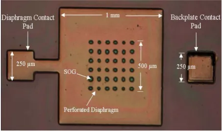
Å/minute. First the structure was immersed in Al etchant for 35 minutes to etch the Al for making diaphragm structure with holes (Figure 2d). A microscope was used to determine whether the Al had been removed and how successfully the Al was etched. Below, Figure 3 is an optical microscope top view of the surface of the microphone. It can be seen that Al was removed from holes. The green color is SOG sacrificial layer.
(a)
(b)
(c)
(d)
(e)
Figure 2. Microphone fabrication process, (a) n+ diffusion as a
backplate electrode, (b) SiO2 deposition as a sacrificial and
3.4. Sacrificial Silicon Oxide Etching by
PAD Etchant
Figure 4 shows the variation ofAl thickness with etch time in PAD etchant. According to Figure 4, the approximate etch rate of Al in PAD etch in room temperature is 30.6 Å/minute. Figure 5 shows the variation of SOG thickness with etch time in PAD etchant. According to Figure 5 the approximate etch rate of SOG in PAD etch in room temperature is 4300 Å/minute. Therefore PAD etchant shows a high selectivity against Al. The thickness of Al and SOG were measured using surface profiler (Figure 2e). For sacrificial layer etching, the structure was immersed in a PAD etch bath to remove the sacrificial layer of oxide. The wafers were placed directly onto the bottom of the bath’s container and there was some agitation throughout the etching process. The wafers were taken out, and rinsed to remove the PAD etchant. The final step was to remove the photoresist by immersing the wafer into an acetone bath, and then the wafer is dried using hot plate at 60˚C for 90 secs.
After the completion of above process on the wafers, the last step was to determine if the fabrication process had been successful. It is important to observe the silicon membrane and check to ensure that the oxide layer was uniformly removed. All testing was performed by using a Scanning Electron Microscope (SEM) and optical microscope to capture images of the membrane surface and images of the cross-section. The calculated sacrificial layer etch time is about 70 minutes. Figure 6 shows the surface of the microphone with photoresist layer after 75 minutes wet etching in PAD etch solution under optical microscope.
Our experience shows that, by increasing the etching time, the diaphragm surface color is changed during the sacrificial layer etching in PAD etch solution. It means that, the sacrificial layer goes to be removed under Al diaphragm. As shown in Figure 6, a problem was that, the PAD etch solution after 35 minutes was influenced between photoresist layer and Al diaphragm, then broken and removed photoresist from the surface of membrane. It is due to poor adhesion between resist and Al diaphragm, but it is not important during the sacrificial etching using PAD etch solution, because of PAD etchant has a high selectivity against Al. Figure 7 shows the released
Figure 3. Optical microscopy top view of the microphone.
Figure 4. Variation of Al thickness with etch time.
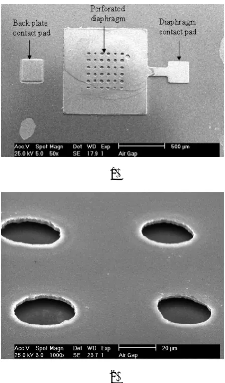
membrane structure after 75 minutes etching in PAD etchant. The final product shows the sacrificial layer between Al diaphragm and silicon backplate has been completely removed. Figure 8a shows the surface of the fabricated microphone in MEMS laboratory of IMEN and Figure 8b shows the close up view of the Al diaphragm surface with acoustic holes using SEM after 75 minutes etching in PAD etchant. It was obvious that the Al sidewalls were not smooth, because of mask problem, but all of the holes have been etched.
4. RESULTS AND DISCUSSION
4.1. Pull-in Voltage
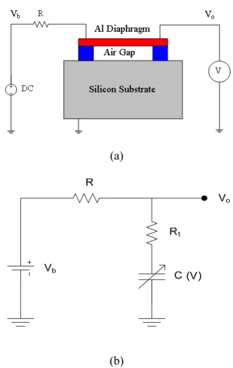
Figure 9 shows the structure and equivalent test circuit for VPI measurement[13]. The basic principle involves the well-known pull-in voltage. When a voltage Vb is applied
across the air gap, the electrostatic force causes the diaphragm to deflect toward the substrate. An increase of the deflection of the membrane results in a decrease of the gap spacing and thus in an increase of the electrostatic force. If Vb exceeds the
so-called pull-in voltage VPI, the deflection does
not reach an equilibrium position and will
Figure 6. Optical microscopy top view of device with photoresist
after 75 minutes in PAD etch solution.
Figure 7. SEM images of released membrane structure.
(a)
(b)
Figure 8. (a) The surface of the fabricated microphone and (b)
continue to increase until physical contact is made with the bottom electrode. VP I value was
measured by the use of the test circuit shown in Figure 9b. Vo maintains the same value as Vb,
(Vo=Vb), and increased with Vb at the beginning.
When Vb reaches VPI, Vo suddenly decreases,
(Vo=Rt/(Rt+R)*Vb), because of the discharge of
the conductive membrane (the upper electrode) due to the physical contact of the membrane and the silicon substrate (the lower electrode). As shown in Figure 10, the pull-in voltage of microphone is 105 V.
4.2. Internal Stress of Diaphragm
Since the pull-in voltage, VPI, on the stiffness of themembrane which is a function of the internal stress, σ, the internal stress of the membrane can be calculated using equation below [14]:
⎥ ⎥ ⎥
⎦ ⎤
⎢ ⎢ ⎢
⎣ ⎡
⎟ ⎟ ⎠ ⎞ ⎜ ⎜ ⎝ ⎛ ν + ⎟ ⎟ ⎠ ⎞ ⎜ ⎜ ⎝ ⎛ σ ε
=
3
3 0 d 4 aˆ
^ E t ) ( 2 C 3
0 d 2 aˆ
t 1 C 0 5
2 0 d 6 PI
V (1)
where d0 is air gap thickness, t, diaphragm
thickness, Ê, Young’s modulus, v, Poisson’s ratio, â, the half of the diaphragm side length and. The quantities, C1 and C2 are numerical parameters.
When the pull-in voltage and the geometry are known. We found the collapse voltage of 105 V for a square membrane of 0.5 x 0.5 mm2, thickness of
3 µm and air gap of 1 µm resulting in an internal stress of 1500 MPa for the aluminum membrane.
4.3. The Capacitance of the Microphone
The capacitance of the microphone was measured using LCR meter. Figure 11 shows the capacitance versus bias voltage. The zero bias capacitance, corresponding to an air gap of about 1 μm was 2.12 pF. The capacitance increased with increasing bias voltage due to the decrease in the air gap thickness as the Al membrane is electrostatically pulled towards the back plate. The bias voltage was increased from zero until the pull-in of the bending membrane was observed.
4.4. Diaphragm Deflection
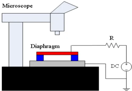
The measurement of central deflection of diaphragm, d, versus bias voltage is performed with an optical measurement set-up using a z-stage calibrated optical microscope.(a)
(b)
Figure 9. Schematic diagram of the basic test structure and circuit for VPI measurement, (a) test structure and (b) equivalent
circuit.
0 20 40 60 80 100 120
0 20 40 60 80 100 120
Vb (V)
Vo
(
V
)
In Figure 12, the principal set-up is drawn. The silicon substrate with a flat diaphragm is connected to a DC voltage. A differential voltage applied to the diaphragm causes it to deflect. By successively focusing the microscope at an increasing voltage value, the center deflection of the diaphragm can be measured. Figure 13 shows the diaphragm deformation versus voltage under bias conditions from 0 V to 120 V. The Al diaphragm thickness is 3 µm and its side length is 0.5 mm. The deflection as a function of voltage increases slightly until a drastic change occurs indicating the collapse of the membrane into the backplate. This curve can be naturally divided into four regions. In the first linear region for small bias voltages, the
electrostatic forces are insignificant compared with the pressure load. For intermediate voltage, the electrostatic forces have a notable influence. In the region close to structural collapse, the influence becomes significant enough for the system to becomes unstable at the pull-in voltage, where the diaphragm of the microphone is displaced about one-third of the original gap. Above the critical bias voltage, the structure collapses. Considering the relationship between deflection and the bias voltage, the working voltage is often restricted to the linear region. In our simulations, the upper limit of the linear range is about 60 % of the pull in voltage. The experimental result shows that the pull-in occurs around 105 volts and this is in agreement with the simulation value.
4.5. Sensitivity and Frequency Response of
the Microphone
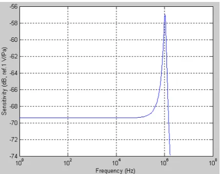
The magnitude (sensitivity) and the frequency phase response were simulated using experimental parameters of the microphone (residual stress and pull-in voltage). Figure 14 shows the sensitivity of the microphone as a function of frequency for 1 Hz to 100 kHz range. The thickness of Al diaphragm and air gap of the microphone, measured by surface profiler, are 3μm and 1 μm, respectively. As can be seen the maximum sensitivity of the microphone is 0.2 mV/Pa with bias of 105 V. Figure 14, showes the frequency response is flat in hearing range (1Hz to 20 kHz) and sensitivity exhibits a gradual increase at higher frequencies (out of hearing range).
5. CONCLUSION
In this paper, a novel single-chip capacitive microphone was successfully designed and fabricated using MEMS process. The microphones’ chip size is reduced, the complex and expensive fabrication process was avoided by making holes in diaphragm. The fabrication process uses minimal number of layers and masks to reduce the fabrication cost. Back plate is a mono crystalline silicon wafer, which is much stiffer. The temperature used for fabrication is less than 200˚C, thus reducing temperature induced the damages. The diaphragm size is about 0.5 x 0.5 mm2 which is
smaller than conventional MEMS capacitive
0 20 40 60 80 100 120
2.1 2.2 2.3 2.4 2.5 2.6 2.7 2.8 2.9 3
C
a
pa
c
it
a
n
c
e (
p
F
)
Bias voltage (V)
Figure 11. Microphone capacitance vs. bias voltage.
microphone. SOG sacrificial layer is easy to deposit by spin coater and also easy to release by PAD etch solution. Al diaphragm is electrically conductive, thus no extra electrode is needed. The results show that the maximum sensitivity of microphone is 0.2 mV/Pa, and the frequency response is flat in hearing range.
6. REFERENCES
1. Ma, T. and Man, T.Y., “Design and Fabrication of an
Integrated Programmable Floating-Gate Microphone,
IEEE, (2002), 288-291.
2. Jing, C., Liu, L., Zhijian, L., Tan, Z., Xu, Y. and Ma, J., “On the Single-Chip Condenser Miniature Microphone using DRIE and Back Side Etching Techniques”,
Sensors and Actuators A, Vol. 103, (2003), 42-47.
3. Scheeper, P.R., Olthuis, W. and Bergveld, P., “A Silicon Condenser Microphone with a Silicon Nitride Diaphragm and Backplate”, J. Micromec. Microeng,
Vol. 2, (1992), 187-189.
4. Kronast, W., Muller, B., Siedel, W. and Stoffel, A., “Single-Chip Condenser Microphone using Porous Silicon as Sacrificial Layer for the Air Gap”, Sensors
and Actuators A, Vol. 87, (2001), 188-193.
5. Pedersen, M., Olthuis, W. and Bergveld, P., “A Silicon Condenser Microphone with Polyimide Diaphragm and Back Plate”, Sensors and Actuators A, Vol. 63, (1997),
97-104.
6. Bergqvist, J. and Gobet, J., “Capacitive Microphone with a Surface Micromachined Backplate using Electroplating Technology”, Journal of Microelectromechanical
Systems, Vol. 3, No. 2, (1994), 69-75.
7. Torkkeli, A., Rusanen, O., Torkkeli, Al., Rusanen, O., Saarilahti, J., Seppa, H., Sipola, H. and Hietanen. J., “Capacitive Microphone with Low-Stress Polysilicon Membrane and High-Stress Polysilicon Backplate”,
Sensors and Actuators, Vol. 85, (2000), 116-123.
8. Kabir, A.E., Bashir, Bernstein, J., Santis, J.D., Mathews, R., O’Boyle, J.O. and Bracken, C., “High Sensitivity Acoustic Transducers with thin P+ Membrane and Gold
Back-Plate”, Sensors and Actuators A, Vol. 78, (1999),
138-142.
9. Ning, J., Liu, Z., Liu, H. and Ge, Y., “A Silicon Capacitive Microphone Based on Oxidized Porous Silicon Sacrificial Technology”, IEEE, (2004), 1872-1875.
10. Ning, Y.B., Mitchell, A.W. and Tait, R.N., “Fabrication of a Silicon Micromachined Capacitive Microphone using a Dry-Etch Process”, Sensors and Actuators A, Vol. 53, (1996), 237-242.
11. Hsu, P.C., Mastrangelo, C.H. and Wise, K.D., “A High Density Polysilicon Diaphragm Condenser Microphone”,
Conference Record IEEE 11th International Workshop
on Microelectro Mechanical Systems (MEMS), (1988),
580-585.
12. Chowdhury, S., Jullien, G.A., Ahmadi, M.A. and Miller, W.C., “MEMS Acousto-Magnetic Components for use in a Hearing Instrument”, Presented at SPIE’s Symposium on Design, Test, Integration, and Packaging of MEMS/MOEMS, Paris, Frence, (2000).
13. Zou, Q., Li, Z., and Liu, L., “New Methods for Measuring Mechanical Properties of thin Films in Micromachining: Beam Pull-In Voltage (VPI) Method and Long Beam
Deflection (LBD) Method”, Sensors and Actuators A, Vol. 48, (1996), 137-143.
14. Majlis, B.Y. and Ganji, B.A., “Pull-In Voltage and Diaphragm Deflection Analysis of MEMS Capacitive M i c r o ph o ne ” , I n t e r n a t i o n a l C o n f e r e n c e o n Instrumentation, Communication and Information
Technology (ICICI), (2005), 772-779.
0 20 40 60 80 100 120
0 0.1 0.2 0.3 0.4 0.5 0.6 0.7 0.8 0.9 1
C
ent
ra
l
def
le
c
ti
on of
di
aphr
agm
(
u
m
)
Bias voltage (V)
Figure 13. The central deflection vs. bias voltage.