*Corresponding author: Rodrigues, AV ISSN: 0976-3031
Research Article
GALLIUM OXIDE: A PERSPECTIVE OF FEATURES IN PHOTOLUMINESCENCE
AND GAS SENSOR APPLICATIONS
Rodrigues, AV* and Sabino, NL
Department of Physical Chemistry, Institute of Chemistry, UNESP University,
Araraquara/SP- Brazil
DOI: http://dx.doi.org/10.24327/ijrsr.2019.1011.4176
ARTICLE INFO ABSTRACT
In the last years, it was increased the object of studies regarding the semiconductor metallic oxide nanostructures, whose applications in photoluminescence and sensor are originated from their optoelectronic and electronic properties. The gallium oxide is an ultra wide bandgap material (4.9 eV) which presents UV photodetection properties and intense blue photoluminescence. Chemical processes control and environmental monitoring are the main factors which directly influence the
morphology, crystallite size and porosity of the Ga2O3. Several techniques are able to synthesize
these materials, preferable one-dimensional nanostructures because their large surface areas enable the improvement of the photoluminescence features. The driving force for the very broad and intense photoluminescence emission spectrum in the blue region of the wavelength was the presence
of oxygen vacancies in the β-Ga2O3 nanofibers. Two types of Ga3+ ions, octahedral and tetrahedral
chains, came from the different vibrations of Ga–O bonds. Their suitable electrical properties can also increase the sensor response, sensitivity, and thermal stability to different sorts of gases. Green synthesis, low cost, and versatility of nanostructures growth in single step have attracted much attention of the researchers. In this review, there are showed a great perspective of the gallium oxide properties, the most techniques applied to synthesize the materials, and general applications of this material.
INTRODUCTION
Due to their structural, electrical, piezoeletric and optoelectronic properties, one-dimensional semiconductor nanostructures have received great attention regarding their application, e.g. as light-emitting-diodes and gas sensors. Since the 1960s, it has been focused on syntheses of nanostructured metal oxides with desirable sizes and shapes (Mirzaei and Neri, 2016; Abdullah, Yam, Mohmood et al., 2016; Tian et al., 2012).
The -Ga2O3 structure is the stablest phase of gallium oxide, with good chemical and thermal stabilities, good conductivity and considerable luminescent properties, features that extremely depend on the gallium and oxygen vacancies (Abdullah, Yam, Mohmood et al., 2016). The photoluminescence behavior of the Ga2O3 nanocrystals is influenced by thermal treatments, which control the crystallinity and surface structures. And crystallinity, crystallite defects, and surface area have a great impact on the photoluminescence properties (Wang, Widiyastuti, Ogi et al., 2007; Girija, Thirumalairajan, and Mangalaraj, 2014; Liu,
Wang, Cai et al., 2009). The decrease of the average separation of the charged donor and the acceptor vacancy sites originates the increase of the photoluminescence intensity with slight shifting of the emission bands, as well as the decrease of the particle size which affects the Stokes shift band (Wang and Radovanovic, 2011; Víllora et al., 2002). It is well-known that blue photoluminescence behavior of Ga2O3 nanocrystals, for instance, is controlled by the oxygen vacancies through the kinetic annealing in solution (Zhou et al., 2016; Ge and Zheng, 2009), and the oxygen vacancies and oxygen-gallium vacancy pairs are originated by the larger specific areas, thus affecting the emission intensities (Terasako, Kawasaki, and Yagi, 2016; Wang, Tang, Zeng et al., 2018). Herein, broadness, intensity of emission band, and the range of the wavelength enable the Ga2O3 to be applied in optoelectronic devices (Wang and Radovanovic, 2011; Zhou et al., 2016; Ge and Zheng, 2009). Characteristics as speed of response, stability and high sensitivity also make the mentioned material enabled to the gas sensor application. Gas sensors of semiconductor metal oxides generally exhibit thermal stability and high sensitivity to pollutant, toxic and flammable gases (Gao et al., 2013). Due to
Available Online at http://www.recentscientific.com
International Journal of
Recent Scientific
Research
International Journal of Recent Scientific Research
Vol. 10, Issue, 11(B), pp. 35816-35827, November, 2019
Copyright © Rodrigues, AV and Sabino, NL, 2019, this is an open-access article distributed under the terms of the Creative Commons Attribution License, which permits unrestricted use, distribution and reproduction in any medium, provided the original work is properly cited.
DOI: 10.24327/IJRSR
CODEN: IJRSFP (USA)
Article History:
Received 14th August, 2019
Received in revised form 29th
September, 2019
Accepted 05th October, 2019
Published online 28th November, 2019
Key Words:
International Journal of Recent Scientific Research Vol. 10, Issue, 11(B), pp. 35816-35827, November, 2019
large nanostructure surface to volume ratio that facilitates the interaction of the larger surface with the surrounding environment, superior gas sensor properties are promoted by one-dimensional (1D) semiconductor nanostructured materials (Calestani et al., 2017). So far, interaction mechanisms between the sensor surface and the gas have been deeply studied, realizing that gas sensors with low cost production, fast response, and excellent stability are desired (Wang, Wang, Sun et al., 2016). However, the sensor properties of 1D Ga2O3 materials are not further studied, e.g. the conductivity mechanism of Ga2O3 via measurements at high in situ temperatures, and the influence of both density and load mobility into the electronic conductivity of the sensor output (Hoefer, Frank, and Fleischer, 2001).
In this review, there will be exposed some methods of synthesis and characterization, as well as structural, electronic and optical properties of low-dimensional Ga2O3 nanostructures that are attracting attention for photoluminescence and gas sensor applications.
Gallium Oxide Properties
Ga2O3 has attracted much attention as an emerging material suitable for power devices, once it demonstrated the successful growth of its crystals. The Ga2O3 crystal polymorphs are synthesized from gallia gel, GaOOH. The five isomorphic structures, α-, β-, γ-, δ-, and ɛ-Ga2O3 are well reproduced. The β-Ga2O3 is the stablest phase that can be converted from other phases through annealing temperature. The α-Ga2O3 is the second stablest phase, which can be obtained after 12 h of GaOOH annealing at approximately 500 °C. The metastable low-temperature phase, γ-Ga2O3, is originated when the temperature of GaOOH annealing is between 400 and 500 ºC. A mixture of GaOOH and α-Ga2O3 phases can also occur at 400 °C, a pure phase of α-Ga2O3 is possible at 500 °C, a mixture of α-Ga2O3 and β-Ga2O3 is formed at 600 °C, and a pure β-Ga2O3 is obtained at 700 °C (Akazawa, 2016). The metastable phase of -Ga2O3 can be obtained from α-Ga2O3 at 500 °C, as well as from -Ga2O3 under a range of annealing temperature at approximately 550 °C (Ge and Zheng, 2009). And the -Ga2O3 can be prepared between 200 and 250 °C by heating the residual of evaporated Ga(NO3)3 solution (Li, Wei, and Behrens, 2012).
The Ga2O3 belongs to the family of conducting transparent semiconducting oxides, and it has extensive applicability. Prepared under specific conditions, the polymorphs , , , , and phases are different regarding their space group and coordination number of Ga ions (Delgado and Areán, 2005; Stepanov et al., 2016). Several similarities, such as structural and optical properties, are exhibited between Ga2O3 and aluminum oxide (Al2O3), although the alumina is an insulator. The gallium oxide has high melting point between 1800 °C and 1900 °C. Usually, it is an insulator at room temperature with a forbidden energy gap of 4.9 eV, and a semiconductor above 800 °C. Oxygen vacancies increase the n-type semiconductor property when the Ga2O3 is calcined in a reducing atmosphere, which leads the number of gallium oxide applications, such as gas sensor, catalysts, synthesis of solid electrolytes, or in other words, generally fabrications of optoelectronic and sensing devices (Bartic, 2016; Hirano et al., 2015; Yang, Zhao, and Frost, 2009).
Even it is exposed to concentrated acids, e.g. hydrofluoric acid, the -Ga2O3 is the chemically and thermodynamically stablest phase (Abdullah, Yam, Mohmood et al., 2016; Altuntas et al., 2014). In general, the -Ga2O3 has a gap between 4.4 and 4.9 eV at room temperature, with high crystallinity as the α-Ga2O3 compound. The beta phase can be obtained by baking any other polymorph phase of the Ga2O3 in air at high temperatures, usually from the ones above 700 °C, being possible to reach 950 °C with high crystallinity (Abdullah, Yam, Mohmood et al. 2016; Terasako, Kawasaki, and Yagi, 2016; Delgado and Areán, 2005; Stepanov et al., 2016; Cuong, Park, and Yoon, 2009). As it is depicted in Figure 1, the three-dimensional structure and coordination of -Ga2O3 show its 2/ space group and monoclinic structure, with two distinct gallium sites as six- and four-coordinated, and three oxygen sites as three- and four-coordinated. The nature of the semiconductor as n-type is due to the presence of oxygen vacancies, which act as donor states (Abdullah, Yam, Mohmood et al., 2016; Calestani et al., 2017). Structures, luminescence, and electrical properties of -Ga2O3 nanowires, nanobelts, and nanorods have been attractive for the fabrication of optoelectronic devices due to their high photoresponse for UV light (Zhong et al., 2015). Much attention is also received from the size- and shape-controlled growth of -Ga2O3 nanostructures. The decrease in crystallite size during the nanostructures formation, vapor concentration, relative humidity, film thickness, and other factors improve the device gas-sensing performance (Terasako, Kawasaki, and Yagi, 2016; Pandeeswari and Jeyaprakash, 2014). An example is showed in Figure 1, where the unit cell of three-dimensional structure and the coordination of -Ga2O3 can be visualized with the distinct gallium sites.
Unit cell of three-dimensional structure and coordination of
-Ga2O3
Figure 1 Unit cell of three-dimensional structure and coordination of β-Ga2O3:
2/ space group with distinct gallium sites as four- and six-coordinated (Ga1
and Ga2 coordinated tetrahedrally and octahedrally coordinated with oxygen atoms).
Rodrigues, AV and Sabino, NL., Gallium Oxide: A Perspective of Features In Photoluminescence And Gas Sensor Applications
Collins, Baltanás, and Bonivardi, 2006; Roberts Under high pressure, it is generally likely to obtain the α at about 500 °C (Roberts et al., 2018). It can also be obtained via thermal decomposition of the as-prepared GaOOH at 600 °C (Quan et al., 2010). The literature describes that there is a conservation of initial shape and size of the aggregates during the phase transformation from α-GaOOH to α
its platelet-like shape gradually fades as the temperature of calcination is increased to 350 °C. Some researchers have been identified a mixture of α-GaOOH and α-Ga
pure compound of α-Ga2O3 at 500 °C, a mixture of α and -Ga2O3 at 600 °C, and a pure compound of
700 °C (Akazawa, 2016; Li, Wei, and Behrens, 2012). It is possible to apply the α-Ga2O3 as ultraviolet optoelectronics and power devices due to its energy gap, with a ranging from 3.8 eV (α-In2O3) to 8.8 eV (α-Al2O3) (Roberts et al.
The -Ga2O3 compound was first obtained in 1952 by heating the “δ-Ga2O3” at 550 °C, which is merely a nanocrystalline form of -Ga2O3 and not a distinct polymorph. Nowadays, it is poorly described in scientific research, and sometimes it can be identified as -Ga2O3 (Ge and Zheng, 2009;
2016). It originates the β phase when the thermal annealing reaches temperatures of 700-1000 °C under different atmospheres (Fornari et al., 2017). Its physical property enables the fabrication of electronic devices using the own Ga2O3 material or -Ga2O3 combinations with other materials that have high energy gap values. The
crystallized in the hexagonal () form with space group of
6 (like hexagonal GaN) or orthorhombic (
with 2 space group, depending on the size of the ordered domains and resolution of the used crystallization probe. The orthorhombic domains with small dimensions are able to be detected only by electron diffraction at the nanoscale (Fornari et al., 2017; Pavesi et al., 2018; Oshima et al.
The -Ga2O3 can be prepared between 200 and 250 °C by heating the residual of evaporated Ga(NO
crystallizes like In2O3 in the C-type structure of rare is possible to modify the - to the orthorhombic
system by heating it above 500 °C. The polymorphism of Ga2O3 is very similar to the Al2O3: -, -,
isomorphous with -, -, - (or -), and -Al
However, there is no form of Al2O3 that corresponds to Ga2O3 (Li, Wei, and Behrens, 2012). Promising results were also related to high surface area Ga2O3 for the photocatalysts degradation of air pollutants using UV-C light. This was a soft route of -Ga2O3 synthesis that could be performed through the gas-phase photocatalytic oxidation reactions under UV
stably converting toluene to CO2. The process of toluene conversion and mineralization rate into CO2
specific surface area Ga2O3 photocatalyst that is synthesized by adding PEG as porogen before the basic precipitation step. Physicochemical properties as high surface area, small mean crystallite size, good crystallinity, high pore volume with large size mesopore distribution, appropriate surface acidity, and possible existence of a double local internal field within Ga units are responsible for the highest performances related above. The same success of -Ga2O3 synthesis preparation through a soft chemistry route and wide band gap photocatalysts operating with UV-C was also found for the
Gallium Oxide: A Perspective of Features In Photoluminescence And Gas Sensor Applications
Collins, Baltanás, and Bonivardi, 2006; Roberts et al., 2018). Under high pressure, it is generally likely to obtain the α-Ga2O3
, 2018). It can also be obtained prepared GaOOH at 600 , 2010). The literature describes that there is a conservation of initial shape and size of the aggregates during GaOOH to α-Ga2O3, however, like shape gradually fades as the temperature of calcination is increased to 350 °C. Some researchers have been Ga2O3 at 400 °C, a at 500 °C, a mixture of α-Ga2O3 at 600 °C, and a pure compound of -Ga2O3 at
Li, Wei, and Behrens, 2012). It is as ultraviolet optoelectronics and ith a ranging from 3.8
et al., 2018). compound was first obtained in 1952 by heating ” at 550 °C, which is merely a nanocrystalline and not a distinct polymorph. Nowadays, it is poorly described in scientific research, and sometimes it can be Ge and Zheng, 2009; Stepanov et al., 2016). It originates the β phase when the thermal annealing 1000 °C under different , 2017). Its physical property enables the fabrication of electronic devices using the own
-combinations with other materials that have high energy gap values. The -Ga2O3 can be ) form with space group of (like hexagonal GaN) or orthorhombic () structure space group, depending on the size of the ordered domains and resolution of the used crystallization probe. The hombic domains with small dimensions are able to be detected only by electron diffraction at the nanoscale (Fornari
et al., 2015).
can be prepared between 200 and 250 °C by heating the residual of evaporated Ga(NO3)3 solution, and type structure of rare-earths. It to the orthorhombic -Ga2O3
°C. The polymorphism of
-, and -Ga2O3 are Al2O3, respectively. that corresponds to -(Li, Wei, and Behrens, 2012). Promising results were
for the photocatalysts C light. This was a soft synthesis that could be performed through the otocatalytic oxidation reactions under UV-C light, . The process of toluene occurs due to high photocatalyst that is synthesized by n before the basic precipitation step. Physicochemical properties as high surface area, small mean crystallite size, good crystallinity, high pore volume with large size mesopore distribution, appropriate surface acidity, and local internal field within Ga3+ units are responsible for the highest performances related
synthesis preparation through a soft chemistry route and wide band gap C was also found for the ,
, and polymorphs of Ga2 2017).
Unlike the -Ga2O3 compound,
ammonia to an ethanolic solution of gallium nitrate, and dried, followed by the calcination of the as
-GaOOH, between temperatures of 400 °C and 500 °C. Under an excess of water, the
-(Akazawa, 2016; Li, Wei, and Behrens, 2012). The metastable
-Ga2O3 is similar to -phase Al spinel-type structure (MgAl2O
Ga3+ occupying octahedral and tetrahedral sites. Unlike the and -Ga2O3 compounds, the
lower crystallinity due to its high surface area (Wang and Radovanovic, 2011; Delgado and Areán, 2005; Stepanov 2016; Huang et al., 2007). Several areas were related to apply
-Ga2O3 as a magnetic, optical, and photocatalytic material. Regarding the optoelectronic one, blue photoluminescence in -Ga2O
with a dependence of
particle-under reductive conditions. Syntheses of
films of -Ga2O3 also enabled it in catalysis for epoxidation reactions of alkenes, photocatalytic degradation of volatile organics, and steam reforming of methanol. The best synthesis route to produce the metastable
be the solution method, and the thermal treatment at approximately 700 °C or higher than 700 ºC leads the thermodynamically stable
Behrens, 2012; Rodrigues and Sabino, 2019; Playford 2018).
A scheme depicted in Figure 2 summarizes the synthesis and interconversion of the Ga2O3
it is showed, the thermal treatment leads to the formation of α Ga2O3, followed by the thermodynamically stablest β phase; the thermal decomposition of gallium nitrate leads to the formation of both GaOOH and δ
a crystalline form of -Ga2O3. The γ
formed by thermal treatment of metallic gallium, and has local disorder with similar octahed
Ga2O3. And the -Ga2O3 is a transient form produced by the gallium oxyhydroxide (Pearton, 2018).
Formation steps of Ga2O3 polymorphs
Figure 2 Scheme for synthesis and interconversion of Ga
Gallium Oxide: A Perspective of Features In Photoluminescence And Gas Sensor Applications
2O3 materials (Jędrzejczyk et al.,
compound, -Ga2O3 is synthesized adding ammonia to an ethanolic solution of gallium nitrate, and dried, followed by the calcination of the as-prepared material formed, GaOOH, between temperatures of 400 °C and 500 °C. Under -GaOOH can originate α-Ga2O3 Li, Wei, and Behrens, 2012). The metastable
phase Al2O3, and it has a defective cubic O4-type), 3 space group, and occupying octahedral and tetrahedral sites. Unlike the - compounds, the -phase has been related to show lower crystallinity due to its high surface area (Wang and Radovanovic, 2011; Delgado and Areán, 2005; Stepanov et al., , 2007). Several areas were related to apply a magnetic, optical, and photocatalytic material. Regarding the optoelectronic one, blue-green O3 quantum dots was observed -size and defects that were present under reductive conditions. Syntheses of mesoporous and thin also enabled it in catalysis for epoxidation reactions of alkenes, photocatalytic degradation of volatile organics, and steam reforming of methanol. The best synthesis route to produce the metastable -Ga2O3 materials is related to be the solution method, and the thermal treatment at approximately 700 °C or higher than 700 ºC leads the
-Ga2O3 material (Li, Wei, and Behrens, 2012; Rodrigues and Sabino, 2019; Playford et al.,
depicted in Figure 2 summarizes the synthesis and polymorphs described above. As it is showed, the thermal treatment leads to the formation of
α-, followed by the thermodynamically stablest β-Ga2O3 position of gallium nitrate leads to the formation of both GaOOH and δ-Ga2O3, with δ-Ga2O3 found as . The γ-Ga2O3 material can also be formed by thermal treatment of metallic gallium, and has local disorder with similar octahedral site structure to α- and
β-is a transient form produced by the gallium oxyhydroxide (Pearton, 2018).
polymorphs
International Journal of Recent Scien
Gallium Oxide Photoluminescence Behavior
Synthesis method and nature of the dopant directly influence the type of -Ga2O3 emissions (Binet and Gourier, 1998). It is well-known that both blue and UV emissions are attributed to the donor-acceptor transitions which involve oxygen vacancies. The green emission can come from the neutral oxygen interstitial defects, and from isolated gallium vacancies the red light comes from the nitrogen absorbed into the host lattice when it is doped with N and post-annealed in ammonia atmosphere, or there is a process of enzymatic reduction of ammonia to fixes dinitrogen into the matrix by using specialized catalysts, high pressure, and high tem
(Rodrigues and Sabino, 2019). The energy band diagram for different photoluminesce (PL) behavior of Ga
Figure 3.
Energy band diagram for PL of Ga2O3
Figure 3 The energy band diagram for different PL of Ga
and blue.
The possibility of a higher number of defects is increased, even in pure -Ga2O3, due to the presence of two crystallographic sites for gallium and three for oxygen atoms (Blasse and Bril, 1970), having strong defect-phonon coupling in locally inversion of symmetry that came from the high defect concentrations of each local inversion (Nalbach and Schechter, 2017). According to Eq. (A1),
=
ɛ
(A1)
Coulombic term is inversely proportional to the separation of the donor and acceptor sites, where is the electron charge, is the dielectric constant or the absolute permittivity of the material, and is the donor-acceptor separation. In recent works, it was demonstrated that the blue photoluminescence behavior of the colloidal -Ga2O3 nanocrystals was achieved by controlling the oxygen vacancies through the kinetic annealing in solution. And a decrease of the photoluminescence intensities could be occurred as the heating time at elevated temperatures was prolonged. According to the literature, the decrease of the PL intensity is related to either reduced density of charge carriers or reduced structural defects (
Radovanovic, 2011; Souza et al., 2012).
The blue emission can be described through the reactions (r1) and (r2) below, where the oxygen vacancy is represented by
International Journal of Recent Scientific Research Vol. 10, Issue, 11(B), pp. 35816-35827, November, 2019
Photoluminescence Behavior
Synthesis method and nature of the dopant directly influence emissions (Binet and Gourier, 1998). It is both blue and UV emissions are attributed to e oxygen vacancies. can come from the neutral oxygen interstitial defects, and from isolated gallium vacancies. And nitrogen absorbed into the host annealed in ammonia atmosphere, or there is a process of enzymatic reduction of ammonia to fixes dinitrogen into the matrix by using specialized catalysts, high pressure, and high temperature . The energy band diagram for different photoluminesce (PL) behavior of Ga2O3 is depicted in
The energy band diagram for different PL of Ga2O3: UV, red, green
The possibility of a higher number of defects is increased, even , due to the presence of two crystallographic sites for gallium and three for oxygen atoms (Blasse and Bril, phonon coupling in locally inversion of symmetry that came from the high defect concentrations of each local inversion (Nalbach and Schechter,
is inversely proportional to the separation is the electron charge, is the dielectric constant or the absolute permittivity of the acceptor separation. In recent was demonstrated that the blue photoluminescence nanocrystals was achieved by controlling the oxygen vacancies through the kinetic annealing in solution. And a decrease of the photoluminescence ed as the heating time at elevated temperatures was prolonged. According to the literature, the decrease of the PL intensity is related to either reduced density of charge carriers or reduced structural defects (Wang and
The blue emission can be described through the reactions (r1) and (r2) below, where the oxygen vacancy is represented by
Vo, and gallium-oxygen vacancy pair by (V Singh, 2013):
Vox → Vo• + e-CB (r1) (Vo,VGa)
x
→ (Vo,VGa)´ + h •
VB
As it was represented in the reactions, the electron is trapped from the donor to the conduction band, and the hole is trapped from an acceptor to the valence band. Broad emission spectrum is ascribed to the donor states, which are derived from
vacancies, thus leading the n
the -Ga2O3 (Kumar and Singh, 2013; Fu
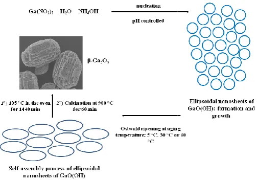
example that could be given is shown in Figure 4a, where the luminescence properties were studied using the excitation wavelength of 370 nm (Horiba Jobin Yvon, model Fluorolog FL3-122). A broad and intense blue emission band appeared for the ellipsoidal -Ga2O3
condensation technique. A solution containing Ga(NO3)3.xH2O, deionized water, and NH
prepared and kept at a medium of pH 9 under continuous magnetic stirring for 30 minutes; in a reflux condenser, the new solution could be refluxed at 60 °C for 12 h, later decanted and washed repeatedly with water and ethanol to remove non reactive species, by-products and organic impurities; it could be dried at 70 °C for 5 h, and calcined at 900 ° C for 1 h. It is assumed that the reflux condensation method is a green route for the synthesis of structures that enables the control of their morphology and surface properties (
Avadhani et al., 2013).
Optical, morphological, chemical, and structural characterizations of β-Ga2O3
condensation technique
35827, November, 2019
oxygen vacancy pair by (Vo,VGa) (Kumar and
(r2)
As it was represented in the reactions, the electron is trapped from the donor to the conduction band, and the hole is trapped from an acceptor to the valence band. Broad emission spectrum is ascribed to the donor states, which are derived from oxygen vacancies, thus leading the n-type semiconductor behavior of (Kumar and Singh, 2013; Fu et al., 2003). An example that could be given is shown in Figure 4a, where the uminescence properties were studied using the excitation of 370 nm (Horiba Jobin Yvon, model Fluorolog-3 broad and intense blue emission band appeared synthesized through the reflux condensation technique. A solution containing 0.1 M O, deionized water, and NH4OH could be prepared and kept at a medium of pH 9 under continuous magnetic stirring for 30 minutes; in a reflux condenser, the new solution could be refluxed at 60 °C for 12 h, later decanted and washed repeatedly with water and ethanol to remove
non-products and organic impurities; it could be dried at 70 °C for 5 h, and calcined at 900 ° C for 1 h. It is assumed that the reflux condensation method is a green route for the synthesis of structures that enables the control of their hology and surface properties (Girija, Thirumalairajan,
Rodrigues, AV and Sabino, NL., Gallium Oxide: A Perspective of Features In Photoluminescence And Gas Sensor Applications
Figure 4 FEG-SEM ofβ-Ga2O3and PL behavior under ex of 370 nm: broad
and intense blue emission band for β-Ga2O3 synthesized through reflux
condensation technique, and later calcined at 900 °C (a); β-Ga2O3 ICSD card
no. 83645 and experimental XRD with diffraction peaks indexed within the
orthorhombic structure with space group (b); EDS of ellipsoidal
β-Ga2O3 (c).
In Figure 4a, the morphology of the particles was studied using a field emission gun scanning electron microscope equipped with an X-ray energy dispersive spectrometer (EDS). The FEG-SEM (FEG-SEM; JEOL, model JSM-7500F) showed the morphological characteristics of the material: the particles were found to be ellipsoidal and composed of parallel sheets. Finding in Figure 4b, the diffraction peaks (XRD; RIGAKU RINT-2000; Cu Kα radiation at a scan rate of 5 °C/min, with 2 θ from 7 to 90°, D/teX Ultra; PSD) were fully indexed in the monoclinic structure (ICSD card no. 83645), and the cell parameters correspondent to a = 12.2140 Å, b = 3.0371 Å, c = 5.79810 Å, and β = 103.83 Å, which are in agreement with other results in the literature (Rodrigues and Sabino, 2019; Shan et al., 2017; Kumar, Sarau, Tessarek et al., 2014; Xu et al., 2015). In EDS (Figure 4c), a qualitative chemical analysis of the particles was performed, exhibiting Ga and O peaks from the particles, as well as Si peak from the substrate.
Emissions at the red range of the wavelength are rarely observed in -Ga2O3, whose achievement is explained by the incorporation of N or other foreign impurities during the high temperature heating process in the ambient air. The N impurities act as acceptors, which encourage the hole capture that recombines with electrons captured at oxygen vacancy donors (Abdullah, Yam, Mohmood et al., 2016; Zhang, Lin, Zhang et al., 2013). In order to facilitate the incorporation of N impurities, several techniques can be applied. The literature mentioned some of these techniques as followed: synthesis of N-doped -Ga2O3 through microwave plasma enhanced chemical vapor deposition (Chang, Lu, Chen et al., 2011); growth of -Ga2O3 nanostructures through thermal annealing of gold coated GaAs wafers in N2 atmosphere (Jangir et al., 2011); annealing of as-prepared particles under NH3 flow with N doping variation (Zhang, Lin, Zhang et al., 2013); melt of Ga in air atmosphere under higher temperatures, creating high vapor pressure that is suitable for incorporation of N from ambient air (Vanithakumari and Nanda, 2009); growth of -Ga2O3 via chemical vapor deposition (Kumar, Sarau, Tessarek
et al., 2014; Kumar, Kumar, and Singh, 2014; Kumar, Tessarek, Christiansen et al., 2014); heat of small gallium metal ingots in conventional tube furnace with Ar gas flow (Khan, Jadwisienczak, and Kordesch, 2006); sintering of the -Ga2O3 single crystals by floating zone technique (Zhang, Li, Xia et al., 2006); growth of Ga2O3 nanobelts through thermal evaporation of GaN and nitridation at high temperature by NH3 (Abdullah, Yam, Hassan et al., 2013); synthesis of the N-doped
-Ga2O3 nanowires through facile vapor-transport and condensation method (Chang, Yeh, Li et al., 2009).
Exhibiting a photoresponse under 254 nm UV light irradiation, the solar-blind ultraviolet characteristic can also be observed in a thin film of α-Ga2O3, having larger band gap than β-Ga2O3, with a value of 5.15 eV. Besides the increase of photocurrent has been observed, the rise of both optical input power and applied bias has also been related by some authors. Herein, it can be indicated that there is a potential application in solar-blind photodetectors (Guo et al., 2016).
Techniques of Gallium Oxide Synthesis, Mechanisms of Gas Sensitivity, And General Applications
1D Ga2O3 nanostructures could be synthesized through several methods that need operation temperature around 1300 °C or even 1600 °C. Thermal evaporation, thermal annealing, chemical vapor deposition, arc-discharge, carbothermal reduction laser ablation, oxidation of milling GaN, microwave plasma, and catalyst-assisted are some of these techniques, which involve complex procedures that influence the purity of the materials. The electron beam evaporation (e-beam) technique is similar to the thermal evaporation, differing only by an electron beam instead of thermally heating the source via tungsten filament. The electron beam evaporation is much used in deposition of various materials for several applications. The β-Ga2O3 synthesis has been used the alumina template to facilitate the achievement of their so-called nanostructures, e.g. nanotubes and nanowires. As long as the soft-chemistry routes at low temperatures have advantages of being economical, energy efficient and environmental friendly, these procedures have been attracted much attention for the 1D materials’ development. Microelectronics, catalysis, coatings, energy storage, and environment protection are some of the technological applications that generally use nano-oxides (Makinudin et al., 2017; EL-Sayed et al., 2011).
International Journal of Recent Scien
electrospinning are also techniques used to successfully achieve the Ga2O3 development (Sun et al., 2017). A scheme of the formation process of ellipsoidal β-Ga2O
reflux condensation and direct precipitation techniques is depicted in Figure 5. The morphologies of the GaOOH precursor and final product of β-Ga2O3 are shown, which demonstrated that the steps to obtain that materials are the same when using both techniques.
Formation steps of ellipsoidal β-Ga2O3
reflux condensation and direct precipitation techniques
Figure 5 Scheme of the formation process of ellipsoidal β
through reflux condensation and direct precipitation techniques.
In general, direct metal oxide formation of nanostructures is applied in hydrothermal synthesis, which is the most convenient and practical technique that avoids special instruments, complicated processes and severe preparation conditions. The hydrothermal technique can control the homogeneity, particle size, chemical composition, phase and morphology of the final products. Dissolving precursor metal salts and complexes in water (hydrothermal) or in a solvent (solvothermal), and heating them to high tempera
under pressure in sealed vessels (e.g. autoclaves), the nucleation and growth of nanoparticles occur through the chemical reaction usually between 6 and 48 hours. Generally, nanoparticles with pure and crystalline structures with wider size distribution are produced. Due to its huge advantage of being simple, lower-cost, and facile regarding the achievement of products with higher purity, the hydrothermal method has great potential to industrial applications. Related to the recent scientific researches, the one-dimensional nanostructures of metal oxide can exhibit unique properties, which are not observed in bulk materials due to the controlled motion of electron in limited dimensions (Mirzaei and Neri, 2016; Abdullah, Yam, Mohmood et al. 2016; Zhao
2012; Cao et al., 2015). Combining hydrothermal or solvothermal syntheses with sol-gel, microemulsion, or colloid precipitates as precursors, for instance, the desired nanostructures can be achieved. Moreover, it is likely to synthesize anhydrous, crystalline or amorphous products by controlling the hydrothermal temperatures (
2016). Either sol-gel or arc-discharge enable the synthesis of so-called nanostructures (Makinudin et al., 2017)
the literature, gallium oxide or gallium oxide hydroxide nanostructures produced through non-hydrothermal routes are
International Journal of Recent Scientific Research Vol. 10, Issue, 11(B), pp. 35816-35827, November, 2019
electrospinning are also techniques used to successfully , 2017). A scheme of O3 particles through recipitation techniques is depicted in Figure 5. The morphologies of the GaOOH are shown, which demonstrated that the steps to obtain that materials are the same
particles through reflux condensation and direct precipitation techniques
Scheme of the formation process of ellipsoidal β-Ga2O3 particles
through reflux condensation and direct precipitation techniques.
In general, direct metal oxide formation of nanostructures is applied in hydrothermal synthesis, which is the most convenient and practical technique that avoids special instruments, complicated processes and severe preparation technique can control the homogeneity, particle size, chemical composition, phase and morphology of the final products. Dissolving precursor metal salts and complexes in water (hydrothermal) or in a solvent (solvothermal), and heating them to high temperature and under pressure in sealed vessels (e.g. autoclaves), the nucleation and growth of nanoparticles occur through the chemical reaction usually between 6 and 48 hours. Generally, nanoparticles with pure and crystalline structures with wider bution are produced. Due to its huge advantage of cost, and facile regarding the achievement of products with higher purity, the hydrothermal method has great potential to industrial applications. Related to the recent dimensional nanostructures of metal oxide can exhibit unique properties, which are not observed in bulk materials due to the controlled motion of (Mirzaei and Neri, 2016; Zhao, Song, Fang et al. Combining hydrothermal or
gel, microemulsion, or colloid precipitates as precursors, for instance, the desired nanostructures can be achieved. Moreover, it is likely to anhydrous, crystalline or amorphous products by controlling the hydrothermal temperatures (Mirzaei and Neri, discharge enable the synthesis of , 2017). According to lium oxide or gallium oxide hydroxide hydrothermal routes are
thread-like or belt-like, which are much longer in length and much smaller in width than that synthesized through hydrothermal techniques (EL
this thermal treatment often involves longer period of synthesis. For this reason, the microwave
hydrothermal method has a number of advantages, such as higher reaction rate, rapid volumetric heating which favors the achievement of the desired temperature in a short time, higher yields of products, and energy savings. Comparing with the conventional hydrothermal technique, more nuclei with a narrow size distribution can be formed using the microwave assisted hydrothermal method, which
high heating rate and homogeneous temperature distribution. Thus, fewer nuclei with broader size distribution can be synthesized (Bogdal, D. 2005; Liang
Electrospinning is considered the most versatile technique for generating long fibers with ranging from nanometers to micrometers, being able to manipulate nanofiber composition, synthesize ultra-fine fibers, and tune their high surface area to volume ratio and porosity. The electrospun materials used to form uniform fibers are related to be organic, inorganic, and hybrid polymers as organic-inorganic composites (Wang, Hou, Quan et al., 2009; Zhao, Zhang, Xie
the synthesis of one-dimensional materials with different compositions, this technique is more simple, convenient and cost-effective than chemical or physical vapor deposition, solution, laser ablation, arc discharge, vapor
and template-based methods (Wang, Hou,
As-prepared solutions could be carried out by dissolving 15 wt% polyvinylpyrrolidone (PVP, Sigma
1,300,000) in the mixed distilled water and ethanol with the weight ratio of 1:1, in the vigorous stirring for 3 h at room temperature. Into this solution, 0.1 g Ga(NO
Aldrich) was added, keeping the vigorous stirring for 10 h. The desired solution’s viscosity was achieved. Then, this
was inject into a plastic syringe equipped with stainless needle (18 inch), which was connected with a peristaltic pump, where the flow rate of the solution reached 0.035 mL min connected stainless needle was linked to a high voltage supply as 20 kV, and a plate of aluminum foil was placed with a distance of 15 cm from the needle
nanofibers were dried at 70 °C for 5 h and calcined at 900 °C in air for 1 h, and the temperature heating rates were 1, 5 and 10 °C per min, aiming the formation of β
is known that strong emissions could be appeared with large band widths from 400 to 750 nm, depending on the defects created into the matrix synthesized through the electrospinning technique during the temperature annealing processes. The nanofibers could exhibit smaller fiber d
solvent (ethanol) (Rodrigues and Sabino, 2019).
Regarding the sol-gel technique, alkaline metal oxides, organic and inorganic salts are used as precursor materials in organic or aqueous solvents with catalysis, stabilizers, and
This method has the advantage of being faster process at low temperatures that reduces the possibility of parasitic phase formation, and it uses the water
than the one which applies organic solvents that combin toxicity and high vapor pressure (Mirzaei and Neri, 2016). Sol gel precursor solution is used to synthesize Ga
and nanotubes through the electrospinning method. The Ga
35827, November, 2019
like, which are much longer in length and much smaller in width than that synthesized through hydrothermal techniques (EL-Sayed et al., 2011). However, this thermal treatment often involves longer period of synthesis. For this reason, the microwave-assisted hydrothermal method has a number of advantages, such as higher reaction rate, rapid volumetric heating which favors the he desired temperature in a short time, higher yields of products, and energy savings. Comparing with the conventional hydrothermal technique, more nuclei with a narrow size distribution can be formed using the microwave-assisted hydrothermal method, which is explained by a very high heating rate and homogeneous temperature distribution. Thus, fewer nuclei with broader size distribution can be
; Liang et al., 2014).
Electrospinning is considered the most versatile technique for generating long fibers with ranging from nanometers to micrometers, being able to manipulate nanofiber composition, fine fibers, and tune their high surface area to o and porosity. The electrospun materials used to form uniform fibers are related to be organic, inorganic, and inorganic composites (Wang, Hou, , 2009; Zhao, Zhang, Xie et al., 2011). Regarding mensional materials with different compositions, this technique is more simple, convenient and effective than chemical or physical vapor deposition, solution, laser ablation, arc discharge, vapor-phase transport, based methods (Wang, Hou, Quan et al., 2009). prepared solutions could be carried out by dissolving 15 wt% polyvinylpyrrolidone (PVP, Sigma-Aldrich, Mw 1,300,000) in the mixed distilled water and ethanol with the weight ratio of 1:1, in the vigorous stirring for 3 h at room emperature. Into this solution, 0.1 g Ga(NO3)3.xH2O (Sigma-Aldrich) was added, keeping the vigorous stirring for 10 h. The desired solution’s viscosity was achieved. Then, this solution was inject into a plastic syringe equipped with stainless needle nch), which was connected with a peristaltic pump, where the flow rate of the solution reached 0.035 mL min−1. The connected stainless needle was linked to a high voltage–power supply as 20 kV, and a plate of aluminum foil was placed with cm from the needle tip. The as-prepared nanofibers were dried at 70 °C for 5 h and calcined at 900 °C in air for 1 h, and the temperature heating rates were 1, 5 and 10 °C per min, aiming the formation of β-Ga2O3 fine nanofibers. It issions could be appeared with large band widths from 400 to 750 nm, depending on the defects created into the matrix synthesized through the electrospinning technique during the temperature annealing processes. The nanofibers could exhibit smaller fiber diameter with decreasing solvent (ethanol) (Rodrigues and Sabino, 2019).
Rodrigues, AV and Sabino, NL., Gallium Oxide: A Perspective of Features In Photoluminescence And Gas Sensor Applications
materials with the desirable phase can be synthesized using sols containing gallium precursors, PVP, and ethanol solution. Having high yield, the pure and structurally uniform nanoribbons of Ga2O3 have been successfully synthesized using the as-prepared inorganic-organic composite fibers without catalyst, substrate, or vacuum condition (
Li et al., 2007). In general, size and shape of colloidal nanocrystals can be controlled in situ by adjusting the synthesis conditions, allowing the exploration of quantum confinement, being modified post-synthetically by functi
conjugation with organic or biomolecules, or by forming a composite with polymers or other nanostructures. All of these abilities in combining solid state-like optical and mechanical properties of nanocrystals enable them to the application optical and photonic devices (Stanish and Radovanovic, 2016). The microemulsion technique is used to synthesize metal nanoparticles, metal oxides, semiconductor quantum dots, and polymeric nanoparticles in a range of structures through templating. The technique is a thermodynamically stable dispersion of two immiscible liquids that needs the addition of a surfactant (ionic or nonionic) and/or co-surfactant under some critical concentration in order to form micelles or inverse micelles, which depend on the concentrations of water and organic liquid. Through long reaction times and/or high annealing temperatures to complete their formation, homogeneous, pure, and small particles of metal oxides can be synthesized (Mirzaei and Neri, 2016).
Either pure or doped Ga2O3 are related to fulfill considered requirements for being applied in transparent conducting electrodes, phosphors, gas sensors, dielectric gates, etc (Liu, Yamazaki, Shen et al., 2008). Being applied in metal
semiconductor structures (Ortiz et al., 2001), Ga
insulator at room temperature with forbidden energy gap of around 4.9 eV, and a semiconductor above 500 °C (in some cases, its semiconductor behavior is found above 800 °C). The process of calcination under reducing atmos
the formation of oxygen vacancies, which lead the generation of Ga2O3 n-type semiconductor (Yang, Zhao, and Frost, 2009; Ortiz et al., 2001).
Regarding the gas sensor behavior in mixtures of reducing gases and in reducing gases plus oxygen systems, complicated interactions occur and must be taken into account, once the conductivity change is not a simple sum of the effects of gases (Réti et al., 1994). Either reducing gases (H
oxidizing gases (O2) can be detected by gallium oxide at higher temperatures, and show gas selectivity by controlling the temperature measured (Ogita et al., 2003; Bausewein 1997). According to the literature, Ga2O3 thin films exhibit n type semiconducting properties above 600 °C. At temperat below 700 °C, the n-type is sensitive to reducing gases. In this case, the adsorbed oxygen ions react with the reducing gases, releasing the electrons and decreasing the sensor resistance. Above 900 °C, the n-type Ga2O3 is operated as oxidizing sensor. Here, the atmospheric oxygen is adsorbed in an ionized form at the surface of the material, with the ionization taking place by capturing free-charge carriers from the n semiconductor oxide, leading to an increase of the electrical resistance of the Ga2O3 sensor sensing layer (
et al., 2016; Swamy, Shafirovich, and Ramana, 2013; Majewski, and Aldinger, 2002). Thus, electrical properties of
Gallium Oxide: A Perspective of Features In Photoluminescence And Gas Sensor Applications
materials with the desirable phase can be synthesized using sols taining gallium precursors, PVP, and ethanol solution. Having high yield, the pure and structurally uniform have been successfully synthesized organic composite fibers uum condition (Zhang, Yang, , 2007). In general, size and shape of colloidal nanocrystals can be controlled in situ by adjusting the synthesis conditions, allowing the exploration of quantum confinement, synthetically by functionalization and conjugation with organic or biomolecules, or by forming a composite with polymers or other nanostructures. All of these like optical and mechanical properties of nanocrystals enable them to the applications in Stanish and Radovanovic, 2016). The microemulsion technique is used to synthesize metal nanoparticles, metal oxides, semiconductor quantum dots, and polymeric nanoparticles in a range of structures through he technique is a thermodynamically stable dispersion of two immiscible liquids that needs the addition of surfactant under some critical concentration in order to form micelles or inverse n the concentrations of water and organic liquid. Through long reaction times and/or high annealing temperatures to complete their formation, homogeneous, pure, and small particles of metal oxides can be
are related to fulfill considered requirements for being applied in transparent conducting electrodes, phosphors, gas sensors, dielectric gates, etc (Liu, , 2008). Being applied in
metal-insulator-, 2001)metal-insulator-, Ga2O3 is an insulator at room temperature with forbidden energy gap of around 4.9 eV, and a semiconductor above 500 °C (in some cases, its semiconductor behavior is found above 800 °C). The process of calcination under reducing atmospheres facilitates the formation of oxygen vacancies, which lead the generation type semiconductor (Yang, Zhao, and Frost, 2009;
Regarding the gas sensor behavior in mixtures of reducing oxygen systems, complicated interactions occur and must be taken into account, once the conductivity change is not a simple sum of the effects of gases (Réti et al., 1994). Either reducing gases (H2, CO, CH4) or ium oxide at higher temperatures, and show gas selectivity by controlling the , 2003; Bausewein et al.
thin films exhibit n-type semiconducting properties above 600 °C. At temperatures
type is sensitive to reducing gases. In this case, the adsorbed oxygen ions react with the reducing gases, releasing the electrons and decreasing the sensor resistance. is operated as oxidizing . Here, the atmospheric oxygen is adsorbed in an ionized form at the surface of the material, with the ionization taking charge carriers from the n-type semiconductor oxide, leading to an increase of the electrical sensor sensing layer (Wang, Wang, Sun , 2016; Swamy, Shafirovich, and Ramana, 2013; Taş, , 2002). Thus, electrical properties of
the n-type at elevated temperatures, e.g. insulator
transistor behavior, are led by oxygen deficit in the crystal lattice. Between 800 and 1000 °C, there is a rapid crystal defect equilibrium with the oxygen content of the ambient atmosphere. In case of oxygen vacancies excess, these contents are like shallow donors in n
Giber, and Meixner, 1992; Xiang, Zhou, and Wang, 2017). According to the literature, there is also a possibility to dope Ga2O3 with groups I and II metals from
to have p-type conductivity (Chikoidze
sense, the metal oxides conductivity changes as a function of the oxygen partial pressure due to an equilibrium that is established between the oxygen vacancies of the mater the externally prevailing oxygen partial pressure. At lower temperatures, Ga2O3 cannot detect oxygen partial pressure anymore because the defect equilibrium is frozen. The use of some donor or acceptor metallic additives as catalysts can help the improvement of signal evaluation in order to accelerate the conversion of the gases at the gallium oxide surface. Since the catalyst is selected and the material reaction responds to a specific gas, the material with selectivity is then achieved (Bausewein et al. 1997). So far, there are three gas sensitive mechanisms which explain the electrical conductivity (Hoefer, Frank, and Fleischer, 2001). These mechanisms are depicted in Figure 6.
Mechanisms of the gas sensitivity involving Ga
Figure 6 Mechanisms of the gas sensitivity involving Ga
reducing gas (a), surface defects (b), and bulk defects (c). Figure modified from the literature (Hoefer, Frank, and Fleischer, 2001).
Gallium Oxide: A Perspective of Features In Photoluminescence And Gas Sensor Applications
at elevated temperatures, e.g. insulator-to-metal transistor behavior, are led by oxygen deficit in the crystal lattice. Between 800 and 1000 °C, there is a rapid crystal defect equilibrium with the oxygen content of the ambient en vacancies excess, these contents are like shallow donors in n-type semiconductor (Fleischer, Giber, and Meixner, 1992; Xiang, Zhou, and Wang, 2017). According to the literature, there is also a possibility to dope with groups I and II metals from the Mendeleyev table type conductivity (Chikoidze et al., 2017). In this sense, the metal oxides conductivity changes as a function of the oxygen partial pressure due to an equilibrium that is established between the oxygen vacancies of the material and the externally prevailing oxygen partial pressure. At lower cannot detect oxygen partial pressure anymore because the defect equilibrium is frozen. The use of some donor or acceptor metallic additives as catalysts can help mprovement of signal evaluation in order to accelerate the conversion of the gases at the gallium oxide surface. Since the catalyst is selected and the material reaction responds to a specific gas, the material with selectivity is then achieved 1997). So far, there are three gas sensitive mechanisms which explain the electrical conductivity (Hoefer, Frank, and Fleischer, 2001). These mechanisms are depicted in
Mechanisms of the gas sensitivity involving Ga2O3
Mechanisms of the gas sensitivity involving Ga2O3: chemisorption of the
International Journal of Recent Scientific Research Vol. 10, Issue, 11(B), pp. 35816-35827, November, 2019
Regarding the sensor and catalyst applications, large surface area to volume ratio can influence significantly their results due to the size-dependent reactivity and interactions of the Ga2O3 with other atoms and molecules of the environment where the material analyzed is surrounded. In general, the materials size-dependence has been taken into account for being applied in new biophysical sensors, thermoelectronic, nanoelectronic, and nanophotonic devices (Yang, Zhao, and Frost, 2009; Meléndrez, Cárdenas, and Arbiol, 2010). In order to enhance the surface area and increase a reaction rate, microstructures are preferable in photoelectrodes of photoelectrochemical cell and photocatalysis. For solar cell applications, low deposition temperature is required to reduce a production cost and keep a good interface quality. Large-scale deposition is also important for these photoelectrodes, photocatalysis and solar cell devices (Fleischer and Meixner, 1991). Moreover, the enhanced absorption of light in thin photodetectors and organic solar cells can be achieved through the replacement of amorphous silicon and thin-doped indium oxide by Ga2O3 (Xiang, Zhou, and Wang, 2017; Meléndrez, Cárdenas, and Arbiol, 2010). It is also related that the Ga2O3 semiconductor presented photocatalytic behavior under UV-C light, finding the degradation of gaseous benzene and some derivates under dry flow, i.e. aromatic hydrocarbon pollutants and typically volatile organic compounds present in urban and confined atmospheres. The photocatalytic activity of α-, β-, γ- and δ-Ga2O3 degrades these aromatic hydrocarbon pollutants, and it changes with the semiconductor surface area, crystallinity, pore, geometric structure, and electronic properties face to the gas-phase oxidation of aromatic hydrocarbons. It means that the photocatalytic activity strongly depended on the Ga2O3 polymorph nature (Jędrzejczyk et al., 2017).
Thin films of Ga2O3 with stable grain size of about 100 nm are successfully produced through high-frequency magnetron sputtering technique using a target made of Ga2O3 ceramics, where the films are deposited on non-conducting BeO ceramic substrates (Fleischer and Meixner, 1991). Ga2O3 thin film growth is also possible through MOCVD as followed: polycrystalline -Ga2O3 and amorphous gallium oxides are described to be successfully deposited on crystalline silicon substrates (c-Si) at temperatures over 500 °C; -Ga2O3 has been fabricated on m- and r-plane sapphire substrates at a temperature of 650 °C; and -Ga2O3 and -Ga2O3 have been synthesized under epitaxial growth. As the high temperature processes facilitates the deterioration of the devices qualities and the conversion efficiency of solar cells decreases by increasing the deposition temperature, it is important to investigate low deposition of Ga2O3 (Takiguchi and Miyajima, 2017). It can be mentioned that the atomic layer deposition also allows the Ga2O3 film growth on c-sapphire substrate at considerably lower temperature (Boschi et al., 2016).
Besides these techniques, there are others which achieved great quality of β-Ga2O3 thin films, such as sol-gel, sputtering, pulsed-laser deposition, molecular beam epitaxy, and atomic layer deposition (ALD). The ALD technique accurately controls the film thickness at low temperature, and it enables great conformality and large area uniformity, explaining its attraction in transparent and flexible polymers. An alternative to this technique is the plasma-enhanced ALD (PEALD), which uses the plasma source to create ions and radicals in
order to provide materials that can be deposited at low temperatures (Altuntas et al., 2014).
The potential of the β-Ga2O3 material in being applied as transistors and diodes with simple structures comes from its high breakdown field (Ebr). Very low hole mobility (μ) prohibiting effective p-type conductivity in Ga2O3 is expected from the calculation of the Ga2O3 band structure. It is well-known that the thermal conductivity of Ga2O3 is directly associated with the crystal orientation, once the gallium oxide has an asymmetric crystal structure. The literature has described the highest thermal conductivity of 0.27 W (cm K)-1 obtained in the [010] direction, being approximately twice larger than the respective thermal conductivity of the [100] direction. Comparing the β-Ga2O3 physical properties with the ones of the other semiconductors, its thermal conductivity respective to the [010] direction is still much smaller (Higashiwaki et al., 2016).
Projections
The metal oxides are varied from insulators to superconductors, being widely applied in several fields. As the subject of our recent research, the gallium oxide is an important semiconductor that has potential application in optoelectronic devices. Various synthesis methods are attempt to produce Ga2O3, aiming their nanostructures formation (Quan et al., 2010). In case of gas sensor applications, several processes in industry look for optimization of their management, as well as the cost-effective and stable sensors for different gases. The semiconductivity is based on an oxygen deficiency of the crystal lattice. These oxygen vacancies are ionized, forming donors and trapping electrons in grain boundary levels. Besides, there is a strong modulation of the sensitivity to reducing gases (Frank, Fleischer, and Meixner, 1996). Photodetectors also showed potential to be applied as missile threat detection, secure optical communications, flame monitoring and detection, UV environmental monitoring and biological threat detection, thus operating in the solar blind region from 200 nm to 280 nm. Avoiding the persistent photoconductivity effect, it is related that the photodetectors are based on semiconductor. However, the fabrication of solar blind photodetectors based on narrow band gap semiconductors has shown degradation of the device performance with temperature, needing an optical filter. Therefore, wide band gap semiconductors based solar blind photodetectors have been developed in order to work at high temperature without using optical filters. Unfortunately, these detectors have shown some problems such as low conductivity, large dislocation densities and the crack of the deposited film due to the thermal/lattice expansion mismatches. Thus, some effort must be done to achieve an improvement of a specific application regarding the photosensitivity (Mahmoud, 2016).
Rodrigues, AV and Sabino, NL., Gallium Oxide: A Perspective of Features In Photoluminescence And Gas Sensor Applications
speed spreads the colloid droplets of Au nanoparticles; and high spin provides the adequate outward centrifugal force to overcome the interparticle interactions, avoiding nanoparticle conjugation. The results pointed that the nanowire diameter decreases with increase of separation distance. This diameter also depends on the growth temperature and catalyst nanoparticle size. At high temperature (850-900 °C), however, the diameter does not depend on the catalyst nanoparticle size. Smaller diameter (< 50 nm) can be obtained using lower growth temperature (800 °C) and smaller catalyst nanoparticle size. The band gap of these nanowires also depends on its diameter, increasing from 4.70 to 4.80 eV. Besides these values, XRD and Raman measurements can demonstrate that changes in their respective graphs occur due to the changes in structural strain with nanowire diameter (Kumar, Kumar, and Singh, 2017).
CONCLUSIONS
Inorganic semiconductors as gallium based (Ga2O3 compounds) are promising candidates that have advantages over organic materials for optoelectronic and electronic devices’ applications. They have different crystalline phases, such as α-, β-, γ-, δ-, and ɛ-Ga2O3, where the chemical and thermodynamic stabilities are more appreciative for the monoclinic structure β-Ga2O3, whose band gap values are between 4.4 and 4.9 eV at room temperature. Due to their conduction and photluminescence properties, Ga2O3 are enabled to be applied in water splitting, photocatalysis, gas sensing, nanophotonics, tunable phosphorescence, plasmonics, and other several fields. The conductivity of the Ga2O3 n-type is extremely sensitive to reducing atmospheres. Its n-type semiconductor feature comes from the oxygen vacancies. Different interaction mechanisms between the sensor and the target gas are led by the type of the gas used: under an oxidative atmosphere there is an increase of the electrical resistance of the sensor sensing layer (Ga2O3), and under a reducing atmosphere there is a decrease of the sensor resistance. The photoluminescence behavior of the Ga2O3 nanocrystals is influenced by thermal treatments, average pore sizes, and specific surface areas. Both blue and UV emissions are attributed to the donor-acceptor transitions, which involves oxygen vacancies, thus correlating the existence of electrical conductivity. For green emission, there are self-trapped or bound excitons. Herein, very broad, intense and visible Ga2O3 emission band in the range of the wavelength are characteristics that enable Ga2O3 to optoelectronic applications. Various methods of the gallium oxide production have been studied as a pathway to carry out their nanomaterials, taking into account their facile, non-expensive, and simple process of synthesis, besides being environmentally friendly. The advantages of photoluminescence and gas sensor applications come from the large surface area to volume ratio of the Ga2O3 materials. The synthesis method, precursors used, annealing temperature, solvent, precipitant, dispersing agent, and other factors also influence both optical and electrical properties. As the Ga2O3 conduction properties depend on its diameter, these materials with smaller diameter than the depletion layer width are completely depleted whereas Ga2O3 with larger diameter have a conduction channel. Additional researches based on the influences of the environment, and donor and acceptor type dopants on the surface semiconductor must be proceeded in
order to observe the control of the conductivity, as well as the photoluminescence and gas-sensitivity performances’ improvement of the Ga2O3.
Conflict of Interest
No conflict of interest was reported by the authors. Acknowledgments
The authors acknowledge the Institute of Chemistry of UNESP University for the equipments and lab space. FEG-SEM facilities were provided by the LMA-IQ-UNESP.
References
Abdullah, Q.N., Yam, F.K., Hassan, Z., and Bououdina, M. 2013. Growth and conversion of -Ga2O3 nanobelts into GaN nanowires via catalyst-free chemical vapor deposition technique, Superlattices and Microstructures, 54: 215-224.
Abdullah, Q.N., Yam, F.K., Mohmood, K.H., Hassan, Z., Qaeed, M.A., Bououdina, M., Almessiere, M.A, Al-Otaibi, AL., and Abdulateef, S.A. 2016. Free growth one-dimensional β-Ga2O3 nanostructures including nanowires, nanobelts and nanosheets using a thermal evaporation method, Ceramics International, 42(12): 13343-13349.
Akazawa, H. 2016. Formation of various phases of gallium oxide films depending on substrate planes and deposition gases, Vacuum, 123: 8-16.
Al-khamis, Kh.M., Mahfouz, R.M., Al-warthan, A.A., and Siddiqui, M.R.H. 2009. Synthesis and characterization of gallium oxide nanoparticles, Arabian Journal of Chemistry, 2(2): 73-77.
Altuntas, H., Donmez, I., Ozgit-Akgun, C., and Biyikli, N. 2014. Electrical characteristics of -Ga2O3 thin films grown by PEALD, Journal of Alloys and Compounds, 593: 190-195.
Bartic, M. 2016. Mechanism of oxygen sensing on -Ga2O3 single-crystal sensors for high temperatures, Physical Status Solidi A, 213(2): 457-462.
Bausewein, A., Hacker, B., Fleischer, M., and Meixner, H. 1997. Effects of palladium dispersions on gas-sensitive conductivity of semiconducting Ga2O3 thin film ceramics, Journal of the American Ceramic Society, 80(2): 317-323.
Binet, L., and Gourier, D. 1998. Origin of the blue luminescence of -Ga2O3, Journal of Physics and
Chemistry of Solids, 59(8): 1241-1249.
Blasse, G., and Bril, A. 1970. Some observations on the luminescence of -Ga2O3, Journal of Physics and
Chemistry of Solids, 31(4): 707-711.
Boschi, F., Bosi, M., Berzina, T., Buffagni, E., Ferrari, C., and Fornari, R. 2016. Hetero-epitaxy of -Ga2O3 layers by MOCVD and ALD, Journal of Crystal Growth, 443: 25-30.
Bogdal, D. 2005. Microwave effect vs. thermal effect, 25, 14-21. Bäckvall, J.E., Baldwin, J.E., and Williams, R.M. (eds.). 2005. Microwave-assisted organic synthesis: one hundred reaction procedures, Elsevier Science, Oxford. Calestani, D., Alabi, A.B., Coppedè, N., Villani, M.,