Simulation and Experimental Validation of
Common Mode Voltage in Three Phase Induction
Motor Driven by Five Level Inverter Using PIC
Microcontroller
Reddy Sudharshana K and V Muralidhara
EEE, SET, Jain University, Bangalore, India Email: {reddy3690, v.muralidhara.1952}@gmail.comA Ramachandran and R Srinivasan
Vemana Institute of Technology, Bangalore, IndiaEmail: {arama1947, rsrini47}@gmail.com
Abstract—The Induction Motor is considered to be a constant speed motor. Squirrel-cage induction motors are widely used in industrial applications. Due to the advancement in power electronics and in microprocessor technology the speed of the Induction Motor can be varied within certain limitations. There are many methods to control and run the induction motor in Variable speed drive applications. The speed of an induction motor can be varied by changing the frequency of the AC voltage applied on the stator. The amplitude of the AC voltage applied on the stator should be proportional to the frequency, to maintain a constant air gap flux. Speed of an induction motor can be controlled by maintaining the voltage to frequency ratio constant. The method of V/f control gives good performance under steady-state, which is sufficient for motor drive industrial applications. The basic method is 2-level inverter controlled by the microcontroller using the space vector modulation method. By this method the output of the inverter will be Non- sinusoidal and hence at the star point of the load there exists a Voltage with respect to ground and it is known as Common Mode Voltage, which produces electromagnetic interference. To lower the Common Mode Voltage a higher level of inverter can be used. By using the 5-level inverter the common mode voltage can be minimized when compared to 2-level and 3-level inverter. In this paper the authors have discussed the 5-level inverter driving the induction motor by simulation using MATLAB-Simulink and by Experiment. Fast Fourier transform has been done using the signal Analysis software and results are plotted with frequency versus voltage. The Common Mode Voltage is measured using Agilent make mixed signal oscilloscope. In the conclusion, the result of 5-level inverter common mode voltage is compared with 3-level and 2-level inverter values are compared with different operating frequencies of Induction Motor is shown in the table.
Index Terms—common mode voltage, induction motor, three phase voltage source 2/3/5-level inverter, pulse width modulation, space vector modulation
Manuscript received July 31, 2018; revised December 12, 2018.
I. INTRODUCTION
The Common Mode Voltage (CMV) exists at the star point of the Induction Motor (IM) in three phase inverter using Space Vector Modulation (SVM) technique. The output of the Voltage Source Inverter (VSI) will be non-sinusoidal. The existence of CMV has been reported by B. Muralidhara [1], [2]. In addition, due to the asymmetrical flux through the arbour line loop induces CMV. A. Muetze [3] reports the High-Frequency (HF) component that exists at the CMV. Hence it is necessary to minimize the CMV within limits [4] so that there will be minimized Electromagnetic Interference (EMI) and the insulation problem of the winding.
In industrial applications the three phase 2-level and 3-level inverter is widely used in variable speed IM drive systems using VSI which produce three phase AC output voltage of desired amplitude and frequency from a fixed DC voltage source. In 2/3/5-level inverter, the output waveform of inverter is stepped square wave. The output waveform of an inverter should be sinusoidal for efficient operation. The complexity of circuit is more in higher level inverter. A. Nabae [5] in 1981 discussed the Multilevel Inverter (MLI) concept. The advantages are with low switching losses with reduced EMI and with better power quality. The drawbacks for higher level inverters are complexity in circuits, the number of switching devices and various DC voltage levels. The PIC microcontroller [6] has been used to generate gate pulses for the 5-level inverter as per the Hexagon of space vector modulation [7], [8]. The drive circuit is interfaced with necessary opto-isolation modules and three phase H-bridge circuit is used to drive the switching devices.
and load combinations. In three phase AC loads, the phase to ground voltages can be written as the sum of the phase voltages and the voltage across the star point of the load to the common ground of the source power supply. The sum of all three phase-to-neutral voltages is zero in a three phase sinusoidal balanced system; the voltage from the star point of load to common ground can be defined in terms of phase to ground voltage as shown in Fig. 1 and (1)-(5).
Figure 1. Inverter fed IM to measure common mode voltage.
VA-n= VAN + VN-n (1)
VB-n= VBN + VN-n (2)
VC-n= VCN + VN-n (3)
For balanced 3 phase system, ΣV = 0
VAN + VBN+ VCN =0 (4)
VN-n = [(VA-n + VB-n + VC-n) / 3] (5)
III. SPACE VECTOR MODULATION
The experimental work uses the Space Vector Modulation (SVM) method, which produces the output voltage by using the three nearby output vectors. When one of the reference vector moves from one sector to another, results in an output vector abrupt change. In addition it is necessary to find the switching patterns and switching time of the states at each change of the reference voltage. The main advantages are to overcome the variation in DC bus voltage, the ratio V/f of IM is maintained constant by compensating for regulation in inverters. The three phase voltages are
Va = Vm Sinωt (6)
Vb = Vm Sin(ωt-2π/3) (7)
Vc = Vm Sin(ωt-4π/3) (8)
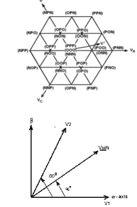
SVM is a better technique for generating a fundamental output (~sine wave) that provides a higher output voltage to the three phase IM and less Total Harmonic Distortion (THD) when compared to sinusoidal PWM. The switching vectors Hexagon for 2/3/5-level are shown in the Fig. 2-Fig. 4.
The basic circuit of the 5-level Neutral Point Clamped (NPC) inverter is shown in Fig. 5. The switching state of each phase of the inverter is listed in Table I. The output space vector voltage is identified by the combination of switching states P2, P1, O, N1 or N2 of the three legs of Fig. 6. For example, in the case of P2, O, N1, the output terminals ‘a’, ‘b’ and ‘c’ have the potentials Vdc/2, 0, and
–Vdc/4 respectively. Since five types of switching states
exist in each leg, a 5-level inverter has 53 = 125 switching states, as indicated in the space vector diagram Shown in Fig. 6. The output voltage vector can assume only 61 discrete positions because some switches are redundant and create the same space vector [9]-[12]. Only the outer most space vector (24) is considered since all the other inner vectors are not considered due to redundancy.
Figure 2. Switching vectors and sectors for 2-level inverter
.
Figure 3. Switching vectors for 3-level inverter and Sampled reference vector in sector-1
Figure 5. Circuit diagram of NPC 5-level inverter
Figure 6. Simulation circuit of NPC 5-level inverter
The basic circuit of the 5-level NPC inverter [13] is shown in Fig. 5. The switching state of each phase of the inverter is listed in Table I. The output space vector voltage is identified by the combination of switching states P2, P1, O, N1 or N2 of the three legs of Fig. 4.
For example, in the case of P2, O, N1, the output terminals ‘a’, ‘b’ and ‘c’ have the potentials Vdc/2, 0, and
–Vdc/4 respectively. Since five types of switching states
exist in each leg, a 5-level inverter has 53 = 125 switching states, as indicated in the space vector diagram Shown in Fig. 4. The output voltage vector can assume only 61 discrete positions because some switches are redundant and create the same space vector [12]. Only the outer most space vector (24) is considered since all the other inner vectors are not considered due to redundancy.
TABLE I. SWITCHING STATES OF 5-LEVEL NPCINVERTER
IV. PROPOSED WORK
Simulation circuit and experimental circuit of 5-level inverter shown in Fig. 5, Fig. 6 with 24 devices using SVM for the speed control of three phase IM is reported. The 2 and 3-level inverter results are taken from the published results [14], [15]. The CMV, phase voltage, line voltage, sum of phase current and phase current are measured using Agilent Mixed Signal Oscilloscope (MSO) associated with Hall sensor, Current probes etc., Simulation has done using MATLAB SimuLink
.
A. Experimental Setup
In the experimental circuit uses MOSFET’s (2SK962) as switching devices with high frequency anti parallel fast recovery diodes is used between drain and source of the MOSFET. The PIC-Microcontroller (16F877) is programmed to generate the gating pulses to the MOSFET’s with proper opto-isolation circuits. 6N139 IC is used as an opto-isolator with isolated DC (+15V) power supply. The DC supply to the 5-level inverter is given using 3-phase Converter with filtering capacitor and Line Impedance Stabilization Network is used to block the unwanted noise signal voltage. DC link high voltage (1200V) capacitor (50μF) has been used. The necessary FFT analysis has done in simulation using MATLAB/ Simulink and for the experimental results using Origin Signal Analysis software. The CMV is analyzed for different frequencies (30Hz, 40Hz, 50Hz) for 5-level Inverter and compared with 2-level and 3-level inverter from earlier published [14], [15] results of the same authors.
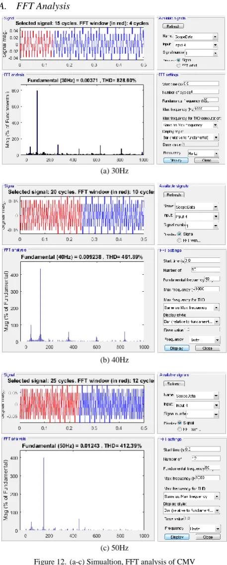
V. SIMULATION AND EXPERIMENTAL RESULTS The pic microcontroller is used for the generation of gating signals for the 5-level NPC inverter shown in Fig. 7. The simulated waveform results are shown in Fig. 8, the experimental results of CMV, Phase Voltage, Line Voltage, Phase Current are recorded using Agilent MSO (500MHz) shown in Fig. 9 to Fig. 11. In CMV, the harmonic frequencies are three times the fundamental frequency. Some harmonics will not produce useable torque, but produces opposing torque and heat, which are harmful to the insulation of IM. In Fig. 12 shows the Simulated FFT analysis of CMV using MATLAB Simulink and in the Fig. 13 shows the FFT analysis of Experimental results using Signal Analysis software for the 30Hz, 40Hz and 50Hz of Operation.
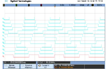
Figure 7. MSO recorded gating signals of 5-level NPC inverter, 40Hz. MODE/
STATE S1 S2 S3 S4 S1
1 S21 S31 S41 V
OUT
P2 1 1 1 1 0 0 0 0 VDC/2
P1 0 1 1 1 1 0 0 0 VDC/4
0 0 0 1 1 1 1 0 0 0
N1 0 0 0 1 1 1 1 0 VDC/4
Figure 8. 40Hz simulated output waveforms of 5-level inverter. Top to bottom: 1; phase voltage, 2; line current, 3; line voltage,
Ch-4; common mode voltage.
Figure 9. Exptl. 30Hz experimental output waveforms of 5-level inverter
Figure 10. Exptl., 40Hz experimental output waveforms of 5-level inverter
Figure 11. Exptl., 50Hz experimental output waveforms of 5-level inverter
Note: For exptl. Fig. 9-Fig. 11), top to bottom: Ch-1; line voltage [200:1], Ch-2; phase voltage [200:1], Ch-3; common mode voltage [200:1], Ch-4; line current [1:1]
A. FFT Analysis
(a) 30Hz
(b) 40Hz
(c) 50Hz
Figure 12. (a-c) Simualtion, FFT analysis of CMV
VI. CONCLUSION
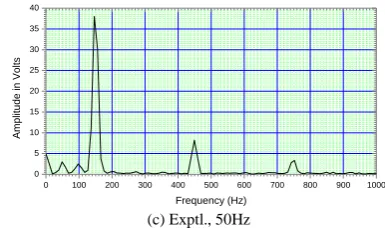
amplitude in 2-level [14], 3-level [15] and 5-level inverter (Fig. 11) is found to be 160VPeak, 142.5Vpeak and
122.5Vpeak respectively for 50Hz of operation.
(a) Exptl., 30Hz
(b) Exptl., 40Hz
(c) Exptl., 50Hz
Figure 13. (a-c) FFT analysis of CMV
Similarly, the FFT analysis of CMV in the experiment for 2-level [14], 3-level [15] and the 5-level inverter is found to be around 45V, 25V and 17V respectively for 40Hz of operation as per the Fig. 13b. Comparing the FFT plots of CMV of the 5-level inverter shows less CMV as per the graph in the Fig. 13a-c. Table II gives the comparison of CMV by simulation and Experimentation for 2, 3 and 5-level inverter. It is found that the 5-level inverter CMV is less when compared to 2 and 3-level inverter. Hence it is concluded that as the number of level increases, the CMV is reduced. In addition, as the number of level increases there will be more number of devices in series, hence the voltage stress on the switching devices gets reduced.
TABLE II. COMPARISON OF RESULTS FOR 2,3 AND 5-LEVEL NPCINVERTER FED INDUCTION MOTOR DRIVE AT DIFFERENT FREQUENCY
parameters 2-level (6 devices)[14] 3-level (9 devices)[15] 5-level inverter (24 devices)
Frequency 30Hz 40Hz 50Hz 30Hz 40Hz 50Hz 30Hz 40Hz 50Hz
CMV(Simulation) 150V 155V 162V 130V 140V 150V 100V 110V 130V
CMV(Exptl.) 140V 151.5V 160V 120V 132V 142.5V 70V 87.5V 122.5V
ACKNOWLEDGMENT
The authors are thankful to KRJS management, Dean, Principal and HoD/ECE of Vemana Institute of Technology, Bangalore. Also thankful to Prof. M.Channa Reddy for his followup with guidance and also to workshop staff for their support in carrying out the fabrication work.
REFERENCES
[1] B. Muralidhara, A. Ramachandran, R. Srinivasan, and M. C. Reddy “Common mode voltage and EMI as the source of disturbance to communication network caused by modern AC motor drive,” Proceedings of 42nd IETE Mid-Term Symposium, Bangalore, India, April 2011, pp. 90–94.
[2] B. Muralidhara, A. Ramachandran, R. Srinivasan, and M. C. Reddy, “Experimental measurement and comparison of common mode voltage, shaft voltage and the bearing current in two- level and multilevel inverter fed induction motor,” International Journal of Information and Electronics Engineering,vol. 1, no. 3, pp. 245-250, 2011.
[3] A. Muetze and A. Binder, “Systematic approach to bearing current evaluation in variable speed drive systems,” Eur. Trans. Elect. Power, vol. 15, no. 3, pp. 217–227, 2005.
[4] C. R. Paul,Introduction to Electromagnetic Compatibility Wiley Series in Microwave and Optical Engineering,John Wiley & Sons, Inc., 1992.
[5] A. Nabae, I. Takahashi, and H. Akagi, “A new neutral-point clamped PWM inverter,” IEEE Trans. Ind. Application, vol. IA 17, pp. 518-523, Sept./Oct. 1981.
[6] Pic Microcontroller (16F877) datasheet.
[7] P. S. Varma and G. Narayanan, “Space vector PWM as a modified form of sine triangle PWM for simple analog or digital implementation,” IETE Journal of Research, vol. 52, no. 6, pp. 435-449, Nov./Dec. 2006.
[8] G. Narayanan and V. T. Ranganathan, “Synchronised PWM strategies based on space vector approach: Principles of waveform generation,” IEEE Proceedings-Electric Power Applications, vol. 146, no. 3, pp. 267-275, May 1999.
[9] B. K. Bose, Power Electronics and Variable Frequency Drives: Technology and Applications,IEEE Press and John Wiley & Sons, Inc., 1997.
[10] IEEE Industry Applications Magazine, ABB Automation Inc., Jul./Aug. 1999.
[11] G. L. Skibinski, R. J. Kerkman, and D. Schlegel, “EMI emissions of modern PWM AC drives,” IEEE Trans. Ind. Application, pp. 47-81, Nov./Dec. 1999.
[12] R. Srinivasan and K. Sundararaman, “Digital control of multi level inverters using simplified space vector modulation,” in Proc. Intl. Conf. on Control Automation, Communication and Energy Conservation, 2009, pp. 1–8.
[13] B. Muralidhara, “An experimental evaluation of 2-level and multilevel inverters used for speed control of IM and study of common mode voltage in both cases,” Ph.D. thesis, JNTU, Aug. 2013.
[14] K. R. Sudharshana, A. Ramachandran, and V. Muralidhara, “Simulation and experimental evaluation of variable speed induction motor drive fed by VSI and study of current harmonics under steady state conditions,” IJEEE, vol. 9, no. 1, Jan.-Jun. 2017.
0 100 200 300 400 500 600 700 800 900 1000
0 2 4 6 8 10 12 14 Frequency (Hz) Am p lit u d e i n Vo lt s
0 100 200 300 400 500 600 700 800 900 1000
0 2 4 6 8 10 12 14 16 18 20 Frequency (Hz) Am p lit u d e i n Vol ts
[15] K. R. Sudharshana, A. Ramachandran, V. Muralidhara, and R. Srinivasan, “Simulation and experimental validation of common mode voltage in induction motor driven by inverter using arduino microcontroller,” presented at the World Congress on Engineering, London, U.K., July 5-7, 2017.
Mr. Reddy Sudharshana K received the B E, and M. E degree in Electrical engineering from Bangalore University, Bangalore .He is working as an Assistant Professor, Vemana I. T., Bangalore- 560034. India. He has guided many Undergraduate students in Power Electronics field. At present pursing for Ph.D. Degree (Research Scholar) with Jain University, Bangalore, India. He is the member of IEEE and ISTE. In his credit he has 5 papers published in reputed International conferences/Journal. (email:[email protected]).
Dr. A Ramachandran obtained his Bachelor’s, Master’s and doctoral Degree in Electrical Engineering from Bangalore University, Bangalore, India. He was with National Aerospace Laboratories Bangalore, India, as scientist in various capacities, and was working in the areas of Power Electronics & drives for the past 41years. He was heading the Instrumentation & controls group of Propulsion Division, and guided many Bachelors and Masters Degree students for their dissertation work. He has also guided Ph.D., for the dissertation work and earlier worked has principal, after superannuation and at present professor ECE department, Vemana I.T.Bangalore-34, having number of papers to his credit both in the national/international Journals / conferences. (email:[email protected]).
Dr. V Muralidhara obtained his B.E, and M.E degrees from University of Mysore and earned Ph.D. from Kuvempu University. He has a teaching experience of over 40 years inclusive of research as a par at of his Ph.D. Started his teaching career at PES College of Engineering Mandya, served there for 6 years and served for 31 years at Bangalore Institute of Technology [BIT], Bangalore and retired from there as Prof. & Head of EEE. Presently working has an Associate Director at Jain University. His area of interest is Power Systems and HV Engineering. In his credit he has 15 papers published in reputed International conferences and one paper in a Journal. At Present he is guiding five doctorate scholar. email:[email protected].