Volume 5, Issue 9, September 2016
3-D Stackable L2 Memory Component Design with NUMA
Architecture
S.Bharath
1,
C.Pamuleti
21
Department of Electronics and Communication,Sreenidhi Institute of Science and
Technology, Affiliated to Jawaharlal Nehru Technological University Hyderabad,Ghatkesar,
Hyderabad, Telangana, 501301.
2
Department of Electronics and Communication, Sreenidhi Institute of Science and
Technology, Affiliated to Jawaharlal Nehru Technological University Hyderabad,Ghatkesar,
Hyderabad, Telangana, 501301.
Abstract---Recently, 2-Dimensional integration technology is
modified in many ways to improve the speed and storage capacity but 3-D dimensional integration technology make the researchers and designers to explore towards the development of advanced architectures in the field of computing systems. Due to the requirement of huge memory in the highly processing systems, like DSPs can be benefited highly from 3-D memory component which is designed using vertically stacking high-density memory under the processing cores. Due to large required memory, tolerance to latency and variations in time for access of memory make L2 memory a suitable option for 3-D integration. In this paper, we present 3-D NUMA, an L2 memory component designed for integration as a 3-D stacked module, which can be attached to a cluster-based multicore platform through its network-on-chip (NoC) interfaces, which offers high-bandwidth for memory access with low average latency. By implementing the memory component with the STM CMOS low-power technology with up to three stacked memory dies (MDs), the 3-D-NUMA is able to deliver a high band width with an average memory access and achieves high clock frequencies.
Index Terms---3-Dimensional integration,synthesizable
3-D-stackable L2 memory, cluster-based multicore platform,network-on-chip.
I.INTRODUCTION
hreedimensional integration has been explored in industry for many years, and a wide variety of technologies, materials, and processes have been used for
research and demonstrations. Several interconnect
technologies have been explored, includingwire bonding,
contactless and through-silicon-via (TSV) vertical
interconnect. Among them, the TSV process of interconnect has gained popularity, due to its high interconnection density. In Future,integration TSV chip market will grow faster than the global semiconductor industry [2]. In addition, wafer foundry technology such as Samsung and TSMC have been developing vertical integration offerings to meet with the demand from leading fabless companies
such as Qualcomm, Broadcom, Marvell and Apple, along with other IC companies. In spite of that, the time for adoption of 3-D integration for bulk production keeps changing into the future. Several technical challenges and
infrastructure issues are delaying high-volume
manufacturing of TSV technology for 3-D ICs. Until these issues can be resolved, alternative packages will continue to be used [3].
Complex system in package (SiP) solutions offered by many companies, addresses a potentially large requirement in the market and are being recognized as the next industry thrust. Heterogeneous integration, system miniaturization and flexibility, and block level testability are some of the several features offered by SiP solutions. In addition to that, they provide a way to integration of planar IC with 3-D IC technology [4]. TSV silicon interposer (TSI) is a good example of how heterogeneous dies with mixed technologies can be integrated at higher levels and greatly reduce die complexity and cost.
In this paper, we present 3-D Stacable L2 memory component designed with NUMA Architecture for integration as a 3-D stacked module, which can be attached to a cluster-based multicore platform through its network-on-chip (NoC) interfaces, offering high-bandwidth for memory access with low average latency. Our proposed component is a synthesizable and scalable NUMA architecture, which allows modular stacking of multiple memory dies (MDs) with identical layouts using a single mask set, supports multiple in-flight transactions, and achieves high clock frequency, because of its highly pipelined nature. Thus implementing the memory IP in STM CMOS-130-nm low-power technology with up tothree stacked Memory Dies. The 3-D-NUMA Architecture is able to transfer a high bandwidth for memory access with an average latency and achieves high clock frequencies.
T
Volume 5, Issue 9, September 2016
II.RELATED WORKS
Advanced IC technologies provide new opportunities for
heterogeneous integration, power delivery, cost
optimization, and thermal management. Among other packaging technologies, dual DRAM package, dual face down, and quad face down with the main target of DRAMs provide complex forms of wire bonding, which may be adopted even for other levels in the memory hierarchy. Technologies, such as TSI [5] and wafer reconstitution [4], provide even more flexibility in hybrid 2.5- D/3-D stacking. TSIs enable stacking of different dies on both sides to achieve a better utilization of space and facilitate heat transfer of high-power chips. Wafer reconstitution provides electrical connections from the chip pads to the interconnects by means of an artificial wafer. Redistributed chip packaging (RCP) [4] developed by Freescale Semiconductor offers scalable chip-scale packaging and multidie heterogeneous integration. In addition, package-on-package stacking is supported in RCP by means of through-package-via.
For 3-D memory stacking, three important research directions have been investigated in the industry and they are: 1) 3- D DRAM main memories; 2) 3-D caches; and 3) 3-D SPMs. 3-D stacked DRAM architecture, where stacked DRAM Architecture for main memory is orthogonal and complementary to this paper. In spite of this, it has some limitations, which has prevented it from being successful in the market so far. Since DRAM dies are not process compatible with logic dies, they have to be manufactured separately and generally by different integrated device manufacturers. This will impose strict requirements and conservative standard rules on the 3-D interfaces such as large TSV size and pitch, and ultrasafe ESD protection circuits and die testing facilities. These requirements result in increased size and cost of the dies, as well as very significant supply chain set up challenges.
On the other hand, 3-D stacking of SRAMs provides more flexibility, opportunities for process optimization, and simplified supply chain, since dies are homogeneous from a technology viewpoint. Needless to say, given their low density and high cost, SRAM-based memories are obviously not a viable DRAM replacement for main memory, and they should be used in lower levels of the memory hierarchy. We should add here that embedding DRAM (eDRAM) memories in the lower levels of memory hierarchy which is also another design alternative for integration. Trigate CMOS eDRAM designed in 22-nm technology by Intel and the 45-nm SOI eDRAM by IBM are two examples, which can offer better area utilization, performance, and even power consumption compared with the SRAM cells in the
III.Dynamic Random Access Memory (DRAM) To Store one bit of data,SRAM require more transistors, which is costlier. DRAM require only one transistor and capacitor to store one bit which is cheaper than SRAM. Embedded DRAM is better choice than SRAM in cost, size and power dissipation.
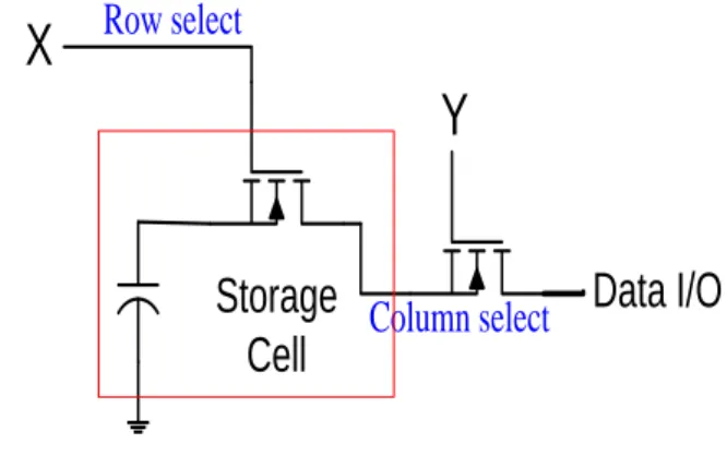
Row select
Column select
Data I/O
Storage
Cell
X
Y
Figure 1. Storage Cell
Here Si02 insulates gate and substrate, creating dielectric
capacitor between gate and substrate. Data bit is stored in this capacitance, such that each bit now only requires 1 MOSFET. However the charge stored in cell dissipates over time and must be recharged over time which need Refreshing process to avoid corruption
A. DRAM Refresh
Must read data bit and write value back to cell.
JEDEC standardises DRAM row refreshes at leastevery 64 ms.
All bits in row must be refreshed.
Dedicated hardware control DRAM refresh Refresh is transparent to user
Above 64 Kbits, DRAM more economic thanSRAM logic
Even with refresh.
B. Write Operation
X Y Data I/O C
Volume 5, Issue 9, September 2016
When both address lines are selected,we can write the data in the memory cell which means in the capacitor of the memory circuit. C. Read Operation Simi larly as write oper ation , whe n both the address lines are selected, we can read the data from the memory cell.
D. DRAM Organisation
DRAM is organised as “row by column” matrix. Matrix stores n 1-bit words. N is determined by the number of address lines available. Each matrix is parallelised to create word size memories. i.e : 8 parallel 4Kx1-bit DRAM matrices creates an 4K * 8-bit RAM module
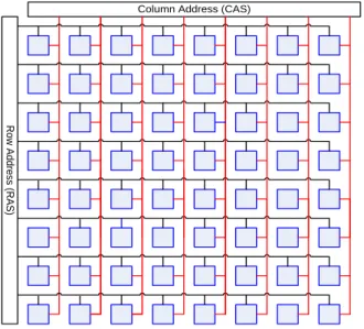
Column Address (CAS)
R o w A d d re s s (R A S )
Figure 2. An 8x8 array forms a 64 x 1 Dynamic RAM The row and column select logic are comprised of address decoders.8-rows and 8-columns need 3-address bits each.Above block is 64x1-bit DRAM. Diagram omits but matrix has 1 data I/O line.Row and Column address control which bit is active
This block can be parallelised to create larger data word.Each bit of data word is read/wrote in parallel
64 x 1 64 x 1 64 x 1 64 x 1 64 x 1 64 x 1 64 x 1 64 x 1
6-Bit Address
Data I/0
MSB LSB
Figure 3. Memory Arrangement
IV.DESIGN IMPLEMENTATION
Physical design of 3-D-NUMA has been performed based on the STM bulk CMOS low-power technology library, with
a multiVTH synthesis. The circuits are implemented in the
Electic Binary and spice code is generated which is used in the LT Spice tool for functional verification in the form of graphical representation.
Figure 4. Single Memory Cell
Figure 5. Inverter Circuit Block
X Y Data I/O C
0 X X C
X 0 X C
1 1 0 0
Volume 5, Issue 9, September 2016
Figure 6. Single 2D Cell.
Figure 7. 2D Cell Read Write Operations
Using the 2D cell, a 8x8 one bit 2D Layer is designed as shown in figure and with the help of that a 3D Layer of 3-bit Memory will be designed, which gives the 3-bit data on selecting a particular location with the help of row and column.
Figure 8. 2D Memory Array
When the spice code is generated in the LT Spice tool,appropriate row and column values, data to every cell,Vdd value have to give in the code. Based on the input values,we get the data values from the corresponding addresses.
Volume 5, Issue 9, September 2016
Figure 10. 3D Memory
Figure 11. 3D Memory Read Write Operations V. CONCLUSION
In this paper, we presented a synthesizable 3-D-stackable L2 memory IP component (3-D-NUMA), which could be attached to a cluster-based multicore platform through its network-on-chip interfaces, offering high-bandwidth for memory access with low average latency.We implemented 3-D-NUMA with STM CMOS-130-nm low power technology. Our design implements a scalable 3-D memory component using NUMA architecture, allows stacking of multiple identical MDs, supports multiple outstanding
transactions, and achieves high clock frequencies due to its highly pipelined nature.
REFERENCES
[1] ErfanAzarkhish,“A Modular Shared L2 Memory Design for 3-D Integration,” IEEE TRANSACTIONS ON VERY LARGE SCALE INTEGRATION (VLSI) SYSTEMS,June 2014.
[2] W. Davis et al., “Demystifying 3D ICs: The pros and cons of going vertical,” IEEE Design Test Comput., vol. 22, no. 6, pp. 498–510, Nov./Dec. 2005.
[3] Yole-Développement. (2012). 3D IC & TSV
Interconnects 2012 Business Update. [Online]. Available:
http://www.i-micronews.com/reports/3dictsv-interconnects-2012-business%-update/8/302/
[4] E. J. Vardaman. (Mar. 2013). 3D IC with TSV: Status
and Developments. [Online]. Available:
http://connection.ebscohost.com/c/articles/86024505/3d-ic-tsv-status-developments
[5] Freescale-Semiconductor. (Jan. 2013). Freescale’s
Redistributed Chip Packaging. [Online].Available: http://www.freescale.com/files/shared/doc/reports_presentat ions/rcppresentation.pdf
[6] A-Star-IME. (Nov. 2010). TSV Silicon Interposer for
High I/O Applications. [Online]. Available:
http://www.ime.a-star.edu.sg/ uploadfiles/3_proposal-tsv-interposer.pdf
[7] E. Azarkhish, I. Loi, and L. Benini, “A high-performance multiported L2 memory IP for scalable three-dimensional integration,” in Proc. IEEEInt. 3D Syst. Integr.
Conf. (3DIC), Oct. 2013, pp. 1–8.
[8] F. Clermidy, D. Dutoit, E. Guthmuller, I. Miro-Panades, and P. Vivet, “3D stacking for multi-core architectures: From WIDEIO to distributed caches,” in Proc. IEEE Int.
Symp. Circuits Syst. (ISCAS), May 2013, pp. 537–540.
[9] F. Ferro. (Aug. 2013). DRAM Remains the Status Quo.
[Online]. Available:
http://semiengineering.com/dram-remains-the-status-quo/
[10] Yole-Dévelopment. (Feb. 2013). A Reassessment of the
Use of Wide-I/O Memory in Smartphones. [Online].
Available:http://www.i-micronews.com/news/reassessment-use-wide-io-memorysmartphones.10096.html