Abstract— Open cores soc design methodology utilize wishbone bus interface. Main aim of the wishbone bus is to provide bus interface using reusable IP block. IP cores allow designing of huge chips at acceptable cost and quality, utilize wishbone as portable interface alleviation system on chip integration problem.
To have implementation skill and optimization close to efficient SOC integration this paper present soc design level based on intellectual property blocks and IP core interface in context to wishbone is discuss. Better exploring the soc design, Wishbone master and slave IP cores generation is done utilizing DMA as master and memory as slave. The functionality of cores are verified in questasim.
Index Terms— IP cores, Interconnection, Questasim, SoC,
Wishbone.
I. INTRODUCTION
Integration of multimillion transistors in single chip is the demand of semiconductor industries. With rapidly increasing no of transistor integration in single chip greatly increase the performance of the system with an increase in the complexity also. The system on chip design is proposed to this problem. The SoC integration can design large system at acceptable cost and quality by the use of IP blocks.
In this project wishbone interconnect is use as common interface, providing a standard data exchange between IP core to create a custom system on chip. Wishbone allow cores to be integrated more easily and quickly alleviating soc integration problem moreover its IP core can be easily available and most of its cores are free to users.
Motivated by this, wishbone IP cores analysis is done. The functionality of cores is verified in questasim. This paper also presents wishbone various interconnection schemes.
The organization scheme of paper is follows as section two represent the designed system bus architecture- wishbone and the interconnection techniques- point to point interconnection,
Manuscript received June, 2014.
First Author Archana Bharti, Department of Electronics and Communication Engineering, LNCTS Bhopal, M.P, Bhopal, INDIA, phone no+91 8602525810.
Second Author Ayoush Johari, Department of Electronics and
Communication Engineering, LNCTS Bhopal, M.P, Bhopal, INDIA
shared bus, crossbar switch and data flow. Section three focuses on IP core, a detail analysis of cores is done. In section four Wishbone master and slave IP core is verified in questasim and result is shown. Section five conclusions are drawn.
II. WISHBONE BUS ARCHITECTURE
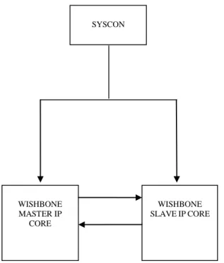
The wishbone bus is system on chip architecture that connects IP cores together and provide portable interface by alleviating integration problem. Wishbone utilizes master and slave architecture and support four interconnections to interface them as point to point, shared bus, crossbar switch and data flow. The wishbone master and slave IP cores are elaborated in section 3. The INTERCON interface master and slave cores. The fig.1 below shows wishbone system.
Fig.1 Wishbone System A. Point to Point Interconnection
The master and slave wishbone IP cores when connected directly represent point to point interconnection. This is the simplest way to connect wishbone cores. The fig. 2 shows point to point interconnection.
Wishbone IP core Generation, Analysis and
Verification for System on Chip Integration
Archana Bharti1, Ayoush Johari2, Soni Changlani3
INTERCON MASTER SLAVE MASTER MASTER SLAVE SLAVE CLOCK RESET
Fig. 2 Point to Point Interconnection
B. Shared Bus Interconnection
The multiple master and slave IP cores when connected on shared basis represent shared bus interconnection. The intercon provides single channel interconnection that is to use bus at a time by multiple masters. The fig. 3 shows shared bus interconnection.
Fig. 3 Shared Bus Interconnection
C. Crossbar Switch Interconnection
The multiple master and slave wishbone IP cores connected but only one master active at a time. The cross bar switch interconnection is more complex than shared bus interconnection. This interconnection has high data transfer rate than shared bus and has arbiter controlling master communication to slave. The fig. 4 shows crossbar switch interconnection containing two masters IP core and three slaves IP cores.
.
Fig. 4 Crossbar Switch Interconnection WISHBONE MASTER IP CORE WISHBONE SLAVE IP CORE WISHBONE MASTER IP CORE WISHBONE MASTER IP CORE WISHBONE SLAVE IP CORE WISHBONE SLAVE IP CORE SYSCON WISHBONE SLAVE IP CORE WISHBONE SLAVE IP CORE WISHBONE SLAVE IP CORE WISHBONE MASTERE IP CORE WISHBONE MASTERE IP CORE
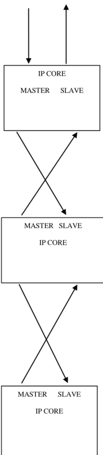
D. Data Flow Interconnection
The master and slave wishbone IP cores when connected in sequential manner allowing IP cores to be master of next IP cores and to be slave to the IP core prior to it. This provide higher data transfer rate as data flow from IP core to IP core in sequential chain and traffic of INTERCON is controlled by handshaking signals. Fig. 5 below shows data flow interconnection.
Fig. 5 Data Flow Interconnection
III. IP CORE GENERATION AND ANALYSIS
IP cores are building blocks and are previously designed component integrated in design for efficient SoC integration. In context to wishbone the IP cores for point to point interconnection are SYSCON, DMA, Memory and INTERCON. The fig. 6 describes point to point interconnection diagram.
The SYSCON generate compatible wishbone clock and reset signal for the system. The external clock signal EXTCLK fed the clock output. According to wishbone reset timing the reset generator produce single RST signal.
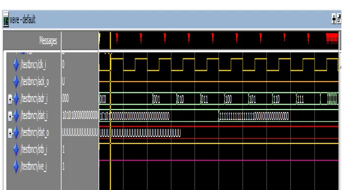
The Memory is 8x32 bit size used as wishbone SLAVE. When input data is given to memory block WE and STB signals are check first. If both signals are asserted then it will write data on memory otherwise data remain unchanged. The memory simulation result is shown in fig. 7.
DMA access the memory block and indicate slave is selected if strobe is asserted but the slave should not take input data when reset is asserted. The input data can be writing on memory block when DMODE, WE and STB signals are asserted. The DMA simulation result is shown in fig. 8
IP CORE MASTER SLAVE MASTER SLAVE IP CORE MASTER SLAVE IP CORE
IV. VERIFICATION RESULT
The verification of proposed system architecture was done using Questasim 6.4c. Simulation result of DMA is shown in fig. 7 and simulation result of memory block is shown in fig. 8.
Fig. 7 DMA Simulation Result
V. CONCLUSION
A 32 bit point to point system is verified in Questasim 6.4c and related issues were discussed. The following conclusion made from above discussion: the DMA and memory signals should properly selected and asserted or negated to get perfect verification result. Hence a low cost portable SoC can be designed successfully by wishbone bus architecture.
ACKNOWLEDGMENT
This paper work is made possible through the help and support from everyone, including: parents, teachers and friends. I would like to deeply thanks my guide, Ayoush Johari an Assistant professor and Soni Changlani an Professor, Department of Electronics and Communication Engineering, LNCTS, Bhopal for guiding and correcting at various stages of my work with attention and care.
REFERENCES
[1] D. Shanthi, R.Amutha, “Design Approach to Implementation of Arbitration Algorithm In Shared Bus Architectures (MPSoC),” IISTE vol 2, No. 4, 2011
[2] Mohandeep Sharma and Dilip Kumar, “Wishbone Bus Architecture-A Survey and Comparison,” International Journal of VLSI Design and Communication System (VLSICS) vol. 3, No. 2, April 2012
[3] Milica Mitic and Mile Stojev, “A Survey of three System On Chip Buses: AMBA, Core Connect and WISHBONE,” ICEST 2006
[4] Bharath S.V., Ashwini S. Shivannavar, and M.Z. Kurian,“Design of Efficient SoC Bus Based on Wishbone,” International Journal of Innovative Technology and Exploring Engineering (IJITEE), ISSN: 2278-3075, vol. 3, Issue 1, June 2013
[5] Chandrala Brijesh A., Mahesh T. Kolte, “Design and Verification Point to Point Architecture of Wishbone Bus for System On Chip,” International Journal of Emerging Engineering Research and Technology, volume. 2, Issue 2, May 2014, pp 155-159
[6] N. Vivekanandan, Abhilash Gunaki, Chinmaya Acharya, Savio Gilbert and Rushikesh Bodake, “Design, Analysis and Simulation of Double Wishbone Suspension System,” IPASI International Journal of Mechnical Engineering (IIJME), volume 2, Issue 6, June 2014
[7] G. Prasad and N. Vasantha, “Integrating a PCI IP Core to FPGA Design and Implementation,” International Journal of Engineering and Advance Technology (IJEAT), ISSN: 2249-8958, Volume 3, Issue 1, October 2013. [8] Richard Herveille, WISHBONE System-on- Chip (SoC) Interconnection Architecture for Portable IP Cores, rev. version: B4, 2010. By Open Cores Organization, p.7, 2010
[9] Simran Rana and Rajesh Mehra, “Design and Simulation of RISC Processor using Hyper Pipeling Technique,” IOSR Journal of Mechnical and Civile Engineering (IOSR-JMCE), e-issn: 2278-1684, P-ISSN:2320-334X, volume 9, Issue 3 (sep-oct 2013), pp 49-57
[10] Ahmed H. M. Soliman, E.M. Saad, M. EI Bably, and Hesham M. A. Keshk, “Designing a Wishbone Protocol Network Adapter for an Asynchronous Network On Chip,” IJCST International Journal of Computer Science Issue, vol. 8, Issue 4, No. 2, July 2011, ISSN (online) : 1694-0814 [11] Ho W.H. and Pinkston T.M., “A Design Methodology for Efficient
Application-specific on-chip interconnects,” IEEE Trans. Parallel Distributed System, 17(2), pp. 174-179, February 2006.
[12] Resve Saleh and Steve Witton, “System On Chip Reuse and Integration,”
Proceedings of the IEEE, vol. 94, NO. 6, pp 1050-1069 June 2006. [13] Gajski, D.D; Wu, A.C-H; Chaiyakul, V.; Mori, S.; Nukiyama, T. and
Bricoud, P., “ Essential Issues for IP Reuse,” Design Automation Conference 2000 Proceedings of the ASP-DAC, Asia and South Pacific pp. 111-114, 2000
[14] Prasun Ghosal, Malabika Biswas, and Manish Biswas, Proceedings of the2010 International Conference on Industrial Engineering and Operation Management Dhaka, Bangladesh, January 9-10, 2010
[15] Ayas Kanta Swain, Kamala Kant Mahapatra, “Design and Verification of Wishbone Bus Interface for System On Chip Integration,” 2010 Annual IEEE India Conference(INDICON)
[16] Kyeong Keol Ryu, Shin, and Vicent J. Mooney, “A Comparison of Five Difference Multi Processor SoC Bus Architectures, “Digital Systems Design,” Proceedings Euro Micro Symposium, Warsaw, Poland, p.209, sept. 2001.
[17] Wishbone System On Chip (SoC) Interconnection Architecture for Portable IP Cores, rev. version: B4, p. 92, 2010
[18] Richard Herveille, “Combining Wishbone Interfaces Signals Application note,” Rev. 0.2 Preliminary, p.2, April 18, 2001, Available Online at http://cdn.Opencores.org/downloads/appnote-01. Pdf
[19] Richard Herveille, “WISHBONE System-on-Chip (SoC) Interconnection Architecture for Portable IP Cores,” Specification Rev. B3, September 7, 2002.
[20] Wishfaq.htm Silicore Corporation p.4, page updated: March 18, 2002.