SH7262/SH7264 Group
Hardware Design Guide
Summary
This application note contains tips on designing a system using the SH7264. As a technical reference it will help the designer avoid common mistakes and get their product up and running when doing their first SH2A design.
Target Device
SH7262/SH7264 MCU (In this document, SH7262/SH7264 are described as "SH7264".)
Contents
1. Power Supplies ... 2
2. Reset ... 7
3. Oscillator Circuit ... 10
4. Operating Mode Control... 12
5. External ROM... 17
6. Handling of Pins ... 21
7. On-chip Resource Access... 26
8. Endianness... 27
9. Power-down Modes... 28
10. References ... 34
Related Application Notes
For more information, refer to the following application notes:
• SH7262/SH7264 Group Guidelines for Hi-Speed USB 2.0 Board Design • SH7262/SH7264 Group Using Deep Standby Mode in Power-down Mode • SH7262/SH7264 Group Connecting the NOR Flash Memory
• SH7262/SH7264 Group Interfacing Serial Flash Memory Using the Renesas Serial Peripheral Interface
About Active-low Pins (Signals)
REJ06B0999-0100 Rev. 1.00 Jun. 30, 2010
1. Power
Supplies
1.1 Power
Supplies
CPU core voltage is between 1.1 V and 1.3 V, and I/O power supply voltage is between 3.0 V and 3.6 V. This LSI (SH7264) uses both digital and analog power supplies. Place the digital circuit and analog circuit as far as possible on the board.
Table 1 lists the digital power supplies. Table 2 lists the analog power supplies. Figure 1 describes the note on using the PLL oscillator circuit.
Table 1 Digital Power Supplies
Symbol Name Voltage Range Description
Vcc Power Supply 1.1 to 1.3 V Power supply pin
Connect all Vcc pins to the system power supply. The system does not work when any of those pins are open.
Vss Ground 0 V Ground pin
Connect all Vss pins to the system power supply (0 V). The system does not work when any of those pins are open.
PVcc I/O circuit power supply 3.0 to 3.6 V Power supply pin for I/O pins. Connect all PVcc pins to the system power supply. The system does not work when any of those pins are open.
USBDPVcc (2) Transceiver digital pin power supply
3.0 to 3.6 V Power supply for USB pins USBDPVss (3) Transceiver digital pin
ground
0 V Ground for USB pins USBDVcc (1) Transceiver digital core
power supply
1.1 to 1.3 V Power supply for USB core USBDVss (3) Transceiver digital core
ground
0 V Ground for USB core USBUVcc (1) Power supply for
480-MHz USB 2.0
host/function modules
1.1 to 1.3 V Power supply for 480-MHz modules
USBUVss (3) Ground for 480-MHz USB 2.0 host/function modules
0 V Ground for 480-MHz modules
Notes: 1. USBAVcc, USBDVcc, and USBUVcc must be at the same electric potential as the Vcc. 2. USBAPVcc and USBDPVcc must be at the same electric potential as the PVcc.
3. USBAVss, USBDVss, USBUVss, USBAPVss, and USBDPVss must be at the same potential as the Vss.
Table 2 Analog Power Supplies
Symbol Name Voltage Range Description
PLLVcc PLL power supply 1.1 to 1.3 V Power supply for internal PLL oscillator PLLVss PLL ground 0 V Ground pin for internal PLL oscillator USBAPVcc (2) (4) Transceiver analog pin
power supply
3.0 to 3.6 V Power supply for USB pins USBAPVss (3) (4) Transceiver analog pin
ground
0 V Ground for USB pins USBAVcc (1) (4) Transceiver analog core
power supply
1.1 to 1.3 V Power supply for USB pins USBAVss (3) (4) Transceiver analog core
ground
0 V Ground for USB core
AVcc (5) (7) Analog power supply 3.0 to 3.6 V A/D Converter power supply pin AVss (5) (7) Analog ground 0 V A/D Converter ground pin
AVref (6) (7) Analog reference voltage 3.0 to 3.6 V A/D Converter reference voltage pin Notes: 1. USBAVcc, USBDVcc, and USBUVcc must be at the same electric potential as the Vcc.
2. USBAPVcc and USBDPVcc must be at the same electric potential as the PVcc.
3. USBAVss, USBDVss, USBUVss, USBAPVss, and USBDPVss must be at the same electric potential as the Vss.
4. Isolate analog power supplies (USBAVcc, USBAVss, USBAPVcc, and USBAPVss) from the digital power supplies.
5. AVcc must be set as PVcc −0.3 V ≤ AVcc ≤ PVcc. AVss must be at the same electric potential as the Vss.
Do not open pins AVcc and AVss when not using the A/D Converter, or in software standby mode. When not using the A/D Converter, connect AVcc to PVcc, and AVss to Vss, respectively.
6. Set the reference voltage range of the AVref pin as 3.0 V ≤ AVref ≤ AVcc.
7. Isolate AVref and AVcc (also A/D Converter analog input pin) from the digital circuit with the AVss. AVss must be connected on a stable digital ground (Vss) on board.
PLLVcc
PLLVss
Vcc
Vss Power supply Signal lines prohibited
Note: When designing the PLLVcc and PLLVss connection pattern for the PLL, signal lines from the board power supply pins must be as short as possible and pattern width must be as wide as possible to reduce inductive interferences. Since the analog power supply pins of the PLL are sensitive to the noise, the system may mulfunction due to inductive interference at the other power supply pins. To prevent such malfunction, do not supply the same resources to the analog power supply pins and the digital power supply pins Vcc and PVcc on the board if at all possible.
1.2 Bypass
Capacitor
A multilayer ceramic capacitor must be installed as a bypass capacitor for each pair of power supply pins. Install the bypass capacitor as close as possible to the LSI power supply pins. Connect the bypass capacitor with capacitance between 0.1 and 0.33 µF (recommended value).
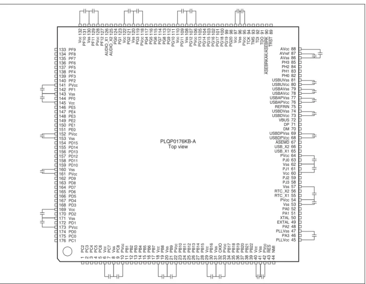
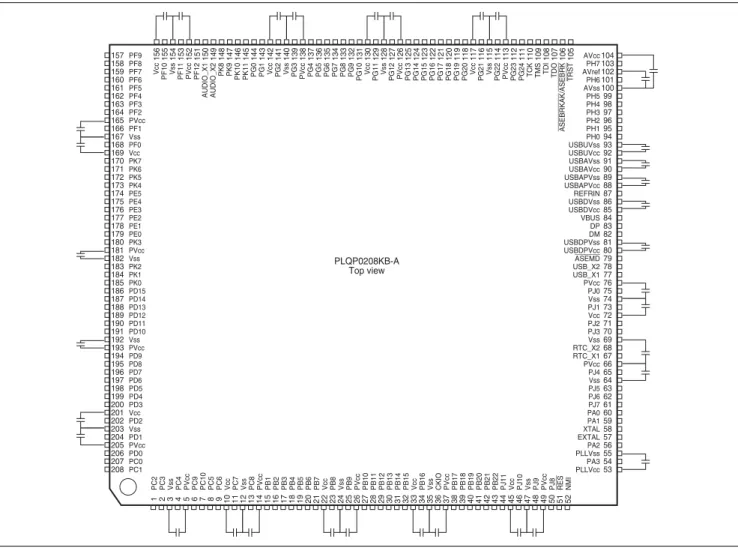
Figure 2 shows an example of installing an external capacitor with the SH7262. Figure 3 shows an example of installing an external capacitor with the SH7264.
133 134 135 136 137 138 139 140 141 142 143 144 145 146 147 148 149 150 151 152 153 154 155 156 157 158 159 160 161 162 163 164 165 166 167 168 169 170 171 172 173 174 175 176 1 2 3 4 5 6 7 8 9 10 11 12 13 14 15 16 17 18 19 20 21 22 23 24 25 26 27 28 29 30 31 32 33 34 35 36 37 38 39 40 41 42 43 44 132 131 130 129 128 127 126 125 124 123 122 121 120 119 118 117 116 115 114 113 112 111 110 109 108 107 106 105 104 103 102 101 100 99 98 97 96 95 94 93 92 91 90 89 88 87 86 85 84 83 82 81 80 79 78 77 76 75 74 73 72 71 70 69 68 67 66 65 64 63 62 61 60 59 58 57 56 55 54 53 52 51 50 49 48 47 46 45 PLQP0176KB-A Top view PF9 PF8 PF7 PF6 PF5 PF4 PF3 PF2 PVcc PF1 Vss PF0 Vcc PE5 PE4 PE3 PE2 PE1 PE0 PVcc Vss PD15 PD14 PD13 PD12 PD11 PD10 Vss PVcc PD9 PD8 PD7 PD6 PD5 PD4 PD3 Vcc PD2 Vss PD1 PVcc PD0 PC0 PC1
PC2 PC3 PC4 PC5 PC6 Vcc PC7 Vss PC8 PVcc PB1 PB2 PB3 PB4 PB5 PB6 PB7 Vcc PB8 Vss PB9 PVcc PB10 PB11 PB12 PB13 PB14 PB15 Vcc PB16 Vss CKIO PVcc PB17 PB18 PB19 PB20 PB21 PB22 Vcc Vss PVcc RES NMI
Vcc PF10 Vss PF11 PVcc PF12 AUDIO_X1 AUDIO_X2 PG0 PG1 Vcc PG2 Vss PG3 PVcc PG4 PG5 PG6 PG7 PG8 PG9 PG10 Vcc PG11 Vss PG12 PVcc PG13 PG14 PG15 PG16 PG17 PG18 PG19 PG20 Vcc Vss PVcc TCK TMS TDI TDO ASEBRKAK / ASEBRK TRST AVcc AVref AVss PH3 PH2 PH1 PH0 USBUVss USBUVcc USBAVss USBAVcc USBAPVss USBAPVcc REFRIN USBDVss USBDVcc VBUS DP DM USBDPVss USBDPVcc ASEMD USB_X2 USB_X1 PVcc PJ0 Vss PJ1 Vcc PJ2 PJ3 Vss RTC_X2 RTC_X1 PVcc Vss PA0 PA1 XTAL EXTAL PA2 PLLVss PA3 PLLVcc
157 158 159 160 161 162 163 164 165 166 167 168 169 170 171 172 173 174 175 176 177 178 179 180 181 182 183 184 185 186 187 188 189 190 191 192 193 194 195 196 197 198 199 200 201 202 203 204 205 206 207 208 1 2 3 4 5 6 7 8 9 10 11 12 13 14 15 16 17 18 19 20 21 22 23 24 25 26 27 28 29 30 31 32 33 34 35 36 37 38 39 40 41 42 43 44 45 46 47 48 49 50 51 52 156 155 154 153 152 151 150 149 148 147 146 145 144 143 142 141 140 139 138 137 136 135 134 133 132 131 130 129 128 127 126 125 124 123 122 121 120 119 118 117 116 115 114 113 112 111 110 109 108 107 106 105 104 103 102 101 100 99 98 97 96 95 94 93 92 91 90 89 88 87 86 85 84 83 82 81 80 79 78 77 76 75 74 73 72 71 70 69 68 67 66 65 64 63 62 61 60 59 58 57 56 55 54 53 PLQP0208KB-A Top view PF9 PF8 PF7 PF6 PF5 PF4 PF3 PF2 PVcc PF1 Vss PF0 Vcc PK7 PK6 PK5 PK4 PE5 PE4 PE3 PE2 PE1 PE0 PK3 PVcc Vss PK2 PK1 PK0 PD15 PD14 PD13 PD12 PD11 PD10 Vss PVcc PD9 PD8 PD7 PD6 PD5 PD4 PD3 Vcc PD2 Vss PD1 PVcc PD0 PC0 PC1
PC2 PC3 Vss PC4 PVcc PC9 PC10 PC5 PC6 Vcc PC7 Vss PC8 PVcc PB1 PB2 PB3 PB4 PB5 PB6 PB7 Vcc PB8 Vss PB9 PVcc PB10 PB11 PB12 PB13 PB14 PB15 Vcc PB16 Vss CKIO PVcc PB17 PB18 PB19 PB20 PB21 PB22 PJ11 Vcc PJ10 Vss PJ9 PVcc PJ8 RES NMI
Vcc PF10 Vss PF11 PVcc PF12 AUDIO_X1 AUDIO_X2 PK8 PK9 PK10 PK11 PG0 PG1 Vcc PG2 Vss PG3 PVcc PG4 PG5 PG6 PG7 PG8 PG9 PG10 Vcc PG11 Vss PG12 PVcc PG13 PG14 PG15 PG16 PG17 PG18 PG19 PG20 Vcc PG21 Vss PG22 PVcc PG23 PG24 TCK TMS TDI TDO ASEBRKAK / ASEBRK TRST AVcc PH7 AVref PH6 AVss PH5 PH4 PH3 PH2 PH1 PH0 USBUVss USBUVcc USBAVss USBAVcc USBAPVss USBAPVcc REFRIN USBDVss USBDVcc VBUS DP DM USBDPVss USBDPVcc ASEMD USB_X2 USB_X1 PVcc PJ0 Vss PJ1 Vcc PJ2 PJ3 Vss RTC_X2 RTC_X1 PVcc PJ4 Vss PJ5 PJ6 PJ7 PA0 PA1 XTAL EXTAL PA2 PLLVss PA3 PLLVcc
2. Reset
2.1 Power-on/Power-off
Sequence
Either the 1.2 V power supplies (Vcc, PLVcc, USBAVcc, USBDVcc, and USBUVcc) or 3.3 V power supplies (PVcc, AVcc, USBAPVcc, and USBDPVcc) can be turned ON or OFF first.
When turning ON the SH7264, make sure to fix pins TRST# and RES# to low level. If not, output pins and I/O pins (output) may be in undefined state to cause malfunction in the entire system.
To avoid such malfunction described above, make sure to fix pins TRST# and RES# to low level when turning OFF the SH7264.
2.2
Oscillation Settling Time
When the RES# pin is driven low, the SH7264 enters the power-on reset state. To make sure to reset the SH7264, the RES# pin must be kept at the low level during the oscillation settling time at power-on, or when exiting from software standby mode and deep standby mode. Keep the RES# pin at low level for at least 20 tcyc when setting the RES# pin to
low level while the clock is running.
The power-on oscillation settling time (tosc1) is 10 ms, which is specified from when the Vcc exceeds the minimum
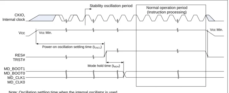
operating voltage until the RES# pin exceeds the VIL voltage. Figure 4 shows the relation between power-on/off and
clock, reset signals. This timing is easily accommodated by many "supervisor" ICs available on the market such as Renesas Electronics RNA51957BFP.
CKIO, Internal clock Vcc RES# TRST# Vcc Min.
Power-on oscillation settling time (tOSC1)
Stability oscillation period
Vcc Min. Normal operation period
(Instruction processing)
Note: Oscillation settling time when the internal oscillator is used. MD_BOOT1
MD_BOOT0 MD_CLK1 MD_CLK0
Mode hold time (tMDH)
2.3 Power-on
Reset
The SH7264 has two reset options; power-on reset and manual reset. This section describes sources for the power-on reset exception handling.
2.3.1 Power-on Reset by the RES# Pin
When the RES# pin is driven low, the SH7264 enters power-on reset state to initialize the CPU’s internal state and all on-chip peripheral registers (note). In power-on reset state, power-on reset exception handling starts when the RES# pin is first driven low for a fixed period and then returns to high. For more information on the "fixed period" to drive the RES# pin low, refer to 2.2 Oscillation Settling Time.
2.3.2 Power-on Reset by the User Debug Interface (H-UDI) Reset Assert Command
When the H-UDI reset assert command is set, the SH7264 enters the power-on reset state to initialize the CPU’s internal state and all on-chip peripheral registers (note), like the power-on reset by the RES# pin. Power-on reset
exception handling starts in power-on reset state. The period required between the H-UDI reset assert command and the H-UDI reset negate command is the same as the period to drive the RES# pin low to start the power-on reset.
2.3.3 Power-on Reset by the Watchdog Timer (WDT)
When setting the WDT as watchdog timer mode, and specifying the power-on reset when the WDT watchdog timer counter (WTCNT) overflows, the SH7264 enters power-on reset state and the WDT starts power-on reset exception handling, however, the Watchdog reset control/status register (WRCSR) of the WDT and the Frequency control register (FRQCR) of the Clock Pulse Generator (CPG) are not initialized (note).
Note: For more information on register status, refer to 36.3 Register States in Each Operating Mode in the SH7262 Group, SH7264 Group Hardware Manual.
2.4 Manual
Reset
This section describes sources for the manual reset exception handling.
2.4.1 Manual Reset by the Watchdog Timer (WDT)
When setting the WDT as watchdog timer mode, and specifying the manual reset when the WTCNT of the WDT overflows, the SH7264 enters manual reset state and the WDT starts manual reset exception handling.
When the SH7264 enters manual reset state while the CPU is leaving the bus or the Direct Memory Access Controller (DMAC) transfers data in burst mode, the manual reset exception handling is deferred until the CPU retrieves the bus. In manual reset state, the SH7264 initializes CPU and the BN bit in the Bank number register (IBNR) of the Interrupt controller (INTC), but FPU and other modules are not included (note).
Note: For more information on register status, refer to 36.3 Register States in Each Operating Mode in the SH7262 Group, SH7264 Group Hardware Manual.
2.5
System Reset by the Watchdog Timer (WDT)
Sometimes it is desirable to have the WDT reset the entire system during an overflow condition using the WDTOVF# signal from the WDT. In this case the WDTOVF# should be not be connected directly to the RES# of the MCU as this would cause problems. A “tiny” gate can be used to OR the “power-on” reset signal and the WDTOVF# as shown in Figure 5: System Reset using WDTOVF#.
RES WDTOVF Reset input (Low active) Reset signal to entire system (Low active)
3. Oscillator
Circuit
3.1 Clock
Pins
Pins listed in the following table can be connected to crystal resonators or input clocks.
Table 3 Clock pins Xin Pin
(Crystal resonator can be connected, or used as external clock input pin)
Xout Pin
(Crystal resonator can be connected)
Remarks
EXTAL XTAL 10 MHz to 18 MHz
USB_X1 USB_X2 • When the USB controller is in high-speed:
48 MHz ± 100 ppm
• When the USB controller is NOT in high-speed and operating as the USB host:
48 MHz ± 500 ppm
• When the USB controller is NOT in high-speed and operating as the USB function:
48 MHz ± 2500 ppm
AUDIO_X1 AUDIO_X2 • When connecting a crystal resonator 10 MHz to 25 MHz
• When inputting an external clock 1 MHz to 25 MHz
RTC_X1 RTC_X2 32.768 kHz
3.2
Connecting an External Clock
Figure 6 shows an example of connecting an external clock to the SH7264. When leaving the Xout pin as open, the parasitic capacitance must be less than 10 pF.
Xin
Xout
SH7264 External clock input
Open
3.3
Connecting a Crystal resonator
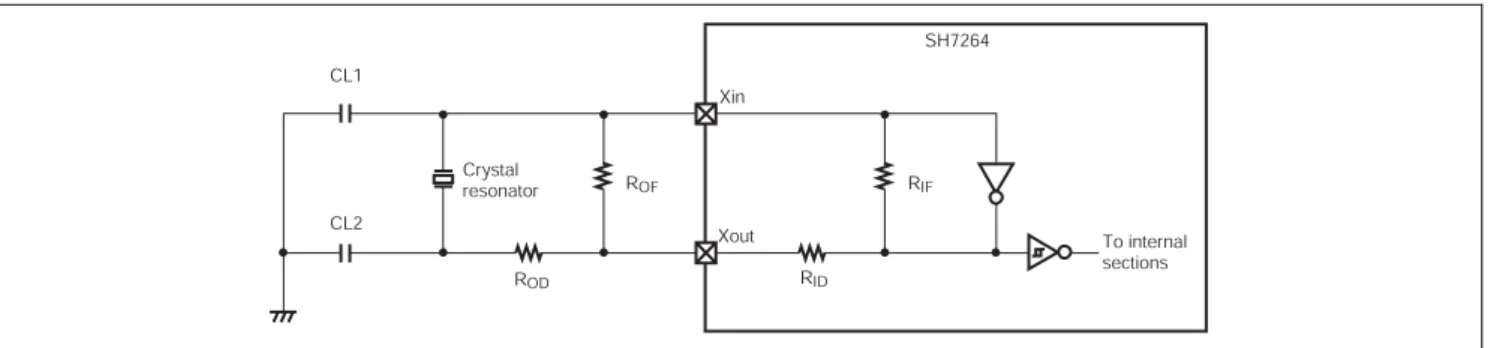
Figure 7 shows an example of connecting a crystal resonator to the SH7264.
Place the crystal resonator and capacitors (CL1 and CL2) as close to pins Xin and Xout as possible. To avoid
inductance and to allow the crystal resonator to oscillate accurately, use the points when the capacitors area connected to the crystal resonator in common and do not place wiring patters close to these components.
Since all the characteristics of the crystal resonator affect the board design, refer to the example shown in Figure 7 and evaluate the entire system before using. As the circuit ratings of the crystal resonator vary with the resonator and the floating capacitance, it is recommended to consult the crystal resonator manufacturer on the constants. Make sure that the applied voltage to the clock pin does not exceed the maximum rating.
The SH7264 includes the feedback resistor, however, an external feedback resistor may be required, according to the characteristics of the crystal resonator. Evaluate the resistor and capacitor thoroughly to set the parameters.
When not using pins Xin and Xout, fix the level on the Xin pin such as pull-up, pull-down, connect to the power supply or ground, and leave the Xout pin as open.
Xin Xout RIF RID ROF ROD SH7264 CL1 CL2 To internal sections Crystal resonator
4. Operating
Mode
Control
The SH7264 has four boot modes and four clock operating modes. These modes can be set by pins MD_BOOT1, MD_BOOT0, MD_CLK1, and MD_CLK0.
4.1 Boot
Modes
4.1.1 Setting the External Pins to Specify Boot Mode
When the RES# pin is driven low, the SH7264 specifies boot mode by external pins. Table 4 lists the relationship between external pins and boot modes.
Table 4 Relationship between External Pins and Boot Modes
MD_BOOT1 MD_BOOT0 Boot Mode
0 0 Boots the MCU from the memory connected to CS0 space (Boot mode 0) 0 1 Boots the MCU from serial flash memory connected to the Renesas Serial
Peripheral Interface channel 0 at high speed (Boot mode 1)
1 0 Boots the MCU from NAND flash memory connected to the NAND flash memory controller (Boot mode 2)
1 1 Boots the MCU from serial flash memory connected to the Renesas Serial Peripheral Interface channel 0 at low speed (Boot mode 3)
4.1.2 Boot Mode 0
Boot mode 0 allows the engineer to boot the SH7264 from memory which is connected to CS0 space. This section describes the steps initiated by the MCU in boot mode 0 (note).
(1) Retrieve the execution start address from the exception handling vector table
After waking up from power-on reset, CPU retrieves the initial values of the program counter (PC) and stack pointer (SP) from the exception handling vector table which is allocated to the CS0 space-connected memory.
(2) Start executing the program
CPU starts executing the program from the PC address retrieved.
NOTE: There is often misunderstanding between booting and execution. Boot Mode 0 actually allows the execution “in place” (i.e. directly from NOR FLASH). The engineer is not required to move code into RAM when in Boot mode 0, nor does it preclude the user from copying and executing the code from RAM (the common notion of booting). NAND and SPI mode are true “boot modes” where the code must be moved from the non-volatile (FLASH) to RAM (internal or external) to be executed.
4.1.3 Boot Modes 1 and 3
Boot modes 1 and 3 allow the engineer to boot the SH7264 from serial flash memory which is connected to channel 0 of the Renesas Serial Peripheral Interface (RSPI). This section describes boot modes 1 and 3. Steps 1 and 2 are initiated by the MCU in SPI boot mode, step 3 (optional) is a function of the “loader” that is being executed (note).
NOTE: This step is listed as optional because the “loader” may not actually perform an application load for various reasons (bad image in FLASH, waiting on Hardware response, waiting on “security” key, etc).
(1) Execute the Internal ROM program to boot
After waking up from power-on reset, CPU executes the program stored in the Internal ROM program to boot (closed).
(2) Transfer the loader program
CPU transfers an 8-KB loader program from the start address of the serial flash memory connected to RSPI channel 0 to the start address of high-speed internal RAM.
In boot mode 1, the communication speed is at the 1/2 of the bus clock (Bφ). In boot mode 3, the communication speed is at the 1/4 of the bus clock (Bφ). Set the boot mode according to the specifications of the serial flash memory used.
After transferring the loader program is completed, CPU jumps to high-speed internal RAM to start executing the transferred loader program.
(3) Transfer the application program (optional)
Use the RSPI within the loader program to load data from serial flash memory to internal RAM or external RAM. Figure 8 shows the schematic view of boot modes 1 and 3.
Internal ROM program to boot (closed)
Loader program (8 KB)
Loader program (8 KB) High-speed internal RAM
Internal RAM
Application program
External RAM Serial flash memory
Application program Application program Renesas serial peripheral interface Channel 0 H'FFF8 0000 H'FFF8 1FFF Read request Read Read Read request SH7264 (1) Execute program
(2) Loading into high-speed internal RAM
(3) Loading into external or internal RAM
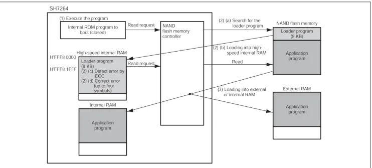
4.1.4 Boot Mode 2
Boot mode 2 allows the engineer to boot the SH7264 from NAND flash memory which is connected to the SH7264 NAND flash memory controller. The SH7264 supports the large-block (2048 bytes + 64 bytes) NAND flash memory with 5-byte address cycles (bigger than 2 Gb density). Number of ECC errors corrected is up to 4. This section describes the steps to initiate boot mode 2. This section describes the steps in boot mode 2. Steps 1 and 2 are initiated by the MCU in NAND boot mode, step 3 (optional) is a function of the “loader” that is being executed (note).
NOTE: This step is listed as optional because the “loader” may not actually perform an application load for various reasons (bad image in FLASH, waiting on Hardware response, waiting on “security” key, etc).
(1) Execute the Internal ROM program to boot
After waking up from power-on reset, CPU executes the program stored in the Internal ROM program to boot (closed).
(2) Transfer the loader program
CPU transfers an 8-KB loader program from the NAND flash memory connected to the NAND flash memory controller to the start address of high-speed internal RAM, as the following steps.
It searches the loader program in NAND flash memory, transfers the loader program to the high-speed internal RAM, and jumps to the entry function of the loader program.
(a) Searches for loader program store blocks (block address 0 to 1023, maximum)
(b) Reads the 8-KB loader program (16 sectors), transfers the loader program to the high-speed internal RAM (c) Detects errors by ECC
(d) Corrects errors (up to four symbols)
After transferring the loader program is completed, CPU jumps to high-speed internal RAM to start executing the transferred loader program.
(3) Transfer the application program (optional)
Use the NAND flash memory controller within the loader program to load data from NAND flash memory to internal RAM or external RAM.
Figure 9 shows the schematic view of boot mode 2.
Internal ROM program to
boot (closed) Loader program
(8 KB)
High-speed internal RAM
Internal RAM
Application program
External RAM NAND flash memory
Application program Application program NAND flash memory controller H'FFF8 0000 H'FFF8 1FFF Read request
(2) (a) Search for the loader program
Read Read request
SH7264
(1) Execute the program
(2) (b) Loading into speed internal RAM
(3) Loading into external or internal RAM Loader program (8 KB) (2) (c) Detect error by ECC (2) (d) Correct error (up to four symbols)
4.2
Clock Operating Modes
4.2.1 External Pins Setting to Decide Clock Operating Modes
When the RES# pin is driven low, the SH7264 uses external pins to decide clock operating modes. Table 5 lists the relationship between external pins and clock operating modes.
Table 5 Relationships between External Pins and Clock Operating Modes
Pin Combination Clock I/O
Mode MD_CLK1 MD_CLK0 Source Output Divider 1 PLL Circuit CKIO Frequency
0 0 0 EXTAL/crystal CKIO 1 ON (×12) (EXTAL/crystal) × 4
1 0 1 USB_X1/crystal CKIO 1/4 ON (×12) (USB_X1/crystal)
2 1 0 EXTAL/crystal CKIO 1 ON (×8) (EXTAL/crystal) × 4
3 1 1 USB_X1/crystal CKIO 1/3 ON (×8) (USB_X1/crystal) × 4/3
4.2.2 Mode 0
Mode 0 provides the clock from the EXTAL pin or a crystal resonator. PLL circuit shapes the waveform and multiplies the frequency to supply the clock to the SH7264. EXTAL pin input clock and crystal resonator within the range of 10 MHz and 12 MHz can be used in mode 0. The CKIO frequency range is 40 MHz to 48 MHz. When the USB 2.0 host or function module is not used, fix the EXTAL pin (connect to pull-up or pull-down resistors, connect to the power supply or ground) and leave the USB_X2 pin open to reduce the power consumption.
4.2.3 Mode 1
Mode 1 provides the clock from the USB_X1 pin or a crystal resonator. PLL circuit shapes the waveform, sets the Frequency control register (FRQCR) to multiply the frequency, and supplies the clock to the SH7264. The CKIO frequency range is (USB_X1/crystal) (48 MHz). To reduce the power consumption, fix the EXTAL pin (connect to pull-up or pull-down resistors, connect to the power supply or ground) and leave the XTAL pin open when using the SH7264 in mode 1.
4.2.4 Mode 2
Mode 2 provides the clock from EXTAL pin or a crystal resonator. PLL circuit shapes the waveform and multiplies the frequency to supply the clock to the SH7264. EXTAL pin input clock and crystal resonator within the range between 10 MHz and 18 MHz can be used in mode 2. The CKIO frequency range is 40 MHz to 72 MHz. When the USB 2.0 host or function module is not used, fix the USB_X1 pin (connect to pull-up or pull-down resistors, connect to the power supply or ground), and leave the USB_X2 pin open to reduce the power consumption.
4.2.5 Mode 3
Mode 3 provides the clock from the USB_X1 pin or a crystal resonator. PLL circuit shapes the waveform, sets the FRQCR to multiply the frequency, and supplies the clock to the SH7264. The CKIO frequency range is
(USB_X1/crystal resonator) × 4/3 (64 MHz). To reduce the power consumption, fix the EXTAL pin (connect to pull-up or pull-down resistors, connect to the power supply or ground), and leave the XTAL pin open when using the SH7264
4.2.6 Available Clock Frequency Range
Table 6 lists clock operating modes and available clock frequency range; do not set these pins other than the combinations shown in the table below.
Table 6 Relationship between Clock Operating Mode and Clock Frequency Range
PLL Multiplier
Available Clock Frequency Range (MHz) Clock Operating Mode FRQCR Setting (1) PLL Circuit Ratio of Internal Clock Frequencies (I:B:P) (2) Input Clock (3) Output Clock (CKIO pin) Internal Clock (Iφ) Bus Clock (Bφ) Peripheral Clock (Pφ) H'x104 ON (×12) 12:4:2 10 to 12 40 to 48 120 to 144 40 to 48 20 to 24 H'x106 ON (×12) 12:4:1 10 to 12 40 to 48 120 to 144 40 to 48 10 to 12 H'x124 ON (×12) 4:4:2 10 to 12 40 to 48 40 to 48 40 to 48 20 to 24 0 H'x126 ON (×12) 4:4:1 10 to 12 40 to 48 40 to 48 40 to 48 10 to 12 H'x104 ON (×12) 3:1:1/2 48 48 144 48 24 H'x106 ON (×12) 3:1:1/4 48 48 144 48 12 H'x124 ON (×12) 1:1:1/2 48 48 48 48 24 1 H'x126 ON (×12) 1:1:1/4 48 48 48 48 12 H'x003 ON (×8) 8:4:2 10 to 18 40 to 72 80 to 144 40 to 72 20 to 36 H'x004 ON (×8) 8:4:4/3 10 to 18 40 to 72 80 to 144 40 to 72 13.3 to 24 H'x005 ON (×8) 8:4:1 10 to 18 40 to 72 80 to 144 40 to 72 10 to 18 H'x006 ON (×8) 8:4:2/3 10 to 18 40 to 72 80 to 144 40 to 72 6.7 to 12 H'x013 ON (×8) 4:4:2 10 to 18 40 to 72 40 to 72 40 to 72 20 to 36 H'x014 ON (×8) 4:4:4/3 10 to 18 40 to 72 40 to 72 40 to 72 13.3 to 24 H'x015 ON (×8) 4:4:1 10 to 18 40 to 72 40 to 72 40 to 72 10 to 18 2 H'x016 ON (×8) 4:4:2/3 10 to 18 40 to 72 40 to 72 40 to 72 6.7 to 12 H'x003 ON (×8) 8/3:4/3:2/3 48 64 128 64 32 H'x004 ON (×8) 8/3:4/3:4/9 48 64 128 64 21.3 H'x005 ON (×8) 8/3:4/3:1/3 48 64 128 64 16 H'x006 ON (×8) 8/3:4/3:2/9 48 64 128 64 10.7 H'x013 ON (×8) 4/3:4/3:2/3 48 64 64 64 32 H'x014 ON (×8) 4/3:4/3:4/9 48 64 64 64 21.3 H'x015 ON (×8) 4/3:4/3:1/3 48 64 64 64 16 3 H'x016 ON (×8) 4/3:4/3:2/9 48 64 64 64 10.7
Notes: 1. "x" in the FRQCR setting depends on the setting in bits 12, 13, and 15.
2. The ratio of clock frequencies, where the input clock frequency is assumed to be 1.
3. These values are the clock frequencies of the EXTAL pin input or a crystal resonator in modes 0 and 2.
In modes 1 and 3, these values are the clock frequencies of the USB_X1 pin input or a crystal resonator.
5. External
ROM
5.1
NOR Flash Memory
Figure 10 shows an example of NOR flash memory circuit.
For more information, refer to the application note "SH7262/SH7264 Group Connecting the NOR Flash Memory".
CE# OE# WE# DQ15 to DQ0 A19 toA0 A20 BYTE# WP#/ACC RY/BY# RESET# VCC VIO
NOR Flash Memory
3.3 V CS0# RD# WE0# D15 to D0 A20 to A1 PB21/A21 MD_BOOT1 MD_BOOT0 RES# VSS SH7264 PVCC VSS 3.3 V 20-bit 16-bit
Note: As damping resistors for signal lines are not indicated, install resistors according to your system configuration.
3.3 V
NC
Reset signal
3.3 V
Figure 10 Typical NOR Flash Memory Circuit
5.1.1 Data Bus Width
On the SH7264 device, CS0 space (area 0) is fixed to 16-bit bus width. The NOR flash memory on CS0 must be connected to operate as 16-bit memory. The NOR flash memory shown in Figure 10 is fixed to 16 bit operation by setting the BYTE# pin to high level.
To boot the SH7264 from NOR flash memory, fix the SH7264 MD_BOOT0 and MD_BOOT1 pins to low level (boot mode 0).
5.1.2 NOR Boot Mode BSC Initial State
In Boot Mode 0 (NOR Boot), the Bus State Controller must be programmed to operate with NOR FLASH. To provide maximum flexibility in the engineers design, the minimal configuration is performed as follows, A1-A20 active, D0-D15 as data bus, RD# and CS0# active. Engineers implementing large NOR FLASH using address lines above A20, must pull these down using resistors to logic 0 to allow code to be fetched from address 0 in the NOR FLASH. An example of this is shown in Figure 10 on A21. Once the user’s code is running they can program the BSC to support the higher address lines as required by their design.
5.2
Serial Flash Memory
Connect the serial flash memory to the SH7264 internal Renesas Peripheral Interface (RSPI). Figure 11 shows an example of serial flash memory circuit. Set the SH7264 pin functions as shown in Table 7.
For more information, refer to the application note "SH7262/SH7264 Group Interfacing Serial Flash Memory Using the Renesas Serial Peripheral Interface".
Serial Flash Memory AT26DF161A
2 MB SH7264
RSPCK0 SCK (Serial Clock)
SI (Serial Data Input) SSL00 WP# (Write Protect) DIP Switches 3.3 V CS# (Chip Select)
SO (Serial Data Output) HOLD# 3.3 V 3.3 V MOSI0 MISO0 3.3 V 3.3 V 3.3 V
Figure 11 Typical Serial Flash Memory Circuit
Note: Pull up or pull down the control signal pins using external resistors.
Pull up or pull down the control signal pins, so the external device does not malfunction when the MCU pins are in the high impedance state. SSL00 pin is pulled up by the external resistor to high level. Pull up or down the RSPCK0 and MOSI0 pins. As the MISO0 pin is an input pin, pull up or down it to avoid floating to an invalid logic level..
Table 7 Multiplexed Pins
SH7264 Port Control Register
Peripheral
Functions Pin Name Register
Name MD Bit Setting
SH7264
Multiplexed Pin Name
RSPI MISO0 PFCR3 PF12MD[2:0] = B'011 PF12/BS#/MISO0/TIOC3D/SPDIF_OUT MOSI0 PFCR2 PF11MD[2:0] = B'011 PF11/A25/SSIDATA3/MOSI0/TIOC3C/SPDIF_IN SSL00 PFCR2 PF10MD[2:0] = B'011 PF10/A24/SSIWS3/SSL00/TIOC3B/FCE# RSPCK0 PFCR2 PF9MD[2:0] = B'011 PF9/A23/SSISCK3/RSPCK0/TIOC3A/FRB Note: SH7264 Multiplexed Pins
MISO0, MOSI0, SSL00, and RSPCK0 pins are multiplexed, and set to general-purpose I/O ports as default. Before accessing serial flash memory, use the general-purpose I/O port control register to set the multiplexed pins to RSPI pins. In SPI Boot mode, these pins are programmed by the loader on power up (refer to SPI boot mode operation).
5.3
NAND Flash Memory
Figure 12 shows an example of NAND flash memory circuit. Set the SH7264 pin functions as shown in Table 8.
K9F2G08U0A 256 MB I/O7 to I/O0 WP# DIP switches CE# NAF7 to NAF0 FCE# FRB
NAND Flash Memory SH7264 3.3 V 3.3 V 3.3 V 8-bit RE# WE# 3.3 V 3.3 V FRE# FWE# R/B# CLE ALE FCLE FALE
Figure 12 Typical NAND Flash Memory Circuit
Note: Pull up or pull down the control signal pins using external resistors.
Pull up or pull down the control signal pins, so the external device does not malfunction when the MCU pins are in the high impedance state. FCE#, FRE#, and FWE# pins are pulled up by the external resistor to high level. FRB pin is also pulled up by an external resistor to high level, as the pin cannot issue commands at low level.
Table 8 Multiplexed Pins
SH7264 Port Control Register
Peripheral
Function Pin Name Register
Name MD Bit Setting
SH7264 Multiplexed Pin Name
NAF4 to NAF7 (1) PDCR3 PD15MD[1:0] = B'01 PD14MD[1:0] = B'01 PD13MD[1:0] = B'01 PD12MD[1:0] = B'01 PD15/D15/NAF7/PWM2H PD14/D14/NAF6/PWM2G PD13/D13/NAF5/PWM2F PD12/D12/NAF4/PWM2E NAF0 to NAF3 (1) PDCR2 PD11MD[1:0] = B'01 PD10MD[1:0] = B'01 PD9MD[1:0] = B'01 PD8MD[1:0] = B'01 PD11/D11/NAF3/PWM2D PD10/D10/NAF2/PWM2C PD9/D9/NAF1/PWM2B PD8/D8/NAF0/PWM2A FWE# (1) PDCR1 PD7MD[1:0] = B'01 PD7/D7/FWE#/PWM1H FALE (1) PDCR1 PD6MD[1:0] = B'01 PD6/D6/FALE/PWM1G FCLE (1) PDCR1 PD5MD[1:0] = B'01 PD5/D5/FCLE/PWM1F FRE# (1) PDCR1 PD4MD[1:0] = B'01 PD4/D4/FRE#/PWM1E FCE# PFCR2 PF10MD[2:0] = B'101 PF10/A24/SSIWS3/SSL00/TIOC3B/FCE# NAND Flash Memory Controller FRB PFCR2 PF9MD[2:0] = B'101 PF9/A23/SSISCK3/RSPCK0/TIOC3A/FRB Note 1: Bus State Controller pin functions (D4 to D15) and NAND Flash Memory Controller pin functions
(NAF0 to NAF7, FWE#, FALE, FCLE, and FRE#) are automatically switched. When using the SH7264 in boot mode 0, D0/NAF0 to D7/NAF7 pin functions are selected as default. When using the SH7264 in boot modes 1 to 3, I/O ports pin functions are selected as default.
6. Handling of Pins
6.1 ASEMD0#
Pin
The ASEMD0# pin selects the H-UDI related functions for use by the emulator.
If the input signal to the ASEMD0# pin is low during the RES# assertion the SH7264 will enter ASE mode. If the input signal is high during the RES# assertion, the MCU will enter product-chip mode (normal operation). Keep the input signal level of the ASEMD0# pin for at least 1 cycle after the RES# pin is negated.
ASEMD0# should have a pull-up resistor so chip enters the correct mode when not being used with the emulator (note). Note: The ASEMD0# pin will be pulled low when using the emulator if the recommended connections as shown in
Figure 13 and Figure 14 are used.
6.2 TRST#
Pin
The TRST# pin is an initialization signal input pin in user debugging interface (UDI). It accepts inputs from the H-UDI serial data I/O clock pin (TCK) asynchronously to reset the H-H-UDI at low level. The TRST# should have a 1K pull-down as shown in Figure 13 and Figure 14 for correct operation whether using or not using the emulator. The emulator will control the TRST# timing when it is being used; in normal mode the engineer does not need to worry about TRST# beyond having the pull-down resistor.
6.3
Signal Wiring to the E10A-USB Connector
Figure 13 and Figure 14 show recommended circuits to wire the H-UDI signal when using the E10A-USB emulator. For more information, refer to the "SuperH™ Family E10A-USB Emulator Additional Document for User’s Manual (Supplementary Information on Using the SH7264 SH7262 SH7266 and SH7267)".
Target MCU 1 AUDATA0 AUDATA2 AUDATA1 AUDATA3 TCK TMS AUDSYNC N.C. N.C. RES TDI TDO TRST ASEBRKAK /ASEBRK UVCC GND GND GND GND (GND) GND GND GND GND GND GND GND GND GND GND GND GND GND GND 3 5 7 9 11 13 15 17 19 21 23 25 27 29 31 33 35 2 4 6 8 12 10 14 16 18 20 22 24 26 28 30 32 34 36 AUDATA0 AUDATA2 AUDATA1 AUDATA3 TCK RES TMS TDO TDI TRST ASEBRKAK/ASEBRK AUDCK AUDSYNC AUDCK N.C. PVcc ASEMD PVcc PVcc 1 kΩ Reset signal
All pins must be pulled up by resistors with 4.7 kΩ or greater.
User system
PVcc = I/O power supply
36-pin H-UDI port connector
1 kΩ
1 TCK TMS RES TDI TDO TRST ASEBRKAK /ASEBRK GND GND GND GND (GND) 2 3 4 5 6 7 ASEMD 8 9 11 10 12 13 14 TCK RES TMS TDO TDI TRST ASEBRKAK/ASEBRK PVcc PVcc N.C. Target MCU PVcc PVcc PVcc UVCC PVcc 1 kΩ Reset signal
All pins must be pulled up by resistors with 4.7 kΩ or greater.
User system
PVcc = I/O power supply
14-pin H-UDI port connector
Figure 14 Recommended Circuit between the 14-pin H-UDI Port Connector and MCU (with E10A-USB)
6.4 Analog
Pins
6.4.1 Notes on Designing Board
Analog pins AN0 to AN7 are input-only, applicable when using as multiplexed PH0 to PH7 ports.
Place the digital circuit and analog circuit as far apart as possible on the board (i.e. maintain some isolation between the high-speed digital and analog signals). Analog circuits signals must be wired prior to digital circuit signals, and avoid intersecting with or being close to the digital circuit signals to avoid coupling. Failure to do so may result in the malfunction of analog circuit and adversely affecting the A/D conversion values.
Isolate analog input signals (AN0 to AN7), analog reference voltage (AVref), analog power supply (AVcc), and analog ground (AVss) from the digital circuit. AVss must be connected on a stable digital ground (Vss) on board.
6.4.2 Analog Pin Protection Circuit
As shown in Figure 15, connect the protection circuit between AVcc and AVss to prevent damage due to an abnormal voltage, such as an excessive surge at analog input pins (AN0 to AN7) and analog reference voltage (AVREF). The circuit also is used as the RC filter to minimize the noise. Note that the circuit shown in the figure below is an example. Consider the circuit constants as appropriate before deciding.
Note: Only analog input pins 0 to 3 (AN0 to AN3) can be used on the SH7262.
SH7264 AVref AVcc AN0 to AN7*3 AVss *1 *1 *2Rin 100 Ω 0.1 μF
Notes: Values are for reference.
2. Rin: Input impedance
3. Only AN0 to AN3 can be used in the SH7262. 0.01 μF
10 μF 1.
Figure 15 Analog Input Pin Protection Circuit Example
6.4.3 Permissible Signal Source Impedance
The SH7264 analog input is designed to guarantee the conversion accuracy for the input signal when its source impedance is equal to or less than 5 kΩ. This specification is to charge the input capacitance of the A/D Converter (ADC) sample-and-hold circuit within the sampling time. When the sensor output impedance exceeds 5 kΩ, charging may be insufficient and it may not be possible to guarantee A/D conversion accuracy. If a large capacitance is provided externally when converting analog to digital in single mode, the input load essentially comprise only the 3kΩ internal input resistance, and the signal source impedance is not required. However, the SH7264 ADC includes a low-pass filter, it may not be able to handle the analog signal with a large differential coefficient (e.g., 5 mV/µs or greater). Install a low-impedance buffer when converting a high-speed analog signal or converting signals in scan mode.
Figure 16 shows an example of the analog input circuit.
Sensor input
SH7264 Sensor output impedance
Low-pass filter C to 0.1 μF Up to 5 kΩ Cin = 15 pF 20 pF 3 kΩ
Note: Values are for reference.
A/D Converter equivalent circuit
6.5 USB
Pins
For details on handling pins to use the USB 2.0 host or function module (USB module), refer to the application note "SH7262/SH7264 Group Guidelines for Hi-Speed USB 2.0 Board Design".
6.6 Terminating
Pins
6.6.1 Unused Pins
Table 9 lists the handling of unused pins.
Table 9 Unused Pins Handling
Pin Name Handling
NMI Fix at high level (pull up or connect to the power supply)
DP, DM, VBUS Connect to the USBDPVss
REFRIN Connect to the USBAPVcc via 5.6 kΩ ± 20% resistor
USB power supply (USBAPVcc, USBAPVss, USBDPVcc, USBDPVss, USBAVcc, USBAVss, USBDVcc, USBDVss, USBUVcc, USBUVss)
Connect to the power supply, ground
AVref Connect to the AVcc
ADC power supply (AVcc, AVss) Connect to the power supply, ground
Other input-only pins Fix the level (pull up, pull down, connect to the power supply or ground)
Other I/O-only pins Set to input pin and fix the level (pull up or pull down) Or set to the output pin and open
Output-only pins Leave open
ASEMD# Fix to high level (pull up or connect to the power supply)
TRST# Fix to low level (pull down or connect to ground)
TCK, TMS, TDI Fix the level (pull up, pull down, connect to the power supply or ground)
TDO, ASEBRKAK#/ASEBRK# Leave open
Note: We recommend using pull-up or pull-down resistors between 4.7 kΩ to 100 kΩ.
6.6.2 Used Pins
The engineer may still need to terminate “used” pins in his design with either pull-up or pull-down resistors. During the RESET cycle GPIO pins will revert to high impedance inputs and remain that way until the hardware setup code is executed, which could be considerable depending on the boot time. The engineer will need to evaluate his design and determine if pull-up or pull-down resistors are required in his design. A prime example would be power circuits, where the engineer will want to passively pull them to the “inactive” state to avoid hardware damage or malfunction.
7. On-chip Resource Access
The SH7264 includes the high-speed internal RAM, large-capacity internal RAM, and on-chip peripheral modules as the on-chip resources. The number of cycles to access the high-speed internal RAM varies according to the bus used. For details on buses connected to on-chip resources, refer to Figure 1.3 Block Diagram in the SH7262 Group, SH7264 Group Hardware Manual.
Table 10 lists the number of cycles for access to the on-chip resources.
Table 10 Number of Cycles for Access to the On-chip Resources
High-speed internal RAM (1)
Internal DMA bus (ID bus)
Read/ Write CPU instruction fetch bus (F bus) CPU memory access bus (M bus) Iφ:Bφ clock ratio Number of cycles to access Large-capacity internal RAM (1) Internal peripheral register 1:1 3 Bφ 2:1 2 Bφ 3:1 2 Bφ 4:1 2 Bφ 6:1 1 Bφ Read 1 Iφ 1 Iφ 8:1 1 Bφ 1 Bφ 2 or more Pφ 1:1 2 Bφ 2:1 2 Bφ 3:1 2 Bφ 4:1 2 Bφ 6:1 1 Bφ Write 1 Iφ 1 Iφ 8:1 1 Bφ 1 Bφ 2 or more Pφ
Note: The High-speed internal RAM and large-capacity internal RAM are composed of several pages, and each page has a port for reading/writing. Periherals may access various RAM pages simultaneously, conflict only occurs when accessing the same page from several buses at the same time, causing some degradation in the RAM performance. This is easily avoided in software by partitioning RAM usage and buffers to avoid that situation (i.e. peripherals accessing the RAM access different pages). A very simple example might be don’t put the stack (high usage memory) in the same memory page where you are capturing video or in a high usage Ethernet buffer and thus avoid “collisions”.
8. Endianness
The SH7264 supports big-endian order to store the most significant byte (MSB) at the lowest address 0, and little-endian order to store the least significant byte (LSB) at the lowest address 0. The default little-endianness is big-little-endian after power-on reset on all areas. The CSn space bus control register (CSnBCR) specifies endian when the target area is not accessed.
Typical memory, SRAM interface with byte selection can be connected in 8- or 16-bit wide, and SDRAM is connected in 16-bit wide (fixed). PCMCIA interface can be connected in 8- or 16-bit wide, and MPX-I/O interface can be connected in 8- or 16-bit wide (fixed), or 8- or 16-bit wide variable, depending on the address to access.
The endianness and data bus width have restrictions per boot mode. NOTE: Since the SH2A is native “big endian”, most common uses of “little-endian” is in data space to connect to “little-endian” devices such as other processors through dual-port memory or “little-endian” memory mapped I/O.
Table 11 lists the boot modes and default state by area.
Note that data position and strobe signals corresponding to addresses depend on the byte order, big-endian or little-endian. WE1 indicates address 0 in big-endian, but WE0 indicates address 0 in little-little-endian.
IMPORTANT: Since the instruction fetch is mixed with the 32- and 16-bit access, code cannot be allocated to the little-endian area. Always execute instructions from the big-little-endian areas, internal or external.
NOTE: Since the SH2A is native “big endian”, most common uses of “little-endian” is in data space to connect to “little-endian” devices such as other processors through dual-port memory or “little-endian” memory mapped I/O.
Table 11 Boot Mode and Default State by Area
Boot Mode Item Area 0 Areas 1 to 6
Data bus width Fixed to 16-bit wide, which cannot be modified
Set to 16-bit by default, which can be modified by program Endianness Fixed to big-endian order, which
cannot be modified
Set to big-endian order by default, which can be modified by program
0
BSC pins setting Minimal pins to read ROM, such as address, data bus, CS0#, and RD# are set automatically. Other pins must be set by program. Data bus width Set to 16-bit by default, which can be modified by program
Endianness Set to big-endian order by default, which can be modified by program 1, 2, 3
BSC pins setting Set to general-purpose port function as default. To access the external bus, all required pins must be set by program.
9. Power-down
Modes
The SH7264 has the following power-down modes and function. (1) Sleep mode
(2) Software standby mode (3) Deep standby mode (4) Module standby function
As power-down modes stop CPU, clock, internal memory, and some peripherals or turns off the power supply, it will reduce power consumption. The SH7264 wakes up from these modes by reset or interrupt.
Table 12 lists transition conditions, module states, and how to wake up the MCU. For more information on the register states, refer to 36.3 Register State in Each Operating Mode in the Sh7262 Group, SH7264 Group Hardware Manual.
Table 12 State of Power-Down Modes
State (1) Power-Down Modes Transition Conditions CPG CPU CPU Register High-speed RAM Cache Memory Large-capacity RAM (Data-retention RAM included) OPM RTC PS External Memory
How to Wake Up the MCU
Sleep mode
Execute SLEEP instruction when the STBY bit in the STBCR1 is 0
ON OFF States held ON ON ON ON (2) ON Auto-refresh • Interrupt
• Manual reset • Power-on reset • DMA address error
Software standby mode
Execute SLEEP instruction when the STBY bit in the STBCR1 is 1 and DEEP bit in the STBCR1 is 0
OFF OFF States held OFF (Data is retained) (5) (6)
OFF (Data is retained) (5) (7)
OFF ON (2) ON Self-refresh • NMI interrupt
• IRQ interrupt • Power-on reset Deep standby mode Execute SLEEP instruction when bits STBY and DEEP in the STBCR1 are 1
OFF OFF OFF OFF (Data is not retained)
OFF (Data in the Data-retention
RAM is retained) (3)
OFF ON (2) OFF Self-refresh • NMI interrupt (4)
• Power-on reset (4)
• Realtime Clock alarm interrupt (4)
• Change pins to wake up the MCU (4)
Module standby mode
Set the MSTP bits in the STBCR2, STBCR3, STBCR4, STBCR5, STBCR6, STBCR7, STBCR8
ON ON States held ON ON Specified
module is OFF
OFF ON Auto-refresh • Clear the MSTP bit to 0 • Power-on reset (Only for
H-UDI and DMAC)
Notes 1. Pin state is either "states held" or "high impedance".
2. The Realtime Clock is ON when the START bit in the RCR2 register is 1. When waking up the MCU from deep standby mode by power-on reset, the operating state cannot be retained. Configure the Realtime Clock again.
3. Set bits RRAMKP3 to RRAMKP0 in the RRAMKP register to 1, and the data stored in the data-retention RAM target area can be retained when the MCU transitions to deep standby mode. Note that the data is initialized when waking up the MCU from deep standby mode by power-on reset. Bits RRAMKP3 and RRAMKP2 can be used only on the MCU with 640-KB RAM.
4. The MCU is woke up from deep standby mode by interrupts (NMI, or real-time clock alarm interrupt), reset (power-on reset), or change pins to wake up the MCU (PC8 to PC5, PG11, PG10, PJ3, and PJ1). When waking up the MCU from deep standby mode not by the reset, the power-on reset exception handling is executed instead of interrupt exception handling. Pins PG11 and PG10 can be used to wake up the MCU only on the MCU with 640-KB RAM.
5. When waking up the MCU from software standby mode by power-on reset, the retained data is initialized.
6. Disable the RAME bit in the SYSCR1 register or RAMWE bit in the SYSCR2 register to retain the data in the high-speed internal RAM when waking up the MCU from software standby mode by power-on reset.
9.1 Sleep
Mode
In sleep mode, only CPU stops its operation.
When executing the SLEEP instruction while the STBY bit in the Standby control register 1 (STBCR1) is 0, the SH7264 transitions from the program execution state to sleep mode. The CPU stops its operation immediately after executing the SLEEP instruction; however internal register values remain unchanged, and on-chip peripherals continue to operate in sleep mode. The CKIO pin continues to output clock pulses.
9.2 Software
Standby
Mode
The SH7264 stops its operation completely in software standby mode.
When executing the SLEEP instruction while the STBY bit in the STBCR1 is 1, and DEEP bit is 0, the SH7264 transitions from the program execution state to software standby mode. Not only the CPU, but the clock and on-chip peripherals stop operation in software standby mode. In addition, the CKIO pin stops outputting clock pulses. CPU and Cache register values are retained in software standby mode. Some on-chip registers are initialized. The CPU writes data in STBCR1 in a cycle and executes the next instruction. However, it takes one or more cycles to actually write data in the register. Therefore, execute the SLEEP instruction after reading STBCR1 to reflect the write value from CPU to STBCR1 in the SLEEP instruction.
9.3
Deep Standby Mode
Deep standby mode stops the SH7264 completely and turns OFF the SH7264.
When executing the SLEEP instruction while the bits STBY and DEEP in STBCR1 is 1, the SH7264 transitions from the program execution state to deep standby mode. Not only the CPU, clock, and on-chip peripheral modules stop operation, but all modules are off, other than the data-retention internal RAM which is set by bits RRAMKP3 to RRAMKP0 in the On-chip data-retention RAM area setting register (RRAMKP) to reduce the power consumption substantially. Therefore, CPU and cache register values, and on-chip peripheral module register values are not retained. Pin states are retained just before transition to deep standby mode.
The CPU writes data in Deep standby cancel source flag register (DSFR) in a cycle and executes the next instruction. However, it takes one or more cycles to actually write data in the register. Therefore, execute the SLEEP instruction after reading the DSFR to reflect the write value from CPU to the DSFR in the SLEEP instruction.
For more information about deep standby mode, refer to the application note "SH7262 Group, SH7264 Group Using Deep Standby Mode in Power-down Mode".
9.4 Module
Standby Function
The module standby function stops on-chip peripherals separately.
Set the MSTP bits in the Standby control registers of each module to 1 to stop supplying clock to the corresponding on-chip peripherals. The power consumption is reduced in power execution state and sleep mode by this function. Make sure to disable a module before setting it in module standby mode. Do not access the registers of a module in module standby mode.
9.5
Pin States in Power-down Modes
9.5.1 Pin States in Sleep Mode
As the peripheral modules operate in sleep mode, the pin state varies according to the operation of peripheral modules.
9.5.2 Pin States in Module Standby Mode
When using module standby function for the module specified as general-purpose I/O port, the pins of the module whose registers to be initialized at the module standby function is configured to default state. The pin of the module whose registers not to be initialized at the module standby function retains the state immediately before entering module standby mode.
9.5.3 Pin States in Software Standby Mode and Deep Standby Mode
The pin states in software standby mode and deep standby mode depend on the pin function or its setting. Table 13 to Table 15 list pin states in software standby mode and deep standby mode.
Table 13 Pin States in Software Standby Mode and Deep Standby Mode (1/3)
Pin Name Description
CKIO Specified by CKOEN [1:0] bits (FRQCR register)
Setting Software standby
mode
Deep standby mode
B'00 Hi-Z Low or high level
B'01 Low level Low or high level B'10 Unstable clock
output
Low or high level
B'11 Hi-Z Hi-Z
A25 to A0, CS6# to CS0#, CE1A#, CE1B#, CE2A#, CE2B#, RD#, RD/WR#, BS#,
ICIOWR#/AH#, ICIORD#, WE1#/DQMLU/WE#, WE0#/DQMLL
Specified by the HIZMEM bit (CMNCR register) 1: Output state
0: High impedance state
RAS#, CAS#, CKE Specified by the HIZCNT bit (CMNCR register) 1: Output state
0: High impedance state External
bus pins
Table 14 Pin States in Software Standby Mode and Deep Standby Mode (2/3)
Pin Name Description
AUDIO_XOUT (only the MCU with 640-KB RAM)
DACK1, DACK0, TEND1, TEND0, TIOC0A to TIOC0D, TIOC1A, TIOC1B, TIOC2A, TIOC2B, TIOC3A to TIOC3D, TIOC4A to TIOC4D,
TxD7 to TxD0, SCK3 to SCK0, RTS1#, CTS1#, RTS3#, CTS3#, MOSI0, MISO0, MISO1, MOSI1, RSPCK1, RSPCK0, SSL10, SSL00, SSITxD0, SSIDATA3 to SSIDATA0, SSISCK3 to SSISCK0, SSIWS3 to SSIWS0, SIOFSCK, SIOFSYNC, SIOFTxD,
CTx1, CTx0, IETxD,
FCE#, FALE, FRE#, FCLE, FWE#, NAF7 to NAF0
LCD_DATA15 to LCD_DATA0, LCD_DE, LCD_CLK, LCD_VSYNC, LCD_HSYNC, LCD_M_DISP, SD_CLK, SD_CMD, SD_D3 to SD_D0, PA3 to PA0, PB22 to PB1, PC10 to PC0, PD15 to PD0, PF12 to PF0, PG24 to PG0, PJ11 to PJ0, PK11 to PK0, PWM1A to PWM1H, PWM2A to PWM2H
Specified by the HIZ bit (STBCR3 register) 1: High impedance state
0: Pin state is retained for output pin and I/O pin which is configured as output pin. Pin state is in high impedance for I/O pin which is configured as input pin
Note: When the AUDIO_XOUT pin state is retained, it outputs either high level or low level signal and does not oscillate.
WDTOVF# High level
XTAL, AUDIO_X2, USB_X2
Low level
Note: When the RCKSEL bit = 1, XTAL is in output state
BACK#,
SCL2 to SCL0, SDA2 to SDA0, PE5 to PE0, PH7 to PH0
High impedance state
DP, DM Software standby mode: Pin state is retained
Deep standby mode: High impedance state Other
output pins, I/O pins
RTC_X2 Specified by the RTCEN bit (RCR2 register)
1: Output state (RTC_X1 is operating) 0: High level (RTC_X1 is operating)
Note: Pins to wake up the MCU from deep standby mode are set to input, regardless of the general-purpose I/O ports setting.
Table 15 Pin States in Software Standby Mode and Deep Standby Mode (3/3)
Pin Name Description
EXTAL Clock operating mode Software standby mode Deep standby mode
0, 2 Input state Hi-Z (Input state when the RCKSEL is 1) 1, 3 Hi-Z AUDIO_CLK, AUDIO_X1, BREQ#, PINT7 to PINT0, DREQ1, DREQ0, TCLKA to TCLKD, AN7 to AN0, ADTRG#, FRB,
USB_X1,
LCD_EXTCLK, DV_CLK, DV_DATA7 to DV_DATA0, DV_VSYNC, DV_HSYNC, SD_CD, SD_WP
High impedance state
RxD7 to RxD0, SSIRxD0, SIOFRxD
High impedance state
RES#, ASEMD#, NMI,
VBUS, REFRIN
Input state
RTC_X1 Specified by the RTCEN bit (RCR2 register)
1: Input state (RTC_X1 is operating)
0: High impedance state (RTC_X1 is stopped) Input pins
IRQ7 to IRQ0, IERxD, CRx1, CRx0
Software standby mode: Input state
Deep standby mode: High impedance state Note: Pins to wake up the MCU from deep standby mode are configured as input, regardless of the
9.5.4 Pin States after Waking Up from Deep Standby Mode
After waking up the MCU from deep standby mode, pin states are retained until the IOKEEP bit in the DSFR register is cleared by 0. However, when the EBUSKEEPE bit is set to 0, external memory control pin states are released
immediately after waking up the MCU from deep standby mode.
Table 16 lists external memory control pins to enable the EBUSKEEPE bit setting.
Table 16 External Memory Control Pins to Enable the EBUSKEEPE Bit Setting
Boot Mode 0 (CS0 Space) Boot Mode 2
(NAND Flash Memory)
Boot Modes 1 and 3 (Serial Flash Memory)
A20 to A1 D15 to D0
CS0#, RD#, CKIO
NAF7 to NAF0 FRE#, FCLE, FALE, FWE#, FCE#, FRB
10. References
• Software Manual
SH-2A, SH2A-FPU Software Manual Rev.3.00
The latest version of the software manual can be downloaded from Renesas Electronics website. • Hardware Manual
SH7262 Group, SH7264 Group Hardware Manual Rev.2.00
The latest version of the hardware manual can be downloaded from Renesas Electronics website. • Emulator Manual
SuperH™ Family E10A-USB Emulator Additional Document for User's Manual (Supplementary Information on Using the SH7264 SH7262 SH7266 and SH7267)
Website and Support
Renesas Technology Website http://www.renesas.com/ Inquiries
Revision Record
Description
Rev. Date Page Summary
General Precautions in the Handling of MPU/MCU Products
The following usage notes are applicable to all MPU/MCU products from Renesas. For detailed usage notes on the products covered by this manual, refer to the relevant sections of the manual. If the descriptions under General Precautions in the Handling of MPU/MCU Products and in the body of the manual differ from each other, the description in the body of the manual takes precedence.
1. Handling of Unused Pins
Handle unused pins in accord with the directions given under Handling of Unused Pins in the manual.
⎯ The input pins of CMOS products are generally in the high-impedance state. In operation with an unused pin in the open-circuit state, extra electromagnetic noise is induced in the vicinity of LSI, an associated shoot-through current flows internally, and malfunctions occur due to the false
recognition of the pin state as an input signal become possible. Unused pins should be handled as described under Handling of Unused Pins in the manual.
2. Processing at Power-on
The state of the product is undefined at the moment when power is supplied.
⎯ The states of internal circuits in the LSI are indeterminate and the states of register settings and pins are undefined at the moment when power is supplied.
In a finished product where the reset signal is applied to the external reset pin, the states of pins are not guaranteed from the moment when power is supplied until the reset process is completed. In a similar way, the states of pins in a product that is reset by an on-chip power-on reset function are not guaranteed from the moment when power is supplied until the power reaches the level at which resetting has been specified.
3. Prohibition of Access to Reserved Addresses Access to reserved addresses is prohibited.
⎯ The reserved addresses are provided for the possible future expansion of functions. Do not access these addresses; the correct operation of LSI is not guaranteed if they are accessed.
4. Clock Signals
After applying a reset, only release the reset line after the operating clock signal has become stable. When switching the clock signal during program execution, wait until the target clock signal has stabilized.
⎯ When the clock signal is generated with an external resonator (or from an external oscillator) during a reset, ensure that the reset line is only released after full stabilization of the clock signal. Moreover, when switching to a clock signal produced with an external resonator (or by an external oscillator) while program execution is in progress, wait until the target clock signal is stable. 5. Differences between Products
Before changing from one product to another, i.e. to one with a different type number, confirm that the change will not lead to problems.
⎯ The characteristics of MPU/MCU in the same group but having different type numbers may differ because of the differences in internal memory capacity and layout pattern. When changing to products of different type numbers, implement a system-evaluation test for each of the products.