Estimation of Reliability of a
Interleaving PFC Boost Converter
Gulam Amer Sandepudi
1, Srinivasa Rao
2Abstract: Reliability plays an important role in power supplies. For other electronic equipment, a certain failure mode, at least for a part of the total system, can often be employed without serious (critical) effects. However, for power supply no such condition can be accepted, since very high demands on its reliability must be achieved. At higher power levels, the continuous conduction mode (CCM) boost converter is preferred topology for implementation a front end with PFC. As a result, significant efforts have been made to improve the performance of high boost converter. This paper is one of the efforts for improving the performance of the converter from the reliability point of view. In this paper, interleaving boost power factor correction converter is simulated with single switch in continuous conduction mode (CCM), discontinuous conduction mode (DCM) and critical conduction mode (CRM) under different output power ratings. Results of the converter are explored from reliability point of view. Keywords: Boost Converter, Reliability, Power factor correction (PFC), Simulation of converter and MIL-HDBK217.
1 Introduction
Reliability is the probability of operating a product for a given period of time without failure under specified conditions and within specified perfor-mance limits. It plays an important role in power electronic systems by which the number of system failures, repair costs, guarantee etc. are estimated [1].
Interleaved converters [2-5] are a result of a parallel connection of switching converters. They usually share the same output filter. Interleaved converters offer several advantages over single-power stage converters; a lower current ripple on the input and output capacitors, faster transient response to load changes and improved power handling capabilities at greater than 90% power efficiency. An interleaved converter can be realized by interleaving the control singles to each of the paralleled converters resulting in an effective increase in its switching frequency. They are used in applications where the loads demand low ripple tolerances. Such requirements are found in the new
1Research Scholar, Department of Electrical Engineering, National Institute of Technology, Warangal, India 2Associate Professor, Dept. of Electrical Engineering, National Institute of Technology, Warangal, AP India
generation of personal computers, in which core voltages and currents of the central processing units are approaching 1V and 130A. Interleaving converters also find applications in switching audio amplifiers by interleaving series or parallel combinations of power inverters. Additionally, interleaving enables the converter to spread its components and the dissipated power over a larger area. Further, interleaving enables the converter to spread its components and the dissipated power over a larger area. Performance comparison of CCM and DCM fly-back converters is referred in [6]. Aspects compared to component stress, output voltage regulation and transient response due to step load and efficiency. The comparison was carried out experimentally on a 5V/25W, 50kHz prototype CCM and DCM fly-back converters which have been designed and built with similar circuit lay outs, components and power ratings. Tests performed on the prototype converter have shown that devices in the CCM fly-back converter sustain the same voltage stress, but lesser current stress than its DCM counterpart, when delivering the same output power. In this comparison, reliability is absent and is not considered, whereas reliability is a key necessity in power electronic devices which the life time, number of failures and associated cost are estimated. In [7, 8] effect of leakage inductance on reduction of reliability of switching power supplies is discussed. In [9], a boost converter is considered as the PFC part of a switching power supply the simulation and reliability calculation of boost converter within DCM and CCM modes operating in three different power ratings is done.
In this paper, a boost power factor correction converter is simulated with single switch interleaving technique in CCM, DCM and CRM modes at different output power ratings and results are compared. Reliability calculation is based on MIL-HDBK217 standard and in part counting method [10]. Results have shown that for an Interleaving boost converter as a PFC, working in CCM mode is better than DCM and CRM mode with reference to reliability.
2 Concept of Reliability
A Reliability
definition
Reliability is a discipline that combines engineering design, manufacture, and test. An efficient reliability program emphasizes early investment in reliability engineering tasks to avoid subsequent cost and schedule delays. The reliability tasks focus on prevention, detection, and correction of design deficiencies, weak pans, and workmanship defects with the goal of influencing the product development process and producing products which operate successfully over the required life [1].
B Reliability
function
The reliability of a component can be described as an exponential function. The probability of finding a component operating after a time period is defined as:
( ) e t
R t = −λ , (1)
where, λ is the constant failure rate during the useful life period. The mathematical mean value of R t( ) occurs at t equal to 1 λ. 1λ is the mean time elapsed until a failure occurs or the ‘‘Mean Time To Failure”, MTTF.
C MTBF (Mean Time between Failures)
As repair time (MTTR) normally can be neglected compared to MTTF for electronics, MTBF can be found as:
MTBF = MTTF + MTTR ≈ MTTF =1λ.
MTBF or the failure rate can be calculated using different kinds of input data.
D Calculation of MTBF for equipment [1]
When calculating the MTBF for equipment, its total failure rate λe must be found. By assuming the equipment or apparatus containing n components.
The probability to find n components in operation after the time t is: 1 2 1 2 e e e n e t t t t n R R R= ⋅⋅⋅⋅⋅⋅⋅⋅⋅R = −λ −λ ⋅⋅⋅⋅⋅⋅⋅⋅ −λ = −λ (2) and 1 2 3 λ = λ + λ + λ + ⋅⋅⋅⋅⋅⋅⋅⋅⋅ + λn. (3)
The total failure rate for the equipment at specified conditions is accordingly achieved as:
1 1 2 2
e bc b c bn nc
λ = λ + λ + ⋅⋅⋅⋅⋅⋅⋅⋅⋅ + λ . (4)
By simply inverting this value, the MTBF figure for the equipment is found: 1 MTBF e = λ . (5)
In this paper, the MOSFET is chosen as IXFH12N100Q/IXS, the Diode MUR850 and the input bridge KBPC_35_06.
3 Interleaved Boost Converter
Interleaved converters offer several advantages over single-power stage converters; a lower current ripple on the input and output capacitors, faster transient response to load changes and improved power handling capabilities at greater than 90% power efficiency. Another important advantage of interleaving is that it effectively increases the switching frequency without increasing the switching losses. The obvious benefit is an increase in the power density without the penalty of reduced power-conversion efficiency. There is still a penalty, however. Interleaving requires increased circuit complexity (greater number of power-handling components and more auxiliary circuitry), leading to higher parts and assembly cost and reduced reliability.
A Continuous conduction mode
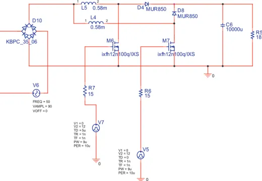
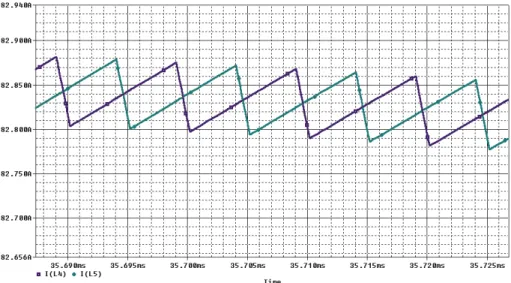
Even though the inductor currents in IL1 and IL2 are discontinuous the input current which is the sum of two inductor currents is continuous [7]. So interleaving virtually eliminates discontinuity in the input current. The simulation of interleaved boost converter is shown in Fig. 1 and inductor current waveform after zooming is shown in Fig. 2.
Fig.2 – Inductor current waveforms after zoom.
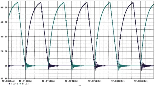
B Discontinuous conduction mode
To operate interleaving configuration in discontinuous mode of operation the phase shift of 180o is properly incorporated between the two inductor
currents by using the delay. The simulation schematic of DCM interleaved converter is shown in Fig. 3 and inductor current waveform is shown in the Fig. 4.
Fig. 4 – Inductor currents waveforms.
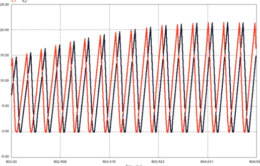
C Critical conduction mode
The interleaved switching converter, composed of parallel connection of switching converters, operating at same switching frequency, but each switching phase is sequentially shifted over equal fractions of the switching period [4]. The simulation schematic of CRM interleaved boost converter is shown in Fig. 5 and inductor current waveform is shown in Fig. 6.
Fig. 6 – Inductor Current waveform.
4 Reliability
Calculations
In this section, reliability of the boost converter for different output power is calculated and presented in detail. For different output powers and operating modes, the results of reliability calculations are shown in Table 1. The part counting method [10] is used to calculate reliability. In this approach, first the failure rate of each element in the converter structure is obtained individually and then the value of the converter’s MTBF is calculated from equations (4) and (5), where “N” is the number of consisting parts. For these calculations the following assumptions are made:
•The ambient temperature is 27oC;
•The control structures of these converters are not the same whose reliability can be neglected for comparing the reliability of main components;
•To calculate the reliability, first the dynamic and static losses of MOSFET and Diodes should be calculated for different output powers working in three operating modes namely CCM, DCM and CRM;
= × × ×
dynamic avg avg ol s
P V I t f , (7)
= × × ×
static on avg on s
P V I t f , (8)
= +
loss static switching
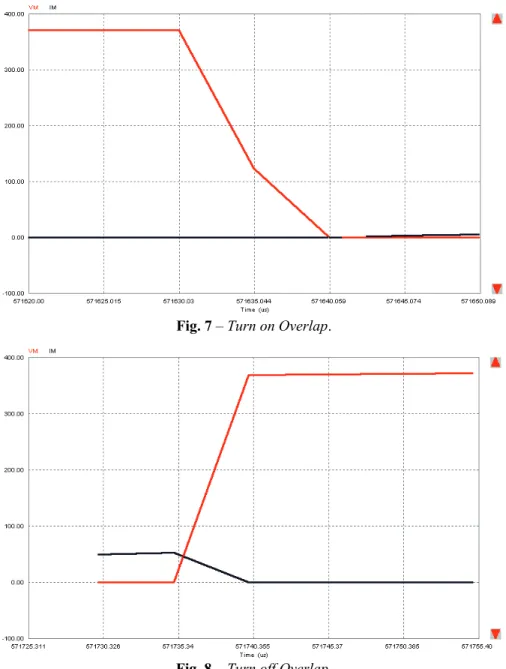
It should be noted that if the converter is operating in DCM mode, then before further turn-on of the switch, the inductor current should reach zero. So there will not be turn-on loss. But in CCM operating mode, the current should be transferred from diode to the switch. The turn ON overlap and turn OFF overlap is shown in Figs. 7 and 8 respectively.
Fig. 7 – Turn on Overlap.
Table 1
Reliability calculations for CCM, DCM and CRM operating modes of interleaving boost PFC.
Output Power 800W 1000W Operating Mode CCM DCM CRM CCM DCM CRM p λ (MOSFET) 76.686 256.9 261.11 90.92 390.41 391.16 p λ (Output Diode) 0.200 2.030 3.145 0.5810 2.776 3.1293 p λ (Input Bridge) 0.103 0.124 0.139 0.1421 0.169 0.181 p λ (Input Inductor) 0.509 0.363 0.362 0.5099 0.362 0.362 p λ (Output Capacitor) 0.060 0.060 0.060 0.0713 0.071 0.071 p λ (Output Resistor) 0.0297 0.0297 0.0297 0.0297 0.0297 0.0297 Total λp 77.59 259.46 264.85 92.25 93.82 394.94 MTBF (hours) 12888 3854 3775 10839 10658 2532
5 Results
From the results noted in the Table-I, the following points are observed. The boost converter has highest reliability in CCM operating mode compared to DCM and CRM modes of operation. The peak and rms values of current are higher in DCM and CRM modes, when compared with CCM, as a result, they offer higher current stress on switching devices. Hence, switching devices have highest failure rate in DCM and CRM modes when compared with CCM mode.
6 Conclusion
In this paper, a boost PFC converter is simulated under three output power ratings and CCM/CRM/DCM operating modes. Reliability calculation of the converter is done based on MIL-HDBK-217 and in part count method. Results have shown that switches have the highest failure rate in the converter structure in both CCM/DCM operating modes and different output powers. It is observed that, with reference to reliability, boost converter as a PFC, working in CCM mode is better when compared with DCM and CRM modes of operation.
7 Appendix
In this section, the sample calculation for failure rate for each component is presented:
a) Calculation of Failure rate λp for MOSFET (IXFH12N100Q/IXS): 1000V n V = , 0.42 C W0 jc θ = , 1 C W0 ca θ =
27 1 69.163875 96.163875 c a ca loss T =T + θ ×P = + × = 96.163875 0.42 69.163875 125.2127 j c jc loss T = + θ ×T P = + × = 1 1 exp 1925 5.08162 273 298 T j T ⎛ ⎛ ⎞⎞ π = ⎜⎜− ×⎜⎜ − ⎟⎟⎟⎟= + ⎝ ⎠ ⎝ ⎠ 0.012, 6, 10 , 5.5 b E A Q λ = π = π = π = 0.012 5.5 6 10 5.08162 20.1232. p b Q E A T λ = λ × π × π × π × π = × × × × =
b) Calculation of failure rate (λp) for Ouput diode: 1000V n V = , 2 C W0 jc θ = , 1 C W0 ca θ = ,Ploss =1.99056W 27 1 1.99056 28.99056 c a ca loss T =T + θ ×P = + × = 27 1 1.99056 32.97168 j c jc loss T = + θ ×T P = + × = 1 1 exp 1925 1.183291 273 298 T j T ⎛ ⎛ ⎞⎞ π = ⎜⎜− ×⎜⎜ − ⎟⎟⎟⎟= + ⎝ ⎠ ⎝ ⎠ 0.069,λ =b π =E 6, π =Q 5.5, π =C 1 2.43 S 90 0.18 0.01549 500 S S V = = ⇒ π =V = p b Q S E T C λ = λ × π × π × π × π × π = 0.069 5.5 0.015 6 1.183291 1 0.041735 = × × × × × = .
c) Calculation of failure rate (λp) for Input Bridge: 1000V n V = , 1.6 C W0 jc θ = ,Ploss =3.8808 W 27 Tc =Ta+ θ ×ca Ploss = + 1 × 3.8808 =30.8808 30.8808 1.6 3.8808 37.09008 j c jc loss T = + θ ×T P = + × = 1 1 exp 1925 1.286413 273 298 T j T ⎛ ⎛ ⎞⎞ π = ⎜⎜− ×⎜⎜ − ⎟⎟⎟⎟= + ⎝ ⎠ ⎝ ⎠
0.069, 6, 5.5, 1 b E Q C λ = π = π = π = 2.43 S 304 0.2533 0.03554 1200 S S V = = ⇒ π =V = λ = λ × π × π × π × π × πp b Q E C S T = 0.069 5.5 6 1 0.03554 1.286413 0.104102 = × × × × × = .
d) Calculation of failure rate (λp) for Inductor:
1.1 27 1.1 11 39.1 HS A T =T + × Δ =T + × = 15.6 273 0.0016 0.70282m 329 HS b T + ⎛ ⎞ λ = ×⎜ ⎟ = ⎝ ⎠ 6, 20 E Q π = π = 3 0.070282 10 6 20 0.08433 p − λ = × × × = .
e) Calculation of failure rate for Capacitor:
(
)
0.18 0.18 0.34 0.34 917 0.09653 CV C ∏ = × = × μ = 2, 10 E Q π = π = 0.13 10 2 0.09653 0.250978. p b Q E CV λ = λ × π × π × π = × × × =f) Calculation of failure rate for Resistor:
1, 2, 10, 0.000066 R E Q b π = π = π = λ = 0.00066 10 2 1 0.0297 p b Q E R λ = λ × π × π × π = × × × =
Therefore the total system failure rate will be:
(
6)
1 20.634 failures / 10 hours N system part n= λ =∑
λ = 1 MTBF 48463.70 ⇒ = = λ .8 References
[1] Reliability aspects on Power Supplies, Design Note 02 EN/LZT 14600 RIA (C. Ericsson
Microelectronics AB).
[2] Simon Ang, Alejdro Olivia: Power Switching Converters, 2nd Edition, Taylor & Francis
2002, page 321 -326.
[3] A. Pressman: Switching Power Supply Design , 2nd edition 1998, McGraw-Hill.
[4] JW Kim, SM Choi and KT Kim: Variable On-time Control of the Critical Conduction Mode
Boost Power Factor Correction Converter to Improve Zero-crossing Distortion, PEDS 2005, Vol 2, pp 1526-1528.
[5] Brett A. Miwa david, M. Otten martin, F. Schlecht: High Efficiency Power Factor
Correction using Interleaving Techniques, APEC 1992, pp 557-568.
[6] S. Howimanporn, C. Unlaksananusorn: Performance comparison of Continuous Conduction
Mode (CCM) and Discontinuous Conduction Mode (DCM) flyback converter”. PEDS, 2003, Vol. 2, pp 1434-1438.
[7] Dao-Shen Chen, Jih-Sheng Lai: A Study of Power Correction Boost Converter Operating at
CCM-DCM Mode”. IEEE Proceedings SOUTH EAST CON '93, 1993.
[8] B. Abdi, M. B. Menhaj, L. Yazdanparast, J. Milimonfared: The Effect of the Transformer
Winding on the Reliability of Switching Power Supplies, EPE-PEMC 2006, pp 663-667.
[9] B. Abdi, A. H. Ranjbar, J Milimonfared, G.B. Gharehpetian: Reliability Comparison of
Boost PFC Converter in DCM and CCM Operating Modes, SPEEDAM 2008, International Symposium on Power Electronics.