Bitmap OSD, Dual HDMI Tx, and Encoder
Data Sheet
ADV8003
Rev. B Document Feedback
Information furnished by Analog Devices is believed to be accurate and reliable. However, no responsibility is assumed by Analog Devices for its use, nor for any infringements of patents or other rights of third parties that may result from its use. Specifications subject to change without notice. No license is granted by implication or otherwise under any patent or patent rights of Analog Devices.
One Technology Way, P.O. Box 9106, Norwood, MA 02062-9106, U.S.A. Tel: 781.329.4700 ©2012–2013 Analog Devices, Inc. All rights reserved.
FEATURES
Video signal processor
Full 12-bit, 4:4:4 YUV internal processing
Motion adaptive de-interlacing with ultralow angle interpolation
Multiple video processing paths
Upscaling to 4k × 2k (ADV8003KBCZ-8x models only) Aspect ratio conversion/panorama scaling
Cadence detection for the recovery of original frames from film-based content
Dual video scalers enable simultaneous output of multiple different resolutions
Sharpness and detail enhancement
Noise reduction to reduce random, mosquito, and block noise
Frame rate converter
Support for up to 3 simultaneous video streams, including picture-in-picture (PiP) support
On-screen display (OSD)
Internally generated bitmap-based OSD allowing overlay on one or more video outputs
Overlay on 3D video formats Dedicated OSD scaler
Alpha blending of OSD data on video data
Disturbance free blending of OSD on either of 2 zones Option of external OSD
Easy to use software tool for developing OSDs
HDMI transmitters
Dual HDMI transmitters enabling splitter capability Content type bits
CEC 1.4 controller
Audio return channel (ARC) support
Support of standard S/PDIF for stereo LPCM compressed audio up to 192 kHz
6-channel uncompressed LPCM I2S audio up to 192 kHz
6-channel direct stream digital (DSD) audio inputs Noise shaped video (NSV) six-DAC video encoder
Six 12-bit NSV video DACs Multiformat video output support
Composite (CVBS), S-Video (Y/C), and Component YPrPb (SD, ED, and HD)
Rovi Rev. 7.1.L1 (SD) and Rev. 1.4 (ED) compliant Simultaneous SD and ED/HD operation
Professional video mode
Capability to output up to 36-bit TTL data
APPLICATIONS
High-end A/V receivers
Upconverting DVD players/recorders Blu-ray players/recorders
Set-top boxes Video conferencing
Standalone video processors HDMI splitters
FUNCTIONAL BLOCK DIAGRAM
24-BIT/ 36-BIT/ 48-BIT VIDEO INPUT 36-BIT VIDEO OUTPUT SERIAL VIDEO RECEIVER AUDIO INPUT DDR2 INTERFACE VIDEO PROCESSING DETAIL ENHANCE LOW ANGLE PROCESSING CADENCE DETECTION MOTION DETECTION CUE CORRECTION DE-INTERLACER NOISE REDUCTION ENHANCE OSD BUILD AND SCALE DUAL SCALER AND OSD BLEND FRC ADV8003 HDMI Tx1 HD VIDEO DACs SD VIDEO DACs HDMI HDMI TTL DATA 60-BIT TTL PORT SERIAL VIDEO FOR EXAMPLE, ADV78500 OUTPUT SD VIDEO HD VIDEO 10556-001 HDMI Tx2 Figure 1.
Comparable Parts
View a parametric search of comparable parts
Evaluation Kits
• ADV8003 Evaluation Board
Documentation
Application Notes
• AN-1249: Converting 3D Images to 2D Images Using the
ADV8003 Evaluation Boards
Data Sheet
• ADV8003: NatureVue™ Video Signal Processor with
Bitmap OSD, Dual HDMI Tx, and Encoder Data Sheet
Software and Systems Requirements
• NatureVue™ OSD Demonstration Software
Reference Materials
Technical Articles
• Solving the Scaling and De-Interlacing Challenges Posed by
Video Systems
Design Resources
• ADV8003 Material Declaration
• PCN-PDN Information
• Quality And Reliability
• Symbols and Footprints
Discussions
View all ADV8003 EngineerZone Discussions
Sample and Buy
Visit the product page to see pricing options
Technical Support
Submit a technical question or find your regional support
number
TABLE OF CONTENTS
Features ... 1
Applications ... 1
Functional Block Diagram ... 1
Revision History ... 2
General Description ... 3
The ADV8003 Family ... 3
Detailed Functional Block Diagram ... 5
Specifications ... 6
Electrical Characteristics ... 6
Analog Specifications ... 7
Data and I
2C Timing Characteristics ... 8
Absolute Maximum Ratings ... 18
ESD Caution ... 18
Pin Configuration and Function Descriptions ... 19
Design Considerations ... 59
Power-Up Sequence ... 59
Thermal Considerations ... 59
Functional Overview... 60
Video Input ... 60
Flexible Digital Core ... 60
Video Signal Processor (VSP) ... 60
On-Screen Display (OSD) ... 61
External DDR2 Memory ... 61
HDMI Transmitters ... 61
Video Encoder ... 61
Professional Configuration ... 61
Register Map Architecture ... 62
Typical Applications Diagram ... 63
Outline Dimensions ... 64
Ordering Guide ... 64
REVISION HISTORY
GENERAL DESCRIPTION
The
ADV8003
is a multiple input video signal processor that can
de-interlace and scale SD, ED, or HD video data to HD formats;
generate a bitmap on-screen display (OSD); and output the video
with OSD overlaid on two High Definition Multimedia Interface
(HDMI®) transmitters and a video encoder.
Video can be input into the
ADV8003
in a number of ways:
using the 48-bit TTL pixel port, using the 24-bit external OSD
TTL pixel port, or from a device with an HDMI transmitter such
as the
ADV7850
. The
ADV8003
supports many of the formats
outlined in the CEA-861 and VESA specifications, as well as
several other widely used timing formats.
Using two external DDR2 memories, the
ADV8003
can perform
high performance, motion adaptive interlaced to progressive
conversion on SD and HD content. Using a single DDR2 memory,
the HD de-interlacing is limited to intrafield.
The
ADV8003
features primary and secondary video scalers
that enable simultaneous output of multiple different resolutions.
The primary video scaler of the ADV8003KBCZ-8/8B/8C models
is capable of upscaling to 4k × 2k format and downscaling from
1080p. The primary video scaler of the ADV8003KBCZ-7/
ADV8003KBCZ-7B/ADV8003KBCZ-7C/ADV8003KBCZ-7T
models is capable of upscaling and downscaling to and from a
1080p format. The secondary video scaler facilitates up-scaling to
1080p and downscaling to 480p. Detail enhancement and image
enhancing techniques such as random, mosquito, and block noise
reduction allow for improved final image quality. The frame rate
converter of the
ADV8003
allows the conversion between
common frame rates with support to output two different frame
rates simultaneously under certain conditions.
VIDEO 48-BIT INPUT 60-BIT INPUT DDR2 INTERFACE DIGITAL CORE HDMI Tx1 HDMI Tx2 1080p (OSD) 1080i (OSD) 480i VIDEO FROM DECODER 720p (OSD) 480i HD VIDEO DACs SD VIDEO DACs 10556-002
Figure 2. Sample Multiple Output Configuration
The
ADV8003
has a flexible digital core that allows the user to
configure the part in several different modes; for example, using
a single video processing channel, using dual video processing
channels, or displaying OSD on multiple outputs of different
resolutions.
The
ADV8003
can accept OSD information from an external OSD
source on the 24-bit external OSD TTL pixel data input or can
internally generate a high quality, bitmap-based OSD. The internal
OSD is highly flexible and allows the system designer to easily
incorporate features like scrolling text and animation in various
color depths up to 24-bit true color.
Analog Devices, Inc., provides an OSD development tool (Blimp)
to assist in the design, debug, and emulation of the OSD prior
to integration with the system application. When the design is
complete, the OSD development tool automatically generates
code to which system APIs can be added before integration with
the system application and an OSD design resource, which must
be downloaded to an external SPI flash memory.
Video can be output from the
ADV8003
using one or both of the
HDMI transmitters and/or the 6-DAC SD/HD video encoder. The
flexible multiplexing allows simultaneous output on the HDMI
transmitters and HD formats on the HD DACs (for example,
1080p) with SD formats on the SD DACs (for example, 480i).
Both of the HDMI transmitters on the ADV8003 support all
mandatory and many optional 3D video resolutions and audio
return channels (ARC). Each transmitter also features a full
CEC master. The
ADV8003
can receive up to six channels of I
2S,
S/PDIF, direct stream digital (DSD), and high bit rate (HBR).
The six 12-bit NSV® video DACs allow for composite (CVBS),
S-Video (Y/C), and component (YPrPb) analog outputs in
standard, enhanced, and high definition video formats.
Over-sampling of 216 MHz (SD and ED) and 297 MHz (HD) removes
the requirement for external output filtering.
The
ADV8003
can also support 30-bit TTL in mode and 30-bit
TTL out mode for professional applications, which do not require
the use of HDMI.
The
ADV8003
supports the I
2C protocol for communication
with the system microcontroller.
THE
ADV8003
FAMILY
There are a number of derivatives
within the
ADV8003
family,
each featuring different capabilities; all are provided in the same
19 mm × 19 mm, 425-ball CSP_BGA package (see Table 1).
Note that the functionality of the ADV8003KBCZ-8 is
described throughout this data sheet. Some sections are not
relevant to other models because not all of the blocks found in
the ADV8003KBCZ-8 are included in those models. Table 1
lists the functionality for each model.
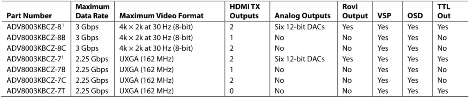
Table 1. Features Sets of the
ADV8003
Family ICs
Part Number Maximum Data Rate Maximum Video Format HDMI TX Outputs Analog Outputs Rovi Output VSP OSD TTL Out
ADV8003KBCZ-81 3 Gbps 4k × 2k at 30 Hz (8-bit) 2 Six 12-bit DACs Yes Yes Yes Yes
ADV8003KBCZ-8B 3 Gbps 4k × 2k at 30 Hz (8-bit) 1 No No Yes Yes No
ADV8003KBCZ-8C 3 Gbps 4k × 2k at 30 Hz (8-bit) 2 No No Yes Yes No
ADV8003KBCZ-71 2.25 Gbps UXGA (162 MHz) 2 Six 12-bit DACs Yes Yes Yes Yes
ADV8003KBCZ-7B 2.25 Gbps UXGA (162 MHz) 1 No No Yes Yes No
ADV8003KBCZ-7C 2.25 Gbps UXGA (162 MHz) 2 No No Yes Yes No
ADV8003KBCZ-7T 2.25 Gbps UXGA (162 MHz) 0 No No Yes Yes Yes
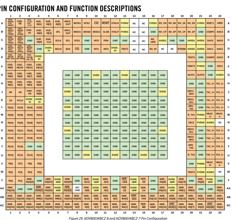
DETAILED FUNCTIONAL BLOCK DIAGRAM
10556-003 O SD VI D EO CAP T URE AND F O RM A TTI N G R EC EI VER CL O CK G EN ER A T ION PO W ER SU PP L Y ARC P O RT I/O, OS D , E N C OD E R VS P , HDM I T x R EG IST ER M A PS SPI SL A VE SPI M A ST ER I 2C S L A VE 2 × PLLs 16 ×/4 × O VERSA MPL IN G F IL TE RS MUL TIPL EXER SYN C IN S E R T ION 12-B IT DAC1 12-B IT DAC2 12-B IT DAC3 12-B IT DAC4 12-B IT DAC5 12-B IT DAC6 S UBCARRI E R F RE Q L O CK V BI D AT A SE R V ICE IN S E R T ION S IN /C OS M O DUL A-T ION /C OS VIDE O M UXING T O P L EVE L CO NT RO L R ESET G EN ER A T ION AND P O W E R M ANAG E M E NT D IGI T A L VI D EO CAP T URE AND F O RM A TTI N G DE -I NT E RL ACE R AND CADE NCE DE T E CT IO N S CAL ING AND F RAM E R A TE CO NV E RS IO N O SD VI D EO BL E ND VI D EO E NHANCE M E NT RANDO M N OIS E RE DUCT IO N M OT ION DE T E CT IO N LO W ANG L E PR O C ESSI N G CADE NCE DE T E CT IO N CUE CO RRE CT IO N M OS QU IT O N OIS E RE DUCT IO N BL O CK N OIS E RE DUCT IO N DE T AI L E NHANCE -M E NT S CAL E R 1 BI T M A P O SD CO NT RO L L E R O SD S CAL E R P RO G RAM M ABL E HDT V F IL T E RS HDM I T x VI D EO D AT A CAP T URE HDC P E NC R YPT IO N HDC P K EYS CE C CO NT RO L HDC P AND E DI D UNCO NT RO L L E R AUDI O D AT A CAP T URE SPI SL A VE T O V B I IN S E R T ION IN E NCO DE R BL O CK I 2C M A ST ER T M DS O UT P UT S HDC P E NC R YPT IO N HDC P K EYS T M DS O UT P UT S RE F E RE NCE AND CABL E DE T E CT IO N 4: 2: 2 4: 4: 4 AND CO L O R S P ACE CO NV E RT E R HDM I T x VI D EO D AT A CAP T URE 4: 2: 2 4: 4: 4 AND CO L O R S P ACE CO NV E RT E R P RO G RAM M ABL E L UM INANCE FI L T E RS P RO G RAM M ABL E CHRO M INANCE FI L T E RS S HARP NE S S AND ADAP T IV E F IL T ER CO NT RO L SD PRO CESSO R ED/ HD PRO CESSO R S CAL E R 2 VI D EO PR O C ESSI N G AND O S D BL E NDI NG DDR2 I NT E R F ACE HE AC CO NT RO L E NCO DE R F RAM E R A TE CO NV E RT E R O SD G EN ER A T ION O S D _I N [15: 13] / V BI _ x O SD _ VS O S D_ DE O S D_ CL K O S D _I N [12] P [35: 0] HS VS DE P CL K RX _ 0 P R X _0N RX _ 1 P R X _1N RX _ 2 P R X _2N RX _ C P RX _ CN RX _ HP D R X _5V X T AL N X T AL P INT 0 INT 1 INT 2 RESET O S D _I N [23: 16] / O S D_ IN[ 1 1: 0] / E X T _D IN [7: 0] PDN SDA SCK1 MISO1 MOSI1 HEAC_1+ HEAC_2– HEAC_2+ ARC1_OUT ARC2_OUT DVDD_IO PVDD_DDR DVDD_DDR AVDDx CVDD1 PVDDx DVDD HEAC_1– CS1 SCK2 MISO2 MOSI2 CS2 SCL ALSB SFL ELPFx VREF COMPx RSETx DAC6 DAC5 DAC4 DAC3 DAC2 DAC1 T X 2_C – T X 2_C + T X 2_2– T X 2_2+ T X 2_1– T X 2_1+ T X 2_0– T X 2_0+ T X 1_C – T X 1_C + T X 1_2– T X 1_2+ T X 1_1– T X 1_1+ T X 1_0– T X 1_0+ HP D_ T X 2 DDC2 _ S D A DDC2 _ S C L DDC1 _ S D A DDC1 _ S C L HP D_ T X 1 CE C2 CE C1 DSD_CLK AUD_IN[5:0] SCLK MCLK DDR_CK DDR_VREF DDR_CK DDR_WE DDR_CS DDR_RAS DDR_A[12:0] DDR_BA[2:0] DDR_DM[3:0] DDR_CAS DDR_DQS[3:0] DDR_DQS[3:0] DDR_DQ[31:0] O S D_ HS COL OR S PACE CONV ERS IO N UPDI THE R COL OR S PACE CONV ERS IO N UPDI THE R COL OR S PACE CONV ERS IO N UPDI THE R DDR2 CO NT RO L L E R I NT E R F ACESPECIFICATIONS
Measured at DVDD = 1.746 V to 1.854 V, DVDD_DDR = 1.746 V to 1.854 V, PVDD1 = 1.746 V to 1.854 V, PVDD2 = 1.746 V to 1.854 V,
PVDD3 = 1.746 V to 1.854 V, PVDD5 = 1.746 V to 1.854 V, PVDD6 = 1.746 V to 1.854 V, PVDD_DDR = 1.746 V to 1.854 V, AVDD3 =
1.746 V to 1.854 V, CVDD1 = 1.746 V to 1.854 V, AVDD1 = 3.20 V to 3.40 V, AVDD2 = 3.20 V to 3.40 V, DVDD_IO = 3.20 V to 3.40 V,
T
MINto T
MAX= 0°C to 70°C, unless otherwise noted.
ELECTRICAL CHARACTERISTICS
Table 2.
Parameter Symbol Test Conditions/Comments Min Typ Max Unit
STATIC PERFORMANCE
Resolution (Each DAC) N 12 Bits
Integral Nonlinearity, +ve1 INL DAC outputs sampled at 500 kHz 0.389 LSB
Integral Nonlinearity, −ve1 INL DAC outputs sampled at 500 kHz −0.322 LSB
Differential Nonlinearity, +ve2 DNL DAC outputs sampled at 500 kHz 0.183 LSB
Differential Nonlinearity, −ve2 DNL DAC outputs sampled at 500 kHz −0.208 LSB
DIGITAL INPUTS
Input High Voltage VIH 0.7 ×
DVDD_IO V
Input Low Voltage VIL 0.3 ×
DVDD_IO V
Input Leakage Current IIN HEAC inputs ±60 µA
DDR_DQS inputs ±60 µA
Other digital inputs ±10 µA
Input Capacitance CIN 13 pF
DIGITAL INPUTS (5 V TOLERANT)
Input High Voltage VIH 3.4 V
Input Low Voltage VIL 0.8 V
Input Leakage Current IIN ±60 µA
DIGITAL OUTPUTS
Output High Voltage VOH 2.4 V
Output Low Voltage VOL 0.4 V
High Impedance Leakage Current ILEAK ±10 µA
Output Capacitance COUT 13 pF
POWER REQUIREMENTS3, 4, 5
Digital Power Supply DVDD 1.746 1.8 1.854 V
PLL Analog Supply PVDD1 1.746 1.8 1.854 V
PLL Digital Supply PVDD2 1.746 1.8 1.854 V
Encoder PLL Supply PVDD3 1.746 1.8 1.854 V
HDMI Tx1 PLL Power Supply PVDD5 1.746 1.8 1.854 V
HDMI Tx2 PLL Power Supply PVDD6 1.746 1.8 1.854 V
HDMI Analog Power Supply AVDD3 1.746 1.8 1.854 V
Comparator Power Supply CVDD1 1.746 1.8 1.854 V
HDMI Rx Inputs Analog Supply AVDD1 3.20 3.3 3.40 V
Encoder Analog Power Supply AVDD2 3.20 3.3 3.40 V
Digital Interface Supply DVDD_IO 3.20 3.3 3.40 V
Digital Power Supply Current, Including DVDD_DDR and PVDD_DDR
IDVDD Mode 1 1989.0 mA
Mode 2 1423.0 mA
Power-down mode 60.6 mA
PLL Analog Supply Current IPVDD1 Mode 1 23.0 mA
Mode 2 21.0 mA
Power-down mode 1.3 mA
PLL Digital Supply Current IPVDD2 Mode 1 21.8 mA
Mode 2 19.9 mA
Parameter Symbol Test Conditions/Comments Min Typ Max Unit
Encoder PLL Supply Current IPVDD3 Mode 1 8.9 mA
Mode 2 3.8 mA
Power-down mode 0.0 mA
HDMI Tx1 PLL Supply Current IPVDD5 Mode 1 62.2 mA
Mode 2 49.3 mA
Power-down mode 1.8 mA
HDMI Tx2 PLL Supply Current IPVDD6 Mode 1 62.5 mA
Mode 2 2.1 mA
Power-down mode 1.6 mA
HDMI Analog Power Supply Current IAVDD3 Mode 1 52.9 mA
Mode 2 19.7 mA
Power-down mode 3.6 mA
Comparator Power Supply Current ICVDD1 Mode 1 76.1 mA
Mode 2 69.6 mA
Power-down mode 1.1 mA
HDMI Rx Inputs Analog Supply Current IAVDD1 Mode 1 62.3 mA
Mode 2 56.8 mA
Power-down mode 6.3 mA
Encoder Analog Power Supply IAVDD2 Mode 1 36.2 mA
Mode 2 9.2 mA
Power-down mode 1.9 mA
Digital Interface Supply Current IDVDD_IO Mode 1 1.14 mA
Mode 2 1.93 mA
Power-down mode 0.1 mA
1 Integral nonlinearity (INL) measures the deviation of the actual DAC transfer function from the ideal. For +ve INL, the actual line lies above the ideal line value. For −ve INL, the actual line lies below the ideal line value.
2 Differential nonlinearity (DNL) measures the deviation of the actual DAC output voltage step from the ideal. For +ve DNL, the actual step value lies above the ideal step value. For −ve DNL, the actual step value lies below the ideal step value.
3 Mode 1 involves a 1080i60 input to the ADV8003 receiver and a 720p60 input to the ADV8003 TTL external OSD input. Both inputs are run through the front-end color space converters. The 1080i60 video stream is de-interlaced and upscaled to 4k × 2k at 24 Hz. The 720p video stream is input to the OSD block and is blended onto the 4k × 2k at 24 Hz video stream using the OSD block scaler. Both HDMI transmitters are then driven using the 4k × 2k at 24 Hz output.
4 Mode 2 involves a 1080i60 input to the ADV8003 receiver. This input is run through the front-end color space converter. The 1080i60 video stream is de-interlaced and is output to HDMI Transmitter 1. The secondary VSP is used to convert the 1080p video stream to 480i and is output using the SD encoder.
5 In the power-down mode, the ARC and the internal clock tree are kept active.
ANALOG SPECIFICATIONS
Table 3.
Parameter Test Conditions/Comments Min Typ Max Unit
Low Drive Output Current (Full Scale) RSET = 4.12 kΩ, RL = 300 Ω 3.95 4.3 4.5 mA
DAC-to-DAC Matching DAC1 to DAC6 0.9 %
Output Compliance, VOC 0 1.4 V
Output Capacitance, COUT DAC1, DAC2, DAC3 9 pF
DAC4, DAC5, DAC6 9 pF
DATA AND I
2C TIMING CHARACTERISTICS
For input timing measurements, V
IH= DVDD_IO and V
IL= GND.
Table 4.
Parameter Symbol Test Conditions/Comments Min Typ Max Unit
TMDS CLOCK
TMDS Input Clock Frequency ADV8003KBCZ-8,
ADV8003KBCZ-8B, ADV8003KBCZ-8C 25 297 MHz ADV8003KBCZ-7, ADV8003KBCZ-7B, ADV8003KBCZ-7C, ADV8003KBCZ-7T 25 225 MHz
TMDS Output Clock Frequency ADV8003KBCZ-8,
ADV8003KBCZ-8B, ADV8003KBCZ-8C 25 297 MHz ADV8003KBCZ-7, ADV8003KBCZ-7B, ADV8003KBCZ-7C, ADV8003KBCZ-7T 25 225 MHz
CLOCK AND CRYSTAL
Crystal Frequency, XTAL 27 MHz
Crystal Frequency Stability ±50 ppm
Primary Video Input Clock Frequency Range 13.5 162 MHz
Secondary Video Input Clock Frequency Range 13.5 162 MHz
Video Output Clock Frequency Range 13.5 162 MHz
Serial Port 1 SCK Frequency (SCK1) 50 MHz
Serial Port 2 SCK Frequency (SCK2) 11.5 81 MHz
Serial Port 3 SCK Frequency (VBI_SCK) 27 MHz
Audio SCLK Frequency 49.152 MHz
Audio MCLK Frequency 98.304 MHz
Audio DSD Clock Frequency 5.6448 MHz
FAST I2C PORTS1
SCL Frequency 400 kHz
SCL Minimum Pulse Width High t1 600 ns
SCL Minimum Pulse Width Low t2 1.3 µs
Start Condition Hold Time t3 600 ns
Start Condition Setup Time t4 600 ns
SDA Setup Time t5 100 ns
SCL and SDA Rise Time t6 300 ns
SCL and SDA Fall Time t7 300 ns
Stop Condition Setup Time t8 0.6 µs
SERIAL PORT2, 3
Master Serial Port (Serial Port 2)
CS2 Falling Edge to SCK2 Rising/Falling Edge t9, t10 t9, t10, depending on the
values of CPHA and CPOL 1 × SCK2 periods 1.5 × SCLK2 periods ns
SCK2 Rising/Falling Edge to CS2 Rising Edge t11, t12 t11, t12, depending on the
values of CPHA and CPOL
1 × SCK2 periods 1.5 × SCLK2 periods ns CS2 Pulse Width t13 1880 1900 ns SCK2 High Time t14 0.45 × SCLK2 periods 0.55 × SCLK2 periods % duty cycle SCK2 Low Time 0.45 × SCLK2 periods 0.55 × SCLK2 periods % duty cycle
Parameter Symbol Test Conditions/Comments Min Typ Max Unit
MOSI2 Start of Data Invalid to SCK2 Falling Edge t15 SPI Mode 0, SPI Mode 3 1.15 ns
CS2 Start of Data Invalid to SCK2 Falling Edge
t15 SPI Mode 0, SPI Mode 3 0.81 ns
SCK2 Falling Edge to MOSI2 End of Data Invalid t16 SPI Mode 0, SPI Mode 3 1.85 ns
SCK2 Falling Edge to CS2 End of Data Invalid t16 SPI Mode 0, SPI Mode 3 2.14 ns
MISO2 Setup Time t17 Valid regardless of the
SCK2 active edge used
14.57 ns
MISO2 Hold Time t18 Valid regardless of the
SCK2 active edge used 0.0 ns
MOSI2 Start of Data Invalid to SCK2 Rising Edge t19 SPI Mode 1, SPI Mode 2 1.59 ns
CS2 Start of Data Invalid to SCK2 Rising Edge t19 SPI Mode 1, SPI Mode 2 1.24 ns
SCK2 Rising Edge to MOSI2 End of Data Invalid t20 SPI Mode 1, SPI Mode 2 1.39 ns
SCK2 Rising Edge to CS2 End of Data Invalid t20 SPI Mode 1, SPI Mode 2 1.68 ns
MISO2 Setup Time t21 Valid regardless of the
SCK2 active edge used
14.57 ns
MISO2 Hold Time t22 Valid regardless of the
SCK2 active edge used 0.0 ns
Slave Mode (Serial Port 1)
CS1 Falling Edge to SCK1 Rising/Falling Edge t23, t24 t23, t24, depending on the
values of CPHA and CPOL 50.0 ns
SCK1 Rising/Falling Edge to CS1 Rising Edge t25, t26 t25, t26, depending on the
values of CPHA and CPOL 50.0 ns
CS1 Pulse Width t27 5 × SCK1 periods ns SCK1 High Time t30 0.45 × SCK1 periods 0.55 × SCK1 periods % duty cycle SCK1 Low Time 0.45 × SCK1
periods 0.55 × SCK1 periods % duty
cycle
MOSI1 Setup Time t31 SPI Mode 0, SPI Mode 3 0.15 ns
MOSI1 Hold Time t32 SPI Mode 0, SPI Mode 3 1.4 ns
SCK1 Falling Edge to MISO1 Start of Data Invalid
t33 SPI Mode 0, SPI Mode 3 5.89 ns
SCK1 Falling Edge to MISO1 End of Data Invalid t34 SPI Mode 0, SPI Mode 3 12.08 ns
MOSI1 Setup Time t35 SPI Mode 1, SPI Mode 2 0 ns
MOSI1 Hold Time t36 SPI Mode 1, SPI Mode 2 1.96 ns
SCK1 Rising Edge to MISO1 Start of Data Invalid t37 SPI Mode 1, SPI Mode 2 5.79 ns
SCK1 Rising Edge to MISO1 End of Data Invalid t38 SPI Mode 1, SPI Mode 2 11.97 ns
Slave Mode (Serial Port 3)
VBI_SCK High Time t39 0.45 ×
VBI_SCK periods 0.55 × VBI_SCK periods % duty cycle
VBI_SCK Low Time 0.45 ×
VBI_SCK periods 0.55 × VBI_SCK periods % duty cycle
VBI_CS Pulse Width 5 ×
VBI_SCK periods
ns
VBI_CS, VBI_MOSI Setup Time t40 SPI Mode 0 only 0.93 ns
Parameter Symbol Test Conditions/Comments Min Typ Max Unit
SPI Pass-Through Mode
Data Transition on SCK1 to Start of Data Invalid on SCK2
t42 5.17 ns
Data Transition on SCK1 to End of Data Invalid
on SCK2 t
43 10.20 ns
Data Transition on MOSI1 to Start of Data
Invalid on MOSI2 t
42 4.90 ns
Data Transition on MOSI1 to End of Data Invalid
on MOSI2 t
43 10.85 ns
Data Transition on MISO2 to Start of Data Invalid on MISO1
t42 5.29 ns
Data Transition on MISO2 to End of Data Invalid
on MISO1 t
43 11.97 ns
Data Transition on CS1 to Start of Data
Invalid on CS2
t42 4.61 ns
Data Transition on CS1 to End of Data Invalid
on CS2
t43 8.78 ns
RESET FUNCTION
Reset Pulse Width 5 ms
VIDEO DATA AND CONTROL INPUTS3
PCLK High Time t44 0.45 × PCLK
period 0.55 × PCLK period % duty
cycle PCLK Low Time 0.45 × PCLK period 0.55 × PCLK period % duty cycle
OSD_CLK High Time t51 0.45 ×
OSD_CLK period 0.55 × OSD_CLK period % duty cycle
OSD_CLK Low Time 0.45 ×
OSD_CLK period 0.55 × OSD_CLK period % duty cycle Main Video Input, SDR and DDR Mode Setup
Time (Data Latched on Rising Edge) t
45 1.42 ns
Main Video Input, SDR and DDR Modes Hold Time (Data Latched on Rising Edge)
t46 0.95 ns
Main Video Input, DDR Mode Setup Time
(Data Latched on Falling Edge) t
47 0.72 ns
Main Video Input, DDR Mode Hold Time
(Data Latched on Falling Edge) t
48 1.49 ns
Interleaved Video Input, SDR Setup Time
(Data Latched on Rising Edge) t
49 Used for 300 MHz TTL data 1.42 ns
Interleaved Video Input, SDR Hold Time
(Data Latched on Rising Edge) t
50 Used for 300 MHz TTL data 0.95 ns
External OSD Input, SDR and DDR Mode Setup Time (Data Latched on Rising Edge)
t52 1.33 ns
External OSD Input, SDR and DDR Mode Hold
Time (Data Latched on Rising Edge) t
53 0.94 ns
External OSD Input, DDR Mode Setup Time
(Data Latched on Rising Edge) t54 0.57 ns
External OSD Input, DDR Mode Hold Time
(Data Latched on Rising Edge) t
Parameter Symbol Test Conditions/Comments Min Typ Max Unit
VIDEO DATA AND CONTROL OUTPUTS3
OSD_CLK High Time t56 0.40 ×
OSD_CLK period 0.60 × OSD_CLK period % duty cycle
OSD_CLK Low Time 0.40 ×
OSD_CLK period 0.60 × OSD_CLK period % duty cycle OSD_CLK Active Edge to Data and Control
Start of Data Invalid (Data Latched on Falling Edge)
t57 0.07 ns
OSD_CLK Active Edge to Data and Control End
of Data Invalid (Data Latched on Falling Edge) t
58 1.56 ns
OSD_CLK Active Edge to Data and Control Start of Data Invalid (Data Latched on Rising Edge)
t59 0.41 ns
OSD_CLK Active Edge to Data and Control End
of Data Invalid (Data Latched on Rising Edge) t
60 0.93 ns S/PDIF INPUT3 MCLK High Time t61 0.45 × MCLK periods 0.55 × MCLK periods % duty cycle MCLK Low Time 0.45 × MCLK periods 0.55 × MCLK periods % duty cycle
S/PDIF Data Setup Time t62 0.12 ns
S/PDIF Data Hold Time t63 1.89 ns
I2S PORT, SLAVE MODE3
SCLK High Time t64 0.45 × SCLK periods 0.55 × SCLK periods % duty cycle SCLK Low Time 0.45 × SCLK periods 0.55 × SCLK periods % duty cycle
I2S Data Setup Time t65 0.42 ns
I2S Data Hold Time t66 1.38 ns
DSD PORT3
DSD Clock High Time t67 0.45 × DSD
CLK periods 0.55 × DSDCLK
periods % duty cycle
DSD Clock Low Time 0.45 × SCLK
periods 0.55 × SCLK periods % duty
cycle
DSD Data Setup Time t68 0.48 ns
DSD Data Hold Time t69 1.79 ns
1 It is possible to run I2C at faster speeds; however, it has been characterized to run only in fast mode.
2 All serial port measurements are for the default polarity and phase settings (clock low in idle state and negative edge used). 3 All measurements are guaranteed by design only.
Timing Diagrams
SDA SCL t5 t3 t6 t1 t3 004
10556-005
23 22 21 ... 3 2 1 0 7 6 5 4 3 2 1 0
INSTRUCTION(0x0B) 24-BIT ADDRESS DUMMY BYTE
7 6 5 4 3 2 1 0
MOSI2
MISO2 7 6 5 4 3 2 1 0
DATA OUT 1 DATA OUT 2
CPOL CPHA 0 0 0 1 1 0 1 1 SPI MODE 0 1 2 3 SCK2 SCK2 SCK2 SCK2 CS2 t9 t10 t11 t12 t13
Figure 5. Detailed SPI Master Timing Diagram (Serial Port 2)
10556-006 SCK2 MOSI2 CS2 MISO2 (FALLING EDGE CAPTURE) MISO2 (RISING EDGE CAPTURE)
t14 t17
t15
t16
t18 t18
t17
Figure 6. Serial Port 2 Master Mode Timing (SPI Mode 0 and SPI Mode 3)
SCK2
MOSI2 CS2
MISO2 (FALLING EDGE CAPTURE) MISO2 (RISING EDGE CAPTURE)
t14 t19 t20 t21 t22 t21 t22 10556-007
SCK1 SCK1 SCK1 SCK1 CS1 MOSI1 DELAY MODE 0 MISO1 DELAY MODE 1 MISO1
DEVICE ADDRESS SUB ADDRESS DATA IN 0 DATA IN 1
DUMMY BYTE DATA OUT 0
DATA OUT 0 DATA OUT 1 W/R 7 6 5 4 3 2 1 0 7 6 5 4 3 2 1 0 7 6 5 4 3 2 1 0 7 6 5 4 3 2 1 0 7 6 5 4 3 2 1 0 7 6 5 4 3 2 1 0 7 6 5 4 3 2 1 0 t25 t27 t26 t23 t24 10556-008 CPOL CPHA 0 0 0 1 1 0 1 1 SPI MODE 0 1 2 3
Figure 8. Detailed SPI Slave Timing Diagram (Serial Port 1)
10556-009 SCK1 MOSI1 MISO1 t30 t31 t32 t33 t34
Figure 9. Serial Port 1 Slave Mode Timing (SPI Mode 0 and SPI Mode 3)
10556-010 SCK1 MOSI1 MISO1 t30 t35 t36 t37 t38
Figure 10. Serial Port 1 Slave Mode Timing (SPI Mode 1 and SPI Mode 2)
10556-0 1 1 VBI_SCK VBI_MOSI VBI_CS t39 t40 t41
10556-012 SCK1 MISO2 MOSI1 CS1 t42 t43 SCK2 MISO1 MOSI2 CS2
Figure 12. SPI Pass-Through Mode (Serial Port 1 and Serial Port 2)
t44 t45 t46 PCLK P[35:0] HS VS DE 10556-013
Figure 13. Main Video Input, Noninterleaved SDR Video Data and Control Timing
10556-014 t48 t47 t46 t45 PCLK P[35:0] HS VS DE t44
Figure 14. Main Video Input, Noninterleaved DDR Video Data and Control Timing
t50 t49 PCLK OSD_IN[11:0] P[23:0] HS VS DE P[35:24] t44 10556-015
t51 t53 t52 OSD_CLK OSD_IN[23:0] OSD_HS OSD_VS OSD_DE 10556-016
Figure 16. External OSD Input, Noninterleaved SDR Video Data and Control Timing
10556-017 t55 t54 t53 t52 OSD_CLK OSD_IN[23:0] OSD_HS OSD_VS OSD_DE t51
Figure 17. External OSD Input, Noninterleaved DDR Video Data and Control Timing
OSD_CLK OSD_IN[23:0] OSD_HS OSD_VS OSD_DE P[35:24] t56 t57 t58 10556-018
Figure 18. SDR Video Data and Control Output Timing (Data Launched on Falling Edge)
OSD_CLK OSD_IN[23:0] OSD_HS OSD_VS OSD_DE P[35:24] t56 t59 t60 10556-1 19
t61 t63 t62 MCLK S/PDIF AUDIO DATA 10556-120
Figure 20. S/PDIF Input Timing, Data Latched on Rising Edge
S/PDIF
SYNC IMPULSE DATA
1.5 ×tMCLK
0.5 ×tMCLK
tMCLK
10556-020
Figure 21. S/PDIF Data Timing
t64 t66 t65 SCLK I2S[3:0] LRCLK 10556-021 Figure 22. I2S Timing AUD_IN[5] SCLK
AUD_IN[4:1] MSBLEFT LSB MSBRIGHT LSB
LEFT RIGHT
I2S STANDARD I2S FORMAT = 00
32 CLOCK SLOTS 32 CLOCK SLOTS
10556-022
Figure 23. I2S Standard Audio—Data Width of 16 Bits to 24 Bits per Channel
AUD_IN[5]
SCLK
AUD_IN[4:1] LSB
LEFT RIGHT
I2S STANDARD 16-BIT PER CHANNEL I2S FORMAT = 00
16 CLOCK SLOTS 16 CLOCK SLOTS
MSBLEFT
LSBRIGHT LSBLEFT MSBRIGHT
10556-023
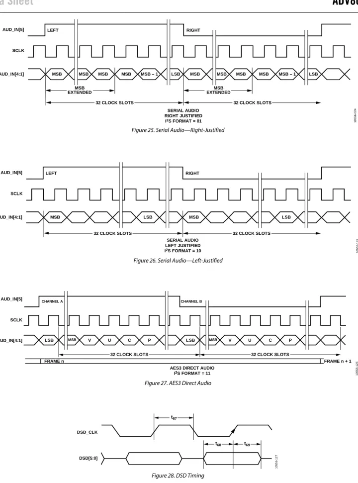
AUD_IN[5] SCLK AUD_IN[4:1] MSB MSB MSB MSB MSB – 1 LSB MSB MSB MSB MSB MSB – 1 LSB LEFT RIGHT SERIAL AUDIO RIGHT JUSTIFIED I2S FORMAT = 01 MSB EXTENDED MSB EXTENDED
32 CLOCK SLOTS 32 CLOCK SLOTS
10556-024
Figure 25. Serial Audio—Right-Justified
AUD_IN[5] SCLK AUD_IN[4:1] MSB LSB MSB LSB LEFT RIGHT SERIAL AUDIO LEFT JUSTIFIED I2S FORMAT = 10
32 CLOCK SLOTS 32 CLOCK SLOTS
10556-125
Figure 26. Serial Audio—Left-Justified
AUD_IN[5]
SCLK
AUD_IN[4:1]
CHANNEL A CHANNEL B
AES3 DIRECT AUDIO I2S FORMAT = 11
FRAME n + 1 FRAME n
32 CLOCK SLOTS 32 CLOCK SLOTS
P C U V P C U MSB V MSB LSB LSB 10556-126
Figure 27. AES3 Direct Audio
t67 t69 t68 DSD_CLK DSD[5:0] 10556-127 Figure 28. DSD Timing
ABSOLUTE MAXIMUM RATINGS
Table 5.
Parameter Rating
AVDD1, ADDD2, DVDD_IO to GND 3.9 V DVDD, PVDDx, CVDD1, AVDD3,
DVDD_DDR, PVDD_DDR to GND
2.2 V
DVDD to Other 1.8 V Power Supplies1 −0.3 V to +0.3 V
PVDD1 to Other 1.8 V Power Supplies1 −0.3 V to +0.3 V
PVDD2 to Other 1.8 V Power Supplies1 −0.3 V to +0.3 V
PVDD3 to Other 1.8 V Power Supplies1 −0.3 V to +0.3 V
PVDD5 to Other 1.8 V Power Supplies1 −0.3 V to +0.3 V
PVDD6 to Other 1.8 V Power Supplies1 −0.3 V to +0.3 V
CVDD1 to Other 1.8 V Power Supplies1 −0.3 V to +0.3 V
AVDD3 to Other 1.8 V Power Supplies1 −0.3 V to +0.3 V
DVDD_DDR to Other 1.8 V Power Supplies1 −0.3 V to +0.3 V PVDD_DDR to Other 1.8 V Power Supplies1 −0.3 V to +0.3 V
Digital Inputs to GND −0.3 V to DVDD_IO + 0.3 V Serial Video Inputs to GND −0.3 V to CVDD1 + 0.3 V DDR_IO and DDR_VREF to GND −0.3 V to DVDD_DDR + 0.3 V 5 V Tolerant Digital Inputs to GND2 −0.3 V to +5.5 V
1.8 V Analog Inputs to GND −0.3 V to AVDD3 + 0.3 V 3.3 V Analog Inputs to GND −0.3 V to AVDD2 + 0.3 V HDMI Digital Outputs to GND −0.3 V to AVDD3 + 0.3 V Digital Outputs Voltage to GND −0.3 V to DVDD_IO + 0.3 V Analog Outputs Voltage to GND3 −0.3 V to AVDD2 + 0.3 V
Maximum Junction Temperature (TJMAX) 125°C
Storage Temperature Range −65°C to+150°C Infrared Reflow Soldering (20 sec) 260°C
1 1.8 V power supplies include DVDD, PVDD1, PVDD2, PVDD3, PVDD5, PVDD6, CVDD1, AVDD3, DVDD_DDR, and PVDD_DR.
2 The following inputs are 5 V tolerant: CEC1, CEC2, DDC1_SCL, DDC2_SCL, DDC1_SDA, DDC2_SDA, HEAC_1−, HEAC_1+, HEAC_2−, HEAC_2+, RX_5V, and RX_HPD.
3 Except the ELPF1 and ELPF2 outputs, which are kept to −0.3 V to PVDD3 + 0.3 V; the RTERM output, which is kept to −0.3 V to CVDD1 + 0.3 V; and the R_TX1 and R_TX2 outputs, which are kept to −0.3 V to PVDD5 + 0.3 V.
Stresses above those listed under Absolute Maximum Ratings
may cause permanent damage to the device. This is a stress
rating only; functional operation of the device at these or any
other conditions above those indicated in the operational
section of this specification is not implied. Exposure to absolute
maximum rating conditions for extended periods may affect
device reliability.
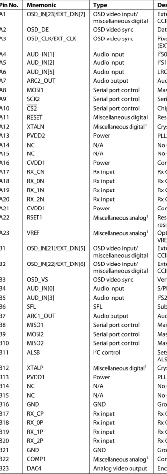
PIN CONFIGURATION AND FUNCTION DESCRIPTIONS
VREF RSET1 CVDD1 RX_2N RX_1N RX_0N RX_CN CVDD1 NC PVDD2 XTALN RESET CS2 SCK2 MOSI1 ARC2_ OUT AUD_ IN[5] AUD_ IN[2] AUD_ IN[1] DAC4 COMP1 GND RX_2P RX_1P RX_0P RX_CP GND NC PVDD1 XTALP ALSB MISO2 MOSI2 MISO1 ARC1_ OUT SFL NC NC AUD_ IN[3] AUD_ IN[0] DAC6 DAC5 AVDD1 AVDD1 GND GND AVDD1 RX_ HPD NC GND GND PDN INT0 GND SCK1 SCL SCLK DSD_ CLK AUD_ IN[4] GND DAC2 DAC1 AVDD2 AVDD2 RTERM NC NC RX_5V NC NC NC NC NC TEST1 DVDD_ IO INT2 INT1 GND CS1 SDA MCLK DVDD_ IO GND AVDD3 GND ELPF2 ELPF1 CEC1 GND PVDD3 RSET2 DAC3 COMP2 GND TEST2 GND GND GND GND DVDD GND GND DVDD GND GND GND OSD_ IN[8] OSD_ IN[7] OSD_ IN[6] OSD_ IN[5] TX1_2– TX1_2+ GND GND GND GND GND GND GND GND GND GND GND GND GND OSD_ IN[4] OSD_ IN[3] OSD_ IN[2] OSD_ IN[1] TX1_1– TX1_1+ GND DDC1_ SDA DVDD GND GND GND GND GND GND GND GND GND DVDD OSD_ IN[0] OSD_ HS HS DE TX1_0– TX1_0+ GND DDC1_ SCL GND GND GND GND GND GND GND GND GND GND GND DVDD_ IO DVDD_ IO PCLK VS TX1_C– TX1_C+ GND HPD_ TX1 GND GND GND GND GND GND GND GND GND GND DVDD P[35] P[34] P[33] P[32] HEAC_ 1– HEAC_ 1+ PVDD5 R_TX1 GND GND GND GND GND GND GND GND GND GND GND GND GND GND GND GND GND GND GND GND GND GND GND GND GND GND GND GND GND GND GND GND GND GND GND GND GND GND GND GND GND GND GND GND GND GND GND GND GND GND GND GND GND GND GND GND GND GND GND GND GND P[31] P[30] P[29] P[28] AVDD3 PVDD5 CEC2 P[27] P[26] P[25] P[24] TX2_2– TX2_2+ GND DDC2_ SCL DVDD DVDD P[23] P[22] P[21] P[20] TX2_1– TX2_1+ GND DDC2_ SDA P[19] P[18] P[17] P[16] TX2_0– TX2_0+ GND HPD_ TX2 GND GND P[15] P[14] TX2_C– TX2_C+ GND R_TX2 HEAC_ 2– HEAC_ 2+ PVDD6 GND AVDD3 PVDD6 TEST3 GND DDR_ DQ[6] GND DVDD DVDD DVDD DDR_ DQ[9] DDR_ DQ[14] GND GND DDR_ A[4] DDR_ A[11] GND DDR_ DQS[3] DDR_ DQ[23] PVDD_ DDR DVDD_ DDR DDR_ CK DVDD_ DDR DDR_ CAS DVDD_ DDR DVDD_ DDR P[13] P[12] P[11] P[10] P[9] P[8] P[7] P[6] P[5] P[4] P[3] P[2] GND DDR_ DQS[2] P[1] P[0] DDR_ DQ[3] GND GND DDR_ DM[0] DDR_ DQ[11] DDR_ DM[1] DVDD_ DDR GND DDR_ CK DVDD_ DDR DDR_ CS GND DDR_ A[2] DVDD_ DDR DDR_ A[8] NC/ GND DDR_ DQS[3] DDR_ DQ[26] DVDD_ DDR DDR_ DQS[2] GND GND DDR_ DQ[18] DDR_ DQ[4] DDR_ DQS[0] DDR_ DQ[5] DDR_ DQ[0] DDR_ DQS[1] DDR_ DQ[13] DDR_ DQ[8] DDR_ DQ[12] DDR_ CKE DDR_ RAS DDR_ BA[0] DDR_ A[0] DDR_ A[3] DDR_ A[6] DDR_ A[12] DDR_ DQ[29] DDR_ DQ[31] DDR_ DQ[30] DDR_ DM[3] DDR_ DM[2] DDR_ DQ[17] DDR_ DQ[19] DDR_ DQ[21] DDR_ DQ[1] DDR_ DQS[0] DDR_ DQ[2] DDR_ DQ[7] DDR_ DQ[10] DDR_ DQ[15] DDR_ DQS[1] DDR_ VREF DDR_ WE DDR_ BA[2] DDR_ BA[1] DDR_ A[10] DDR_ A[1] DDR_ A[7] DDR_ A[5] DDR_ A[9] DDR_ DQ[24] DDR_ DQ[28] DDR_ DQ[27] DDR_ DQ[25] DDR_ DQ[22] DDR_ DQ[20] DDR_ DQ[16] OSD_ IN[12] OSD_ IN[11] OSD_ IN[10] OSD_ IN[9] DVDD_ IO OSD_ VS OSD_ DE A B C D E F G H J K L M N P R T U V W Y AA AB AC A B C D E F G H J K L M N P R T U V W Y AA AB AC 1 2 3 4 5 6 7 8 9 10 11 12 13 14 15 16 17 18 19 20 21 22 23 1 2 3 4 5 6 7 8 9 10 11 12 13 14 15 16 17 18 19 20 21 22 23 OSD_ IN[23]/ EXT_ DIN[7] OSD_ CLK/ EXT_ CLK OSD_ IN[21]/ EXT_ DIN[5] OSD_ IN[22]/ EXT_ DIN[6] OSD_ IN[19]/ EXT_ DIN[3] OSD_ IN[20]/ EXT_ DIN[4] OSD_ IN[16]/ EXT_ DIN[0] OSD_ IN[17]/ EXT_ DIN[1] OSD_ IN[18]/ EXT_ DIN[2] OSD_ IN[13]/ VBI_SCK OSD_ IN[14]/ VBI_MOSI OSD_ IN[15]/ VBI_CS 10556-025Table 6. ADV8003KBCZ-8 and ADV8003KBCZ-7 Pin Function Descriptions
Pin No. Mnemonic Type Description
A1 OSD_IN[23]/EXT_DIN[7] OSD video input/ miscellaneous digital
External OSD Video Pixel Input Port (OSD_IN[23])/Additional TTL Input for External CCIR 656 Video Data (EXT_DIN[7]).
A2 OSD_DE OSD video sync Data Enable for the OSD Input Port.
A3 OSD_CLK/EXT_CLK OSD video sync Pixel Clock for the OSD Input Port (OSD_CLK)/Pixel Clock for External Video Data (EXT_CLK).
A4 AUD_IN[1] Audio input I2S0/DSD1 Audio Input.
A5 AUD_IN[2] Audio input I2S1/DSD2 Audio Input.
A6 AUD_IN[5] Audio input LRCLK/DSD5 Audio Input.
A7 ARC2_OUT Audio output Audio Return Channel for HDMI Tx2.
A8 MOSI1 Serial port control Master Out Slave In (Serial Port 1). Serial Port 1 is used for OSD control. A9 SCK2 Serial port control Serial Clock (Serial Port 2). Serial Port 2 is used for the external flash ROM. A10 CS2 Serial port control Chip Select (Serial Port 2). Serial Port 2 is used for the external flash ROM. A11 RESET Miscellaneous digital Reset Pin.
A12 XTALN Miscellaneous digital1 Crystal Input.
A13 PVDD2 Power PLL Digital Supply Voltage (1.8 V).
A14 NC N/A No Connect. Do not connect to this pin.
A15 NC N/A No Connect. Do not connect to this pin.
A16 CVDD1 Power Comparator Supply Voltage (1.8 V).
A17 RX_CN Rx input Rx Clock Complement Input.
A18 RX_0N Rx input Rx Channel 0 Complement Input.
A19 RX_1N Rx input Rx Channel 1 Complement Input.
A20 RX_2N Rx input Rx Channel 2 Complement Input.
A21 CVDD1 Power Comparator Supply Voltage (1.8 V).
A22 RSET1 Miscellaneous analog1 Resistor Current Setting for Encoder DACs: DAC1, DAC2, and DAC3. Place the RSET1
resistor as close as possible to the ADV8003.
A23 VREF Miscellaneous analog1 Optional External Voltage Reference Input for DACs or Voltage Reference Output. Place
VREF voltage components as close as possible to the ADV8003. B1 OSD_IN[21]/EXT_DIN[5] OSD video input/
miscellaneous digital External OSD Video Pixel Input Port (OSD_IN[21])/Additional TTL Input for External CCIR 656 Video Data (EXT_DIN[5]). B2 OSD_IN[22]/EXT_DIN[6] OSD video input/
miscellaneous digital External OSD Video Pixel Input Port (OSD_IN[22])/Additional TTL Input for External CCIR 656 Video Data (EXT_DIN[6]). B3 OSD_VS OSD video sync Vertical Sync for the OSD Input Port.
B4 AUD_IN[0] Audio input S/PDIF/DSD0 Audio Input.
B5 AUD_IN[3] Audio input I2S2/DSD3 Audio Input.
B6 SFL SFL Subcarrier Frequency Lock Signal (SFL).
B7 ARC1_OUT Audio output Audio Return Channel for HDMI Tx1.
B8 MISO1 Serial port control Master In Slave Out (Serial Port 1). Serial Port 1 is used for OSD control. B9 MOSI2 Serial port control Master Out Slave In (Serial Port 2). Serial Port 2 is used for the external flash ROM. B10 MISO2 Serial port control Master In Slave Out (Serial Port 2). Serial Port 2 is used for the external flash ROM.
B11 ALSB I2C control Sets LSB of I2C address. When the ALSB pin is set low, the I2C address is 0x18; when the
ALSB pin is set high, the I2C address is 0x1A.
B12 XTALP Miscellaneous digital1 Crystal Input.
B13 PVDD1 Power PLL Analog Supply Voltage (1.8 V).
B14 NC N/A No Connect. Do not connect to this pin.
B15 NC N/A No Connect. Do not connect to this pin.
B16 GND GND Ground.
B17 RX_CP Rx input Rx Clock True Input.
B18 RX_0P Rx input Rx Channel 0 True Input.
B19 RX_1P Rx input Rx Channel 1 True Input.
B20 RX_2P Rx input Rx Channel 2 True Input.
B21 GND GND Ground.
B22 COMP1 Miscellaneous analog1 Compensation Pin. Connect a 2.2 nF capacitor from COMP1 to AVDD2.
Pin No. Mnemonic Type Description C1 OSD_IN[19]/EXT_DIN[3] OSD video input/
miscellaneous digital
External OSD Video Pixel Input Port (OSD_IN[19])/Additional TTL Input for External CCIR 656 Video Data (EXT_DIN[3]).
C2 OSD_IN[20]/EXT_DIN[4] OSD video input/
miscellaneous digital External OSD Video Pixel Input Port (OSD_IN[20])/Additional TTL Input for External CCIR 656 Video Data (EXT_DIN[4]).
C3 GND GND Ground.
C4 AUD_IN[4] Audio input I2S3/DSD4 Audio Input.
C5 DSD_CLK Audio input DSD Audio Clock Input.
C6 SCLK Audio input I2S Bit Clock Input.
C7 SCL I2C control I2C Clock Input. SCL is open drain; use a 4.7 kΩ resistor to connect this pin to a 3.3 V supply.
C8 SCK1 Serial port control Serial Clock (Serial Port 1). Serial Port 1 is used for OSD control.
C9 GND GND Ground.
C10 INT0 Miscellaneous digital Interrupt Pin 0. When status bits change, this pin is triggered. C11 PDN Miscellaneous digital Power-Down. This pin controls the power state of the ADV8003.
C12 GND GND Ground.
C13 GND GND Ground.
C14 NC N/A No Connect. Do not connect to this pin.
C15 NC N/A No Connect. Do not connect to this pin.
C16 RX_HPD Rx input Hot Plug Assert Signal Output for the Rx Input.
C17 AVDD1 Power HDMI Rx Inputs Analog Supply (3.3 V).
C18 GND GND Ground.
C19 GND GND Ground.
C20 AVDD1 Power HDMI Rx Inputs Analog Supply (3.3 V).
C21 AVDD1 Power HDMI Rx Inputs Analog Supply (3.3 V).
C22 DAC5 Analog video output Encoder DAC5 Output. C23 DAC6 Analog video output Encoder DAC6 Output. D1 OSD_IN[16]/EXT_DIN[0] OSD video input/
miscellaneous digital
External OSD Video Pixel Input Port (OSD_IN[16])/Additional TTL Input for External CCIR 656 Video Data (EXT_DIN[0]).
D2 OSD_IN[17]/EXT_DIN[1] OSD video input/ miscellaneous digital
External OSD Video Pixel Input Port (OSD_IN[17])/Additional TTL Input for External CCIR 656 Video Data (EXT_DIN[1]).
D3 OSD_IN[18]/EXT_DIN[2] OSD video input/
miscellaneous digital External OSD Video Pixel Input Port (OSD_IN[18])/Additional TTL Input for External CCIR 656 Video Data (EXT_DIN[2]).
D4 GND GND Ground.
D5 DVDD_IO Power Digital Interface Supply (3.3 V).
D6 MCLK Audio input MCLK for S/PDIF Input Audio.
D7 SDA I2C control I2C Data Input. SDA is open drain; use a 4.7 kΩ resistor to connect this pin to a 3.3 V supply.
D8 CS1 Serial port control Chip Select (Serial Port 1). Serial Port 1 is used for OSD control.
D9 GND GND Ground.
D10 INT1 Miscellaneous digital Interrupt Pin for HDMI Transmitter Outputs. When status bits change, an interrupt is generated on this pin.
D11 INT2 Miscellaneous digital Interrupt Pin for HDMI Receiver Input Lines. When status bits change, an interrupt is generated on this pin.
D12 DVDD_IO Power Digital Interface Supply (3.3 V).
D13 TEST1 Miscellaneous digital Test Pin. Float this pin.
D14 NC N/A No Connect. Do not connect to this pin.
D15 NC N/A No Connect. Do not connect to this pin.
D16 RX_5V Rx input 5 V Detect Pin for the Rx Input.
D17 NC N/A No Connect. Do not connect to this pin.
D18 NC N/A No Connect. Do not connect to this pin.
D19 RTERM HDMI Rx input This pin sets internal termination resistance. Use a 500 Ω resistor between this pin and GND. Place the RTERM resistor as close as possible to the ADV8003.
D20 AVDD2 Power Analog Power Supply (3.3 V).
D21 AVDD2 Power Analog Power Supply (3.3 V).
Pin No. Mnemonic Type Description E1 OSD_IN[13]/VBI_SCK OSD video input/
miscellaneous digital
External OSD Video Pixel Input Port (OSD_IN[13])/Serial Clock for VBI Data Serial Port (VBI_SCK).
E2 OSD_IN[14]/VBI_MOSI OSD video input/
miscellaneous digital External OSD Video Pixel Input Port (OSD_IN[14])/Master Out Slave In for VBI Data Serial Port (VBI_MOSI). E3 OSD_IN[15]/VBI_CS OSD video input/
miscellaneous digital External OSD Video Pixel Input Port (OSD_IN[15])/Chip Select for VBI Data Serial Port (VBI_CS).
E4 DVDD_IO Power Digital Interface Supply (3.3 V).
E20 TEST2 Miscellaneous analog Test Pin. Float this pin.
E21 GND GND Ground.
E22 COMP2 Miscellaneous analog1 Compensation Pin. Connect a 2.2 nF capacitor to AVDD2.
E23 DAC3 Analog video output Encoder DAC3 Output.
F1 OSD_IN[9] OSD video input External OSD Video Pixel Input Port (OSD_IN[9]). F2 OSD_IN[10] OSD video input External OSD Video Pixel Input Port (OSD_IN[10]). F3 OSD_IN[11] OSD video input External OSD Video Pixel Input Port (OSD_IN[11]).
F4 OSD_IN[12] OSD video input/
miscellaneous digital
External OSD Video Pixel Input Port (OSD_IN[12]).
F20 RSET2 Miscellaneous analog1 Resistor Current Setting for Encoder DACs: DAC4, DAC5, and DAC6. Place the RSET2
resistor as close as possible to the ADV8003.
F21 PVDD3 Power PLL Supply (1.8 V).
F22 GND GND Ground.
F23 CEC1 HDMI Tx1 HDMI Tx1 Consumer Electronics Control (CEC).
G1 OSD_IN[5] OSD video input External OSD Video Pixel Input Port (OSD_IN[5]). G2 OSD_IN[6] OSD video input External OSD Video Pixel Input Port (OSD_IN[6]). G3 OSD_IN[7] OSD video input External OSD Video Pixel Input Port (OSD_IN[7]). G4 OSD_IN[8] OSD video input External OSD Video Pixel Input Port (OSD_IN[8]).
G7 GND GND Ground.
G8 GND GND Ground.
G9 GND GND Ground.
G10 DVDD Power Digital Power Supply (1.8 V).
G11 GND GND Ground.
G12 GND GND Ground.
G13 DVDD Power Digital Power Supply (1.8 V).
G14 GND GND Ground.
G15 GND GND Ground.
G16 GND GND Ground.
G17 GND GND Ground.
G20 ELPF1 Miscellaneous analog1 External Loop Filter for PLL 1. Connect to PVDD3.
G21 ELPF2 Miscellaneous analog1 External Loop Filter for PLL 2. Connect to PVDD3.
G22 GND GND Ground.
G23 AVDD3 Power HDMI Analog Power Supply (1.8 V).
H1 OSD_IN[1] OSD video input External OSD Video Pixel Input Port (OSD_IN[1]). H2 OSD_IN[2] OSD video input External OSD Video Pixel Input Port (OSD_IN[2]). H3 OSD_IN[3] OSD video input External OSD Video Pixel Input Port (OSD_IN[3]). H4 OSD_IN[4] OSD video input External OSD Video Pixel Input Port (OSD_IN[4]).
H7 GND GND Ground. H8 GND GND Ground. H9 GND GND Ground. H10 GND GND Ground. H11 GND GND Ground. H12 GND GND Ground. H13 GND GND Ground. H14 GND GND Ground. H15 GND GND Ground. H16 GND GND Ground. H17 GND GND Ground. H20 GND GND Ground.
Pin No. Mnemonic Type Description
H21 GND GND Ground.
H22 TX1_2+ HDMI Tx1 HDMI1 Channel 2 True Output.
H23 TX1_2− HDMI Tx1 HDMI1 Channel 2 Complementary Output.
J1 DE Digital video sync Data Enable for Digital Input Video. J2 HS Digital video sync Horizontal Sync for Digital Input Video.
J3 OSD_HS Digital video sync Horizontal Sync for the OSD Input Port (OSD_HS). J4 OSD_IN[0] OSD video input External OSD Video Pixel Input Port (OSD_IN[0]).
J7 DVDD Power Digital Power Supply (1.8 V).
J8 GND GND Ground. J9 GND GND Ground. J10 GND GND Ground. J11 GND GND Ground. J12 GND GND Ground. J13 GND GND Ground. J14 GND GND Ground. J15 GND GND Ground. J16 GND GND Ground.
J17 DVDD Power Digital Power Supply (1.8 V).
J20 DDC1_SDA HDMI Tx1 HDCP Slave Serial Data for HDMI Tx1. This pin is open drain; use a 2 kΩ resistor to connect this pin to the HDMI Tx 5 V supply.
J21 GND GND Ground.
J22 TX1_1+ HDMI Tx1 HDMI1 Channel 1 True Output.
J23 TX1_1− HDMI Tx1 HDMI1 Channel 1 Complementary Output.
K1 VS Digital video sync Vertical Sync for Digital Input Video. K2 PCLK Digital video sync Pixel Clock for Digital Input Video.
K3 DVDD_IO Power Digital Interface Supply (3.3 V).
K4 DVDD_IO Power Digital Interface Supply (3.3 V).
K7 GND GND Ground. K8 GND GND Ground. K9 GND GND Ground. K10 GND GND Ground. K11 GND GND Ground. K12 GND GND Ground. K13 GND GND Ground. K14 GND GND Ground. K15 GND GND Ground. K16 GND GND Ground. K17 GND GND Ground.
K20 DDC1_SCL HDMI Tx1 HDCP Slave Serial Clock for HDMI Tx1. This pin is open drain; use a 2 kΩ resistor to connect this pin to the HDMI Tx 5 V supply.
K21 GND GND Ground.
K22 TX1_0+ HDMI Tx1 HDMI1 Channel 0 True Output.
K23 TX1_0− HDMI Tx1 HDMI1 Channel 0 Complementary Output.
L1 P[32] Digital video input Digital Video Input Bus[35:0]. L2 P[33] Digital video input Digital Video Input Bus[35:0]. L3 P[34] Digital video input Digital Video Input Bus[35:0]. L4 P[35] Digital video input Digital Video Input Bus[35:0].
L7 DVDD Power Digital Power Supply (1.8 V).
L8 GND GND Ground. L9 GND GND Ground. L10 GND GND Ground. L11 GND GND Ground. L12 GND GND Ground. L13 GND GND Ground. L14 GND GND Ground.
Pin No. Mnemonic Type Description
L16 GND GND Ground.
L17 GND GND Ground.
L20 HPD_TX1 HDMI Tx1 Hot Plug Assert Signal Input for HDMI Tx1.
L21 GND GND Ground.
L22 TX1_C+ HDMI Tx1 HDMI1 Clock True Output.
L23 TX1_C− HDMI Tx1 HDMI1 Clock Complementary Output.
M1 P[28] Digital video input Digital Video Input Bus[35:0]. M2 P[29] Digital video input Digital Video Input Bus[35:0]. M3 P[30] Digital video input Digital Video Input Bus[35:0]. M4 P[31] Digital video input Digital Video Input Bus[35:0].
M7 GND GND Ground. M8 GND GND Ground. M9 GND GND Ground. M10 GND GND Ground. M11 GND GND Ground. M12 GND GND Ground. M13 GND GND Ground. M14 GND GND Ground. M15 GND GND Ground. M16 GND GND Ground. M17 GND GND Ground.
M20 R_TX1 HDMI Tx11 Sets Internal Reference Currents. Place a 470 Ω resistor (1% tolerance) between this pin and
ground, as close as possible to the ADV8003.
M21 PVDD5 Power1 HDMI Tx PLL Power Supply (1.8 V).
M22 HEAC_1+ HDMI Tx1 HDMI Tx1 HEAC+ from the HDMI Connector.
M23 HEAC_1− HDMI Tx1 HDMI Tx1 HEAC− from the HDMI Connector.
N1 P[24] Digital video input Digital Video Input Bus[35:0]. N2 P[25] Digital video input Digital Video Input Bus[35:0]. N3 P[26] Digital video input Digital Video Input Bus[35:0]. N4 P[27] Digital video input Digital Video Input Bus[35:0].
N7 GND GND Ground. N8 GND GND Ground. N9 GND GND Ground. N10 GND GND Ground. N11 GND GND Ground. N12 GND GND Ground. N13 GND GND Ground. N14 GND GND Ground. N15 GND GND Ground. N16 GND GND Ground. N17 GND GND Ground.
N20 CEC2 HDMI Tx2 HDMI Tx2 Consumer Electronics Control (CEC).
N21 PVDD5 Power1 HDMI Tx PLL Power Supply (1.8 V).
N22 AVDD3 Power HDMI Analog Power Supply (1.8 V).
N23 NC N/A No Connect. Do not connect to this pin.
P1 P[20] Digital video input Digital Video Input Bus[35:0]. P2 P[21] Digital video input Digital Video Input Bus[35:0]. P3 P[22] Digital video input Digital Video Input Bus[35:0]. P4 P[23] Digital video input Digital Video Input Bus[35:0].
P7 DVDD Power Digital Power Supply (1.8 V).
P8 GND GND Ground. P9 GND GND Ground. P10 GND GND Ground. P11 GND GND Ground. P12 GND GND Ground. P13 GND GND Ground.
Pin No. Mnemonic Type Description
P14 GND GND Ground.
P15 GND GND Ground.
P16 GND GND Ground.
P17 DVDD Power Digital Power Supply (1.8 V).
P20 DDC2_SCL HDMI Tx2 HDCP Slave Serial Clock for HDMI Tx2. This pin is open drain; use a 2 kΩ resistor to connect this pin to the HDMI Tx 5 V supply.
P21 GND GND Ground.
P22 TX2_2+ HDMI Tx2 HDMI2 Channel 2 True Output.
P23 TX2_2− HDMI Tx2 HDMI2 Channel 2 Complementary Output.
R1 P[16] Digital video input Digital Video Input Bus[35:0]. R2 P[17] Digital video input Digital Video Input Bus[35:0]. R3 P[18] Digital video input Digital Video Input Bus[35:0]. R4 P[19] Digital video input Digital Video Input Bus[35:0].
R7 GND GND Ground. R8 GND GND Ground. R9 GND GND Ground. R10 GND GND Ground. R11 GND GND Ground. R12 GND GND Ground. R13 GND GND Ground. R14 GND GND Ground. R15 GND GND Ground. R16 GND GND Ground. R17 GND GND Ground.
R20 DDC2_SDA HDMI Tx2 HDCP Slave Serial Data for HDMI Tx2. This pin is open drain; use a 2 kΩ resistor to connect this pin to the HDMI Tx 5 V supply.
R21 GND GND Ground.
R22 TX2_1+ HDMI Tx2 HDMI2 Channel 1 True Output.
R23 TX2_1− HDMI Tx2 HDMI2 Channel 1 Complementary Output.
T1 P[14] Digital video input Digital Video Input Bus[35:0]. T2 P[15] Digital video input Digital Video Input Bus[35:0].
T3 GND GND Ground. T4 GND GND Ground. T7 GND GND Ground. T8 GND GND Ground. T9 GND GND Ground. T10 GND GND Ground. T11 GND GND Ground. T12 GND GND Ground. T13 GND GND Ground. T14 GND GND Ground. T15 GND GND Ground. T16 GND GND Ground. T17 GND GND Ground.
T20 HPD_TX2 HDMI Tx2 Hot Plug Assert Signal Input for HDMI Tx2.
T21 GND GND Ground.
T22 TX2_0+ HDMI Tx2 HDMI2 Channel 0 True Output.
T23 TX2_0− HDMI Tx2 HDMI2 Channel 0 Complementary Output.
U1 P[10] Digital video input Digital Video Input Bus[35:0]. U2 P[11] Digital video input Digital Video Input Bus[35:0]. U3 P[12] Digital video input Digital Video Input Bus[35:0]. U4 P[13] Digital video input Digital Video Input Bus[35:0].
U7 GND GND Ground.
U8 GND GND Ground.
Pin No. Mnemonic Type Description
U11 GND GND Ground.
U12 DVDD Power Digital Power Supply (1.8 V).
U13 GND GND Ground.
U14 GND GND Ground.
U15 DVDD Power Digital Power Supply (1.8 V).
U16 GND GND Ground.
U17 GND GND Ground.
U20 R_TX2 HDMI Tx21 Sets internal reference currents. Place a 470 Ω resistor (1% tolerance) between this pin
and ground, as close as possible to the ADV8003.
U21 GND GND Ground.
U22 TX2_C+ HDMI Tx21 HDMI2 Clock True Output.
U23 TX2_C− HDMI Tx21 HDMI2 Clock Complementary Output.
V1 P[6] Digital video input Digital Video Input Bus[35:0]. V2 P[7] Digital video input Digital Video Input Bus[35:0]. V3 P[8] Digital video input Digital Video Input Bus[35:0]. V4 P[9] Digital video input Digital Video Input Bus[35:0].
V20 GND GND Ground.
V21 PVDD6 Power1 HDMI Tx PLL Power Supply (1.8 V).
V22 HEAC_2+ HDMI Tx2 HDMI Tx2 HEC+ from HDMI Connector.
V23 HEAC_2− HDMI Tx2 HDMI Tx2 HEC− from HDMI Connector.
W1 P[2] Digital video input Digital Video Input Bus[35:0]. W2 P[3] Digital video input Digital Video Input Bus[35:0]. W3 P[4] Digital video input Digital Video Input Bus[35:0]. W4 P[5] Digital video input Digital Video Input Bus[35:0].
W20 TEST3 Miscellaneous digital Test Pin. Connect this pin to ground through a 0.1 µF capacitor.
W21 PVDD6 Power1 HDMI Tx PLL Power Supply (1.8 V).
W22 AVDD3 Power HDMI Analog Power Supply (1.8 V).
W23 NC N/A No Connect. Do not connect to this pin.
Y1 P[0] Digital video input Digital Video Input Bus[35:0]. Y2 P[1] Digital video input Digital Video Input Bus[35:0].
Y3 DDR_DQS[2] DDR interface Data Strobe for DDR Data Bytes[23:16].
Y4 GND GND Ground.
Y5 DDR_DQ[23] DDR interface Data Line. Interface to external RAM data lines.
Y6 DVDD_DDR Power DDR Interface Supply (1.8 V).
Y7 DDR_DQS[3] DDR interface Data Strobe for DDR Data Bytes[31:24].
Y8 GND GND Ground.