Gas Sensing Using One-Dimensional Photonic Crystal
Nanoresonators
Oumayma Habli1, Yassine Bouazzi1, 2, *, and Mounir Kanzari1, 3
Abstract—In recent years, there has been more research on the use of photonic crystals PCs in the field of detection. The application of these materials as gas sensors seems very promising, because of their miniaturization and high spectral sensitivities. The aim of this work is to contribute to the design and study of a resonant microsystem based on one-dimensional photonic crystals for applications such as optical devices with high quality factor for detecting and measuring the concentration of gas in the air. Indeed, we have proposed a gas monitoring structure. This nanosystem is formed by an alternating stack of silicon Si layers and air with a resonant nanocavity in the middle. The numerical results show that the resonance peak that appears on the Photonic Band Gap (PBG) is caused by the creation of the nanocavity within the periodic 1D structure. This resonance peak can be used as a reference for real-time detection and environmental monitoring. In addition, we theoretically studied the relevance of these photonic systems and analyzed the effect of the intrinsic and extrinsic parameters of this device on the detection performance. We have also tried to improve the performance of such a device for the effect study of the inclination variation of the radiation incidence source on the selectivity of the detector.
1. INTRODUCTION
Photonic crystals (PCs) are artificial materials made from periodic arrays of dielectric or metallic building blocks. The existence of photonic band gaps (PBGs) has brought about an unprecedented power to control and manipulate the propagation of electromagnetic (EM) waves [1–3]. The simplest form of a photonic crystal is a one-dimensional periodic structure. It is known as the Bragg mirror. It consists of a stack of alternating layers having a low and a high refractive indices whose thicknesses satisfy the Bragg condition: nH·dH =nL·dL= λ4, whereλis the reference wavelength [4]. In contrast
to the two- and three-dimensional cases, the one-dimensional photonic crystal is attractive since its production is more feasible at any wavelength scale. The first function of a PBG is to be an excellent reflective mirror (more than 99(%)). Therefore, one option for providing a more flexible design of band gap structures could be to increase the width of the PBGs. In recent years, there have been several research works on the use of photonic crystals on the topic of sensor [5–7]. The application of photonic crystals as gas sensors in the area of research seems very promising due to their miniaturization and high spectral sensitivity. In this work we will show that one-dimensional (1D) photonic crystal formed by alternating layers of Silicon (Si) and Air with an empty “defect” layer in the middle can be used as an optical sensor for measuring the concentration of gases in air when it is illuminated by light in normal incidence.
Received 11 January 2019, Accepted 7 March 2019, Scheduled 27 May 2019
* Corresponding author: Yassine Bouazzi (yassine.bouazzi@enit.utm.tn).
1 Laboratory of Photovoltaic and Semi-conductor Materials, National Engineering School of Tunis, EL Manar University,
2. FORMULATION METHOD
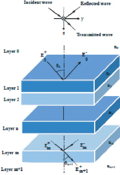
The Transfer Matrix Method (TMM) approach is a matrix method particularly well suitable for the study of PBG materials, which can solve the standard problem of the photonic band gap structures and the scattering (transmission, reflection, and absorption) spectrum [8]. It is based on the Abeles approach in terms of forward and backward propagating electric fields,E0+andE0−, which are introduced
to calculate the reflection and transmission. The optical configuration used for incident and reflected fields is described in Fig. 1.
Figure 1. Incident and reflected fields for a 1D multilayer structure.
Abeles showed that the relation between the amplitudes [8] of the electric fields of the incident wave Em++1 is expressed as the following matrix for stratified films withinm layers:
E0+
E0−
=
T11 T12
T21 T22
Em++1
Em−+1
(1)
Equation (1) holds whatever the boundary conditions. The reflection and transmission coefficients in complex amplitude are, from the left to the right (By setting, because there is no reflection from the final phase) [9].
r= E
−
0
E0+
E− m+1=0
= T21
T11, t
= E
+
m+1
E0+
Em−+1=0
= 1
T11
(2)
and from the right to the left (E0+ = 0):
r = E
+
m+1
Em−+1
E+ 0=0
= −T12
T11 , t
= E0−
Em++1
E+ 0=0
= det[T]
T11
Unless specified otherwise, we limit ourselves to the case where the two semi-infinite media surrounding the structure are identical (n0 =nm+ 1), in which case, det[T] = 1. From a physical point of view, this
restriction does not change anything but presents the advantage of keeping formal expressions simpler to handle [9]. In intensity, the transmittance and reflectance are accordingly:
T = T =|t|2 = 1
T11
2 (4)
R = |r|2 =T21
T11
2 (5)
R = |r|2=T12
T11
2 (6)
3. RESULTS AND DISCUSSIONS
3.1. Effects of the Number of Layers
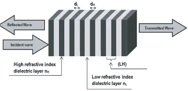
In this part, using a simulation script based on the TMM method we study the effects of the variation of the repetition numberJ of the pattern (LH) on the spectral behavior of a periodic multilayer system of the form H(LH)J (Fig. 2), where H denotes the layer of Titanium Dioxide (TiO2) with refractive
index nH = 2.3 and thickness dH = 4λnH0 , and L is the Silicon Dioxide (SiO2) layer with nL = 1.45
and thickness dL= 4λnL0 . This structure is illuminated in normal incidence with a NIR laser diode with central wavelength λ= 1.573µm [10] which sweeps between 6349 and 6365 cm−1.
Figure 2. Bragg mirror constructed with two types of layers, with indices of refraction respectively
nL(L) andnH(H) according to the distributionH(LH)J whereJ presents the number of period of the pattern (LH).
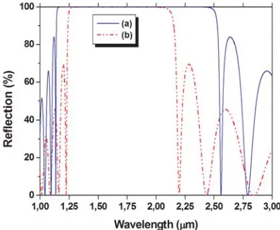
Fig. 3 shows the spectra of optical reflections, in the spectral domain [1µm, 3µm] with normal incidence and for variables repetitions numbersJ.
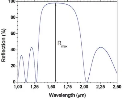
The spectra presented in Fig. 4 show the system performance to know; a total reflection of 100% in the vicinity of the reference wavelengthλ0= 1.573µm with an increase in the widths of these PBGs,
as a function of the repetition numberJ of the elementary patterns (LH) of the photonic structure. In fact, from the 7th iteration, we observe a remarkable increase in the maximum reflectionRmax(%)
R over the entire spectral domain (Fig. 5), consequently the appearance of a perfect PBG covering the neighborhood of the reference wavelength λ0 = 1.573µm.
Moreover, it can be seen that the PBG is centered aroundλ0 = 1.573µm, and its width expands
J=3 J=4 J=5
J=6 J=7 J=8
Figure 3. Reflection spectra for periodic systems for different repetitions numbersJ.
Figure 4. Presentation of the maximum
reflection Rmax(%) on an optical spectrum.
Figure 5. Variation of the maximum reflection
Rmax(%) according to the number of repetitions
J.
Hence, in the rest of this work, we consider J = 7, and our study structure becomes H(LH)7, which has a minimum number of layers and a maximum reflection.
3.2. Effect of Index Contrast
The index contrast or optical contrast is defined as the ratio between the high and low refractive indices constituting the network. For a one-dimensional structure, the index contrast is given by [11]δ = nHnL.
Figure 6. Variation of the PBG width as a function of the number of repetitionsJ.
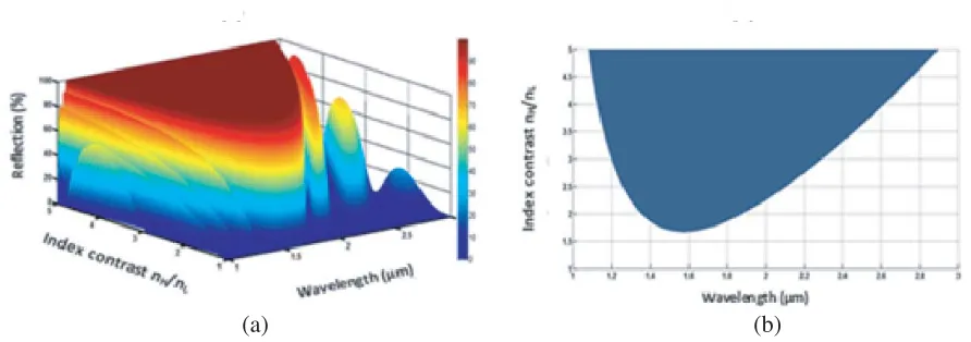
the high refractive index nH varied from 1 to 5. Then, we represented the optical reflections of the photonic structure. Also, we project the optical spectra obtained on the plane (OXY) to obtain the PBG mapping of the PBGs as a function of the index contrast δ.
Fig. 7 illustrates the optical reflections as a function of index contrast and wavelength as well as the maps of the corresponding bands, where the blue zone has the band gaps and the white zone the permitted bands.
(a) (b)
Figure 7. Spectral appearance as a function of the index contrast variation for a periodic multilayer structureH(LH)J: (a) Variation of reflection spectra as a function of index contrast, (b) Maps of PBGs as a function of the index contrast.
On the one hand, we note more particularly that the first PBG appears aroundλ0 = 1.573µm with
index contrastδ≈1.602. On the other hand, we find that the widths of the PBGs increase considerably with the index contrast. Also, a distance (divergence) of the backgrounds of the PBGs (λm) of the reference wavelength λ0 = 1.573µm as a function of the index contrast is observed. Table 1 gives the
variation of the width and position of the PBG in the vicinity of λ0 = 1.573µm, with λmin presenting
the lower limit of the band and λmax being the upper limit.
3.3. The Choice of the Initial Multilayer Structure
Table 1. Variation of the widths of the PBGs as well as their positions according to the index contrast.
δ= nHnL 2 2.5 3 3.5 4 4.5 5
λmax (µm) 1.875 2.105 2.293 2.460 2.617 2.763 2.898
λmin (µm) 1.355 1.258 1.195 1.155 1.125 1.097 1.063
λm (µm) 1.615 1.681 1.744 1.8075 1.871 1.93 1.980
ΔλP BG (µm) 0.520 0.847 1.098 1.305 1.492 1.666 1.835
In the previous parts we have shown that the number of optimal bilayers of the structure is equal to 7. Moreover, we have found that the width of the PBG increases according to the index contrast, so we can select the refractive index so that they provide a high contrast taking into account the availability of materials and their dielectric natures. So we chose the Silicon Si and the Air with refractive indexes respectivelynH = 3.4 andnL= 1.000256 (Fig. 8).
Figure 8. The chosen multilayer structure of type H(LH)7 with the elementary layers, respectively, Si (nH = 3.4) and air (nL= 1.000256).
Fig. 9 shows the reflection spectrum of the structure H(LH)7 with nH = 3.4 and nL= 1.000256 where we note that the PBG is wider than that for the multilayer with the same number of layers
H(LH)7 but with the refractive indices nH = 2.3 and nL= 1.000256.
3.4. Effect of Creating a Defect in 1D Periodic Multilayer Structure
3.4.1. Influence of the Presence of a Resonant Cavity on the Optical Properties in a Periodic 1D Multilayer Structure
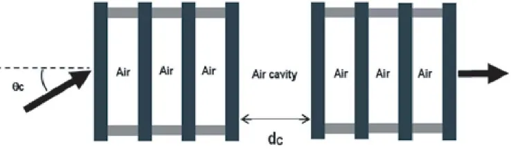
We consider a one-dimensional periodic photonic system of typeH(LH)J, with J keeping the optimal value J = 7. This structure is composed of a stack of silicon Si and Air layers which respectively correspond to the high and low index layers. In what follows, we introduce a defect, in the middle of the structure in the form of a thickness defect of the cavity (Fig. 9). In particular, we study the photometric properties of such type of hybrid system: H(LH)kC H(LH)kwithk= 3, whereCdenotes an air cavity of thicknessdC. In another way, as shown in Fig. 10, this system can be considered as two parallel Bragg mirrors arranged and spaced apart from each other by a distance dC.
Figure 10. One-dimensional photonic structure with the presence of a defect in the form of an air cavity.
To analyze this new hybrid nanosystem, we used the transfer matrix method (TMM), where we chose: The thickness of the high index layer (Si) and the low index layer (air), respectively:
dH = 4λ0
nH = 1.573
4×3.4 = 114.31 nm
dL = λ0 4nL =
1.573
4×1.000265 = 393.14 nm
In order to see the influence of the thickness on the spectral behavior of such a nanosystem, we have varied the cavity width from 600 nm to 800 nm. The transmission of the structure in question is shown in Fig. 11, for different widths of the cavity.
We can notice that the insertion of a cavity between two Bragg mirrors, the present case, results in the appearance of a resonance peak, characterizing a defect mode, which is positioned in the photonic band gap with a maximum intensity of 100%. It is also clear that as the width of the cavity dC increases, the position of the peak moves towards the high wavelengths (Table 2).
Table 2. Position of the resonance peak according to the width of the cavity.
Width of cavity dC (nm) 600 650 700 750 800
Position of the resonance peak (µm) 1.3157 1.382 1.4511 1.5215 1.5924
3.4.2. Choice of Parameters of the Detection Nanostructure
Figure 11. Transmission spectra of a 1D structure with air cavity, for dH = 114.31 nm and
dL = 393.14 nm with different width of the cavity: dC = 600 nm, dC = 650 nm, dC = 700 nm,
dC = 750 nm anddC = 800 nm.
resonant cavity dC. In addition, we proceeded to solve the problem from a point of view “purpose of use” of this optical device, that is to say, it is necessary to find a width dC to ensure a good detection quality. Indeed, like any resonant structure, our nanosystem will be characterized by a quality factor, generally denoted asQ. This quantity is defined as the ratio of the resonant wavelength peakλpeak by the Full Width at Half Maximum FWHM of the resonance peak peak Δλpeak
Q= λpeak
Δλpeak (7)
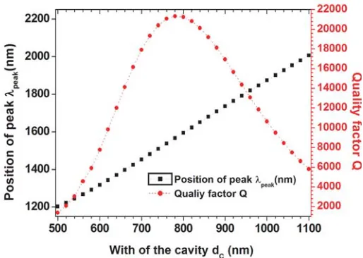
For this purpose, we measured the values of the peak position and the FWHM of the resonance peak, for each dC value which varies between 500 nm and 1100 nm. Similarly, we have calculated the quality factor Qon a step of 20 nm (Fig. 12).
From Fig. 12 we note that a slight variation in the width of the cavity dC causes a shift in the position of the resonance peakλpeak with an increase of the quality factorQ, until reaching a significant
value: Qmax = 21343 for a critical value dC = 780 nm which corresponds to resonance wavelength
λ=λ0 = 1.573µm. In addition, the quality factorQdecreases when the width of the cavitydC exceeds
the critical value. In sum, the position of the defect mode moves linearly towards the high wavelengths as a function of the width of cavity dC. Also, the quality factor decreases as the wavelength moves towards edges of the PBG.
These characteristics and this choice of geometrical parameters make the system a good candidate for the design of a high quality optical sensor with high sensitivity. So given all the above we can define the optimal geometrical parameters of our nanoresonator as:
- The thickness of the high index layer (Si): dH = 114.31 nm. - The thickness of the low index layer (air): dL= 393.14 nm. - The width of the nanocavity: dC = 780 nm.
3.5. Application of the Nanostructure for Gas Detection
After having shown that the photonic nanosystem in the previous part which presents a default mode is a monochromatic interference filter of “good quality”, we tried to apply this structure for the detection of gases. Indeed, we studied by simulating the effect of evacuation of a gas in the nanostructure cavity on the spectral behavior of the nanosystem. In other words, we analyzed the consequences of the change of air in the cavity by another polluting gas, i.e., the variation of the refractive index of the medium.
3.5.1. Result of the Detection Analysis
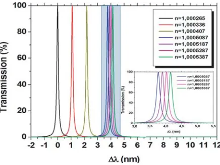
To study the mode of detection of the resonant cavity, we consider the most dominant pollutant gases in the nature of different refractive indices such as carbon monoxide CO (nCO = 1.0003360), carbon
dioxide CO2 (nCO2 = 1.000407), and nitrogen NO2 (nNO2 = 1.0005087). As a result, we illustrate
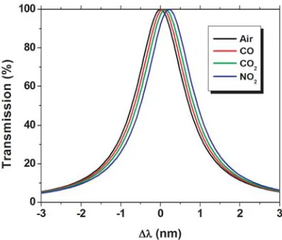
in Fig. 13, with a normal incidence, the transmission of the cavity mode for each type of gas as a function of displacement Δλrelative to the resonance wavelength of air that corresponds to the reference wavelength: Δλ=λ−λ0.
Figure 13. Transmission of the cavity mode for different gases where the air is a reference medium as a function of displacement Δλ=λ−λ0.
The transmission spectra denote, respectively, in black the resonance peak or the cavity mode for the reference medium (Air), in red the carbon oxide (CO), in green the carbon dioxide (CO2), and in
blue the nitrogen dioxide (NO2). Thus we observe a very small shift of the resonant peaks from the
Table 3. The displacement of the cavity mode Δλaccording to the nature of the polluting gas.
Gas Air CO CO2 NO2
Displacement Δλ(nm) 0 0.0634 0.1255 0.2156
3.5.2. Improvement of the Selectivity
In order to improve the spectral selectivity of the nanostructure, we note that any modification of the incident angle of the incoming beam causes a decrease in the full width at half maximum (FWHM) and a displacement of the resonance peaks in the band gap. Based on this effect we calculated the FWHM of the reference peak (Air) as a function of the incident angle with a step of 40π (Fig. 14).
Figure 14. Full width at half maximum of the defect mode (resonance peak) as a function of the incident angle varied from 0 rad to 1440πrad.
We notice that the FWHM decreases as the angle of incidenceθincreases, and the resonance peaks become narrower. Thus, the optical device becomes more selective than the use of the laser source in normal incidence. In addition, the FWHM of the resonance peak reaches a minimum of 0.08 nm for any angle of incidence greater than a critical angle θc = 1140π. In the rest of this part we considerθc as the angle of incidence of the laser source beam (Fig. 15).
Figure 15. The nanosystem of detection with oblique incidence of dC.
Table 4. The displacement of the cavity mode Δλaccording to the nature of the polluting gas.
Gas Air (reference) CO CO2 NO2
Displacement Δλ(nm) 0 1.0971 2.1939 3.7642
FWHM (pm) 174 160 170 184
Figure 16. Transmission and displacement of the cavity mode for different gases with air as the reference medium.
The FWHM of the cavity mode for the gases used has low values and varies as the nature of the gas: 174 pm for air, 160 pm for CO, 170 pm for CO2, and 184 pm for CO2. Therefore, by using a small
number of periodic layers in the proposed structure, it is possible to obtain a very narrow resonance peaks, i.e., the detection device has a good theoretical selectivity.
3.5.3. The Detection Efficiency
In what follows, we give an estimate of the efficiency of the sensor, by fixing the length of the resonant nanocavity dC at 780 nm, which offers the greatest sensitivity of the mode to the variation of the refractive index. We report the evolution of the transmission curves for a variation of the refractive index of the air polluted by nitrogen dioxide NO2 (nNO2 = 1.0005087) with a step of 10−5 (np = 1.0005087 to
np= 1.0005387) (Fig. 17).
Figure 17. The transmission spectra of the sensor with four different refractive indices varying from
We show that a variation of 10−5of the refractive index results in a shift of the cavity mode position equal to 132 pm. Thus we observe a good accuracy for cavity mode shift detection. In other words, a high accuracy of detection of change in the index of the cavity, i.e., the nature of the pollutant gas, is achieved.
3.5.4. Concentration and Sensitivity of Detection
In what follows and referring to the studies of Bouzidi et al. [12], we applied the previous analysis to a practical situation, by fixing the parameters of the resonant structure: dH = 114.31 nm,dL= 393.14 nm,
dC = 780 nm, and θc = 1140π. With these parameters, the operating wavelength of the sensor will be set to the reference wavelength λ0 = 1.573µm. The most common way to estimate the efficiency of a
sensor is to calculate its sensitivity given by the following expression:
S= Δλpeak
Δn (nm/RIU) (8)
In the following, we calculate the response of the sensor for the detection of the polluted air composed of different concentrations of Methane CH4 and Ethane C2H6. The refractive indices of different
concentrations are shown in Tables 5 and 6 of [13].
Fig. 18 represents the dependence of the resonance wavelengthλpeak with respect to the refractive index of the air polluted with methane (Fig. 18(a)) and ethane (Fig. 18(b)) for different concentrations.
Table 5. Refractive index of Methane nmix in air for different concentrations of Methane gaz CH4.
Methane CCH4 Cair nmix
5% 0.05 0.95 1.0000222 15% 0.15 0.85 1.0000666
Table 6. Refractive index of Ethane nmix in air for different concentrations of Ethane gaz C2H6.
Methane CC2H6 Cair nmix
3% 0.03 0.97 1.0000228 12.5% 0.125 0.875 1.000095
(a) (b)
Note that the resonance wavelength varies linearly with the refractive index where the slope represents the sensitivity with a value of 21688 nm/RIU. Indeed, a slight variation in the concentration of a polluting gas in the air can be detectable. So this type of sensor can be used to monitor the level of gas concentration in the ambient air.
4. CONCLUSION
In this paper we have studied firstly the periodic multilayer structures, and the chosen system is a periodic multilayer system of typeH(LH)J (H = TiO2 and L= SiO2 are respectively dielectric layers
of high and low indices). Indeed we analyzed the effect of variation of number of dielectric layers and the contrast of index to determine the optimal number of elementary motifs of the structure (J = 7). Secondly, we inserted a defect, in the form of a resonant nanocavity in the initial structure (replacing the high index layers by the silicon (H = Si) and the low index layers by the air (L = air)), where we are able to determine the best width needed to ensure a high quality factor and a good detection sensitivity (Qmax= 21343 for dC = 780 nm). Thirdly, we tried to improve the performances of such a
device for the study of the effect of change of the inclination of the radiation source on the selectivity of the detector. Lastly, the detection efficiency and the sensitivity of the detection of the concentration of a pollutant gas in the air have been highlighted.
REFERENCES
1. Packiaraj, D., K. J. Vinoy, and A. T. Kalghatgi, “Analysis and design of a compact multi-layer ultra wide band filter,”Progress In Electromagnetics Research C, Vol. 7, 111–123, 2009.
2. Sang, H.-Y., Z.-Y. Li, and B.-Y. Gu, “Defect modes in multiple-constituent one-dimensional photonic crystals examined by an analytic Bloch-mode approach,”Chinese Physics Letters, Vol. 22, No. 2, 365, 2005.
3. Golmohammadi, S., M. K. Moravvej-Farshi, A. Rostami, and A. Zarifkar, “Spectral analysis of fibonacci-class one-dimensional quasi-periodic structures,” Progress In Electromagnetics Research, Vol. 75, 69–84, 2007.
4. Kittel, C., et al., Introduction to Solid State Physics, Vol. 8, Wiley, New York, 1976.
5. Wang, X., Z. Xu, N. Lu, J. Zhu, and G. Jin, “Ultracompact refractive index sensor based on microcavity in the sandwiched photonic crystal waveguide structure,” Optics Communications, Vol. 281, No. 6, 1725–1731, 2008.
6. D¨undar, M. A., E. C. Ryckebosch, R. N¨otzel, F. Karouta, L. J. van Ijzendoorn, and R. W. van der Heijden, “Sensitivities of ingaasp photonic crystal membrane nanocavities to hole refractive index,”Optics Express, Vol. 18, No. 5, 4049–4056, 2010.
7. Liu, Y. and H. Salemink, “Photonic crystal-based all-optical on-chip sensor,” Optics Express, Vol. 20, No. 18, 19912–19920, 2012.
8. Yariv, A. and P. Yeh, Optical Waves in Crystals, Vol. 5, Wiley, New York, 1984.
9. Boucher, Y. G., E. Drouard, L. Escoubas, and F. Flory, “One-dimensional transfer matrix formalism with localized losses for fast designing of quasiperiodic waveguide filters,” Optical Design and Engineering, Vol. 5249, 636–648, International Society for Optics and Photonics, 2004.
10. Li, J., K. Liu, W. Zhang, W. Chen, and X. Gao, “Carbon dioxide detection using NIR diode laser based wavelength modulation photoacoustic spectroscopy,”Optica Applicata, Vol. 38, No. 2, 2008. 11. Volk, J., T. Le Grand, I. B´arsony, J. Gombk¨ot˝o, and J. Ramsden, “Porous silicon multilayer stack for sensitive refractive index determination of pure solvents,” J. of Physics D: Applied Physics, Vol. 38, No. 8, 1313, 2005.
12. Bouzidi, A., D. Bria, A. Akjouj, Y. Pennec, and B. Djafari-Rouhani, “A tiny gas-sensor system based on 1d photonic crystal,”J. of Physics D: Applied Physics, Vol. 48, No. 49, 495102, 2015. 13. Passaro, V. M., B. Troia, and F. De Leonardis, “A generalized approach for design of photonic gas