A Simplified Implementation of Substrate Integrated Non-Radiative
Dielectric Waveguide at Millimeter-Wave Frequencies
Jawad Attari*, Halim Boutayeb, and Ke Wu
Abstract—The substrate integrated non-radiative dielectric (SINRD) guide presents a rather complicated process of design and implementation because of multiple interrelated design parameters involved in the definition of structures. In this work, the size of SINRD guide is halved by using a perfect electrical conductor (PEC) image plane. Consequently, the number of modes in the resulting image SINRD (iSINRD) guide is equally reduced since all even modes including the LSE10 mode are
suppressed. Furthermore, a simple yet accurate design method is proposed that takes into account many parameters involved in the design of an SINRD guide, especially dimensions of perforation and dispersion effects.Three iSINRD prototypes are fabricated to test the proposed method over the W-band frequency range. Two of the prototypes are based on Alumina substrate with different perforation profiles, and both exhibit insertion loss around 1 dB while the return loss is around 16 dB. The third is based on RO6002 substrate and exhibits an insertion loss of around 3 dB and a return loss of around 14 dB. To test the leakage loss caused by periodic gaps in the PEC wall, two iSINRD lines with one and three gaps were fabricated. The insertion and return losses of the former case are respectively 1.2 dB and 17 dB compared to 2.5 dB and 18 dB of the latter case.
1. INTRODUCTION
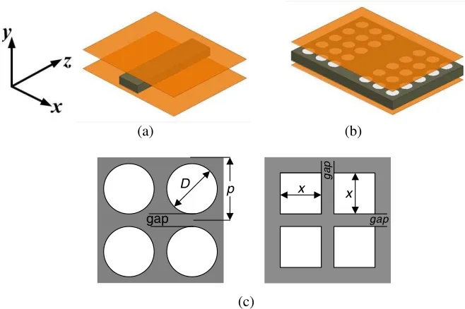
The Non-Radiative Dielectric (NRD) waveguide, shown in Fig. 1, was first proposed in [1, 2] as a low-loss waveguide that has fundamentally addressed the problem of radiation-at-bends-and-discontinuities. This radiation issue has been a well-known shortcoming of its H-guide predecessor [3, 4], which is also an inherent problem for other dielectric waveguides. Therefore, the name “non-radiative” was designated to highlight the physical meaning of this developed dielectric guide. This is simply achieved by ensuring that the operating frequency, fg, is lower than fx; the cut-off frequency of the 1st parallel-plate mode
in the air side-regions (fx=c/2a) [6]. As such, leakage into the side regions belowfx, due to bends and
discontinuities is suppressed [1]. On the other hand, the development of substrate integrated circuits (SICs) suggests that any planar and non-planar structures can be integrated in a hybrid or monolithic manner thanks to the synthesis of non-planar structures in planar form. Designing the NRD guide with the concept of SICs yields the substrate integrated NRD (SINRD) guide [5, 6]. This differs from the NRD guide by the fact that the side regions that flank the guiding channel are made of a lower permittivity dielectric (other than air). This dielectric contrast between the two regions isachieved by perforating the substrate, less the NRD channel width, with non-metalized via holes, as per Fig. 1(a). Some typical perforation profiles are shown in Fig. 1(b) [7]. A perforated region generally has twice the width of the guiding channel to ensure a proper decay of the transverse fields (evanescent waves) in the side regions.
Although the perforation simplifies the physical fabrication of the SINRD guide, it nonetheless limits the application scope of the SINRD guide since the perforated regions are strictly reserved for
Received 19 May 2014, Accepted 4 August 2014, Scheduled 7 December 2014 * Corresponding author: Jawad Attari ([email protected]).
D
gap
p xx x
gap
ga
p
(a) (b)
(c)
Figure 1. (a) The NRD guide and (b) the SINRD guide, and (c) top views of different perforation profiles.
the air via holes. Furthermore, it complicates its theoretical design since any perforation profile will entail additional design parameters that must be accurately identified for operation at a desired fg. Note that any dielectric contrast can be made possible through various techniques such as doping and composite. However, the technique of creating air holes is probably the easiest way to create an SINRD guide without resorting to any sophisticated micro-fabrication process.
In this work, the image approach [8] is applied to the SINRD guide, resulting in the image SINRD (iSINRD) guide, which is half the size of the former, and has significantly wider application potential compared to the SINRD guide. In addition, a simplified design approach is presented, which is applicable to any profile, as compared to the limited discussion in [6], and it takes into account the variation of
fg with εr2 [9], which in [6, 7] is assumed constant. The proposed approach is based on the efficient
Eigen-mode analysis technique discussed in [10] and conducted with the aid of a commercial Eigen-mode solver [11]. The proposed design ideas are validated by designing a set of different iSINRD transmission lines at 94 GHz.
2. THE IMAGE SINRD GUIDE
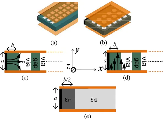
The iSINRD guide is realised by bisection of the SINRD guide with an image PEC wall, as shown in Fig. 2(a). The outcome is that the LSE10 and the TE10 modes are suppressed along with all other
even modes. This leaves the LSM10 mode as the only dominant mode. Although the LSE10 and the TE10 modes are useful for some applications [12–14], the absence of the former solves the well-known
problem of LSM10−LSE10 mode conversion which occurs at bends and corners [15]; while the latter
can be mimicked by theTE20 mode that the iSINRD guide supports. An example of application that
benefits from the absence of theLSE10mode is the iSINRD cruciform coupler reported in [16] while the
planar iSINRD orthomode-transducer reported in [17, 18] is based on the use of the orthogonalLSM10
and TE20 modes. The cut-off of those modes can be obtained in a similar fashion as the conventional
waveguide modeling by matching the Ey components at the air-dielectric interface, leading to the
following equations: LSM10 mode:
β2 =k2
0−(π/a)2−βx2 (1a)
βxtan(βxb/2) = (εr1/εr2)ϕ (1b)
ϕ2 =k2
y
x
z
(a) (b)
(c) (d)
(e)
Figure 2. A schematic 3-D view of iSINRD guide with (a) a square profile and (b) a circular profile, (c) the E-field of the LSM10 mode and (d) theT E20 mode and (e) the perforated region represented
as a dielectric material with a lower permittivity (εr2). Green: Substrate; white: air vias, black: PEC
image plane; orange: metal covers.
TE20 mode:
β2 =κ2
0−βx2 (2a)
βxcot(βxb/2) =ϕ (2b)
ϕ2=k2
0(εr−εr2)−βx2. (2c)
whereβx andϕare, respectively, the propagation and attenuation constants in the guiding channel and the perforated regions.
3. PROPOSED DESIGN APPROACH
The best way of beginning the design procedure of the iSINRD guide is to visualize it as an alternative iSINRD waveguide with the side regions filled with an unknown dielectric material (1 < εr2 < εr1). This simplifies the discussion substantially. The εr2-dielectric is an electrically abstract or equivalent
representation of the perforated regions. Hence, regardless of what the perforation profile is, the designer needs only to look at the resultant or equivalentεr2; hereby reducing the design complexity to only three
variables (a,b, andεr2). Note that this concept of equivalence is only valid for a specific mode, namely
theLSM10 mode in this case. Relatingεr2 to the dimensions of the perforation profile is then left as a
last step, which varies depending on the perforation profile. Fig. 2(c) illustrates a cross-sectional view of this visualisation.
surface waves, and hence a higher dielectric contrast between the dielectric and the surrounding medium correspond to better attenuation of the field in the surrounding; i.e., waves are more confined in the central dielectric [23]. Therefore, Alumina is chosen in the rest of this work. The discussion in the following subsection confirms this choice.
3.1. The Minimum Operating Frequency, fn and the Choice of Thickness a
For any given a,b can theoretically assume any value in the abstract range [0 :∞]. If b= 0, then the structure is a parallel-plate waveguide filled with aεr2-dielectric, whose 1st mode cut-off frequency is
fc1=fx=c/(2a√ε2) (3)
Since this is the maximum operating frequency of operation, then, forb >0, the structure becomes an NRD guide whose fg < fx; a rather obvious result. Now, if b is continuously increased to b = ∞,
then the structure is again a parallel-plate waveguide, filled with a εr1-dielectric material, whose 1st
mode cut-off frequency is
fc2=fn=c/(2a√ε1) (4)
Sincefn can only be obtained forb=∞, and is independent ofεr2, then it is intuitive to conclude
that operation below this frequency is impossible for 0< b <∞. Hence, fnis the “minimum operating
frequency” at which the NRD guide can operate. Since both fx and fn depend on a, each value of a corresponds to a distinct set of fx −fn limits or operating frequency bands (fg-bands), as shown in Fig. 3. Thus, varyinga in the range [0 :∞] results in a super-band of fg-bands. At the lower part of the spectrum, the bands strongly overlap, and the choice ofais no longer critical; i.e., the super-band saturates at lower frequencies. This scenario is reversed at the upper part of the spectrum. Hence, a should be chosen such that it corresponds to an fg-band that covers the desiredfg.
3.2. Determining the Optimum Thickness a
The choice of thicknessashould be such that the desiredfg is not close to eitherfx orfn, as unrealistic values of channel width b would be required (close to zero or infinity). For small increments of a (typically, Δa= 5 mil), the decision should be made based on which band corresponds to the maximum number of εr2 values for the desired fg. This is to ensure design flexibility and robustness. That is, a wider range ofεr2 values gives more flexibility in choosing the perforation profile. This is illustrated in Fig. 3(b).
The above analysis is valid for any dielectric material and for any thickness. In fact, any particular
fg-band can be obtained with different εr1-dielectrics by adjusting their respective thicknesses, a; as
per Fig. 3(c). Obviously, for the same fg-band, higher fx, (and thus fg and bandwidth) values can be
attained with high εr1 dielectrics, since a larger εr2/εr1 contrast ratio can be theoretically conceived
compared to the dielectrics with smallerεr1. This verifies the observation in [24] that highεr1substrates
yield considerably larger bandwidth. Furthermore, compared to low εr1 dielectrics, high εr1 dielectrics
require a smaller thickness “a” to obtain the same fg-band; which is in-line with the miniaturization
trend of RF circuits. In light of the above, the optimum substrate and its thickness, for the W-band, are Alumina anda/λg = 0.635, respectively.
3.3. Determining Channel Width, b and Effective Permittivity εr2
Intuitively, each fg-band should in turn contain operation curves for different values of b, as shown in
Fig. 4(a) for Alumina (εr1 = 9.8) witha/λg = 0.635. Ideally, minimizingεr2 is desired asfx would then
be maximized; but this requires intense perforation and can increase substrate fragility. Conversely, high values of εr2 reflect very little perforation and thus higher susceptibility to leakage. As a compromise,
εr2/εr1 = 0.5. According to Fig. 4(b), this corresponds to b= 0.826λg. In terms of bandwidth (%Δf),
these values correspond to a 16.5% bandwidth, as per Fig. 4(c). The bandwidth is calculated using:
%Δf = [(fx−fc,LSM10)/fg]×100% (5)
(a)
(b)
(c)
Figure 3. (a) Frequency bands for different thicknesses computed with MATLAB, (b) the SINRD guide frequency bands for different values of a, and (c) different dielectrics with unequal thicknesses having the same fg-band.
3.4. Relating εr2 to Perforation Dimensions
(a)
(b)
(c)
Figure 4. (a) Operation curves, within an fg-band, for different values of the width,b, (b) validating the choice of εr2/εr1 and b for the desired fg, (c) and bandwidth corresponding to different ratios of
εr2/εr1 and different values of b.
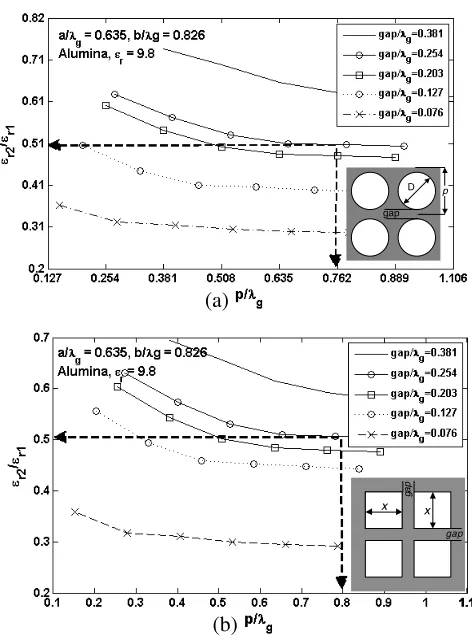
perforation profile models the original NRD/iNRD guide more closely (since the only difference would be the periodic inter-via gaps). Hence, a trade-off is needed that would depend on the target application and/or the performance parameter being investigated. Fig. 5(a) and Fig. 5(b) display the relationship between the ratio εr2/εr1 and the period p of circular-via and square-via unit-cells, respectively, for
(i.e.,p/λg = 0.8) would be needed to obtain the desiredεr2/εr1 = 0.5 ratio.
D
gap
p
x
x x
gap
ga
p
(a)
(b)
Figure 5. (a) Relating εr2/εr1 to p/λg (p=gap+D) for the circular and (b) square via profiles.
To conclude, this section provides an efficient way of choosing the optimum dimensions of the SINRD guide. Specifically, at 94 GHz using Alumina, and circular-via perforation, its dimensions are:
a/λg = 0.635, b/λg = 0.826, D/λg = 0.508, and gap/λg = 0.254, respectively; corresponding to
fc = 84 GHz, andfx= 102.5 GHz. Alternatively, the same performance can be achieved with a square-via perforation that differs from the circular counterpart only in the dimension of the square-square-via. In the case of the iSINRD guide, the width is bi =b/2λg = 0.413. Fig. 6 verifies that the NRD, iSINRD
and SINRD guides are identical, by plotting the dispersion curve of the LSM10 mode, obtained with
the Eigen-mode solver using the equation (whereϕ and Δl are the phase difference and the length of the unit cell):
β= πφ
Δl (6)
The calculated dispersion curve of the NRD guide is also included and is identical to the simulated ones. It was obtained by solving Equation (1) above [25]. Also included in Fig. 6 is the propagation curve for theTE20 mode, obtained by solving the Equation (2) above.
Figure 6. Propagation curves of the T E20 and
LSM10 modes in the iSINRD guide.
Figure 7. The leakage loss in discontinuous-iSINRD guide compared to continuous-discontinuous-iSINRD guide (0 gaps).
(a) (b)
Figure 8. (a) Current distribution of the LSM10 mode in the continuous-wall iSINRD guide and
(b) the discrete-wall iSINRD guide.
that a specific value of balso corresponds to a bandwidth of frequencies, and thus anyb value can well correspond to the desired fg. The optimum value in this context refers to a value of b that results in
a bandwidth centered atfg. A non-optimum value ofbthen corresponds to a bandwidth that includes
fg but is centered at another frequency. This explains the reason behind using the term operating
frequency instead of center frequency.
3.5. Continuous and Discontinuous Walls
It is intriguing to investigate the effect of using a discontinuous metal wall instead of a continuous wall. Such a scenario can be realized with a row of periodic metalized slots. In this case, it is imperative to investigate the leakage loss due to the gaps between the slots, in order to determine the optimum number and spacing between gaps (gs). Indeed, Fig. 7 depicts the effect, on the insertion loss, of varying
the number and dimensions of the gaps; assuming lossless dielectric and conductors. It is interesting to note that the leakage loss due to 1 gap with gs/λg = 0.254 and 2 gaps with gs/λg = 0.127 are identical. If the objective is strictly designing an SINRD guide circuit, then a maximum of two gaps with gs/λg = 0.127 or 1 gap with gs/λg = 0.254 should be used so as to minimize the leakage loss. Conversely, in applications such as leaky wave antennas, more gaps with a larger value of gs might deliberately be used to enhance the radiation pattern. It must be noted that the introduction of gaps does not hinder the propagation of the LSM10 mode because the surface currents on the conducting
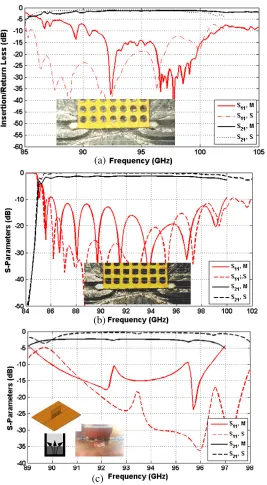
in Fig. 9(a) and Fig. 9(b) along with the simulated S-parameters In both cases, an insertion loss of around 1 dB and a reflection better than 15 dB was obtained. The fabricated prototypes are shown in the insets of Fig. 9(a) and Fig. 9(b).
To demonstrate the versatility of the iSINRD guide, an iSINRD transmission line prototype is
(a)
(b)
(c)
(a)
(b)
Figure 10. (a) The simulated (S) and measured (M) insertion loss and (b) return loss for different gaps.
designed using the method explained in [27, 28] and the PCB technique presented in [25]. In this configuration, the iSINRD guide is fabricated on a RO6002 substrate, and then assembled into a rectangular slot that is machined in a RO6002 substrate, as shown in the upper inset of Fig. 9(c). Here, the feeding is done from a WR10-SIW transition which is explained in [28], which is a much simpler method compared to the WR10 transition used with Alumina. The TE10 mode in the SIW guide is gradually tapered into the iSINRD guide where it converts to theLSM10mode. The simulation
and measured results of this transmission line are shown in Fig. 9(c), while the fabricated line is shown in the lower inset of the same figure. There is a noticeable discrepancy between the simulated and measure response. This is owed to several factors such as the fact that the loss tangent of RO6002 is significantly higher at 94 GHz compared to Alumina. Since the loss tangents of Rogers’ substrates are only available at 10 GHz [22], a significant deviation is expected 94 GHz. This explains the difference between the simulated and measured insertion losses. Furthermore, the solder effects, which are assumed non-existent in the simulation, further impacts the response since it can enter the air-vias that are not shielded (as per the design approach in [25]) as well as between the two substrates. Consequently, additional reflections are anticipated that cannot be accurately gauged. This explains the mismatch between the simulated and measured return losses. Nonetheless, the response is acceptable given the expected lossy nature of the Roger’s substrates at such high frequencies. The drawback in this approach is that it requires very precise assembly alignment and soldering to avoid gaps that would be in the order of the wavelength and can thus easily degrade the performance.
nuisance for NRD circuits involving bends, and its suppression facilitates the use of the iSINRD guide in many novel applications. An alternative and simple methodology for designing general NRD-class guide circuits was also devised and discussed. Specifically, it aids in accurately justifying the choice of dimensions for the guide, as well as the choice of the perforation profile. The advantage of this methodology is that a maximum of only two graphs (Fig. 3(b) and Fig. 4(a) combined, and a graph similar to Fig. 6) is required to determine all the dimensions, even though the iSINRD involves at least
three times the number of parameters of the original NRD guide. Furthermore, if a dielectric of effective permittivity is used instead of air, then only one graph (Fig. 3(b) and Fig. 4(a)) is needed. A number of prototypes were fabricated and tested and the measurements in general are satisfactory.
REFERENCES
1. Yoneyama, T., “Millimeter-wave integrated circuits using nonradiative dielectric waveguide,”
Electronics and Communications in Japan (Part II: Electronics), Vol. 74, No. 2, 20–28, 1991. 2. Koul, S. K., Millimeter Wave and Optical Dielectric Integrated Guides and Circuits, Chapter 6, J.
Wiley & Sons, 1997.
3. Tischer, F. J., “A waveguide structure with low losses,” Archive der Elektrischen Ubertragung, Vol. 7, 592–596, 1953.
4. Tischer, F. J., “H guide with laminated dielectric slab,”IEEE Transactions on Microwave Theory and Techniques, Vol. 18, No. 1, 9–15, 1970.
5. Cassivi, Y. and K. Wu, “Substrate integrated nonradiative dielectric waveguide,” IEEE Microwave and Wireless Components Letters, Vol. 14, No. 3, 89–91, 2004.
6. Cassivi, Y. and K. Wu, “Substrate integrated circuits concept applied to the nonradiative dielectric guide,”IEE Proceedings Microwaves, Antennas and Propagation, 424–433, 2005.
7. Cassivi, Y., “Etude et development de la technologie hybride circuit planaire/guide NRD dans le contexte d’un emetteur/recepteur onde millimetrique,” Ecole Polytechnique de Montreal, 2004. 8. Sugawara, Y., N. Nakaminami, N. Ishiii, and K. Itoh, “A proposal of image NRD waveguide and
radiation from its end,”Trans. IEICE B, Vol. J82-B, No. 4, 637–644, Apr. 1999 (in Japanese). 9. Menzel, W. and J. Al-Attari, “Suspended stripline filters integrated with standard multilayer
printed circuit boards,”German Microwave Conference, 1–4, 2009.
10. Attari, J., T. Djerafi, and K. Wu, “Fast and accurate simulation of novel millimeter-wave circuits based on commercial software package,”IEEE Microwave Magazine, Vol. 14, No. 2, 106–111, 2013. 11. ANSYS and Inc., “Ansys HFSS,” Cannonsburg, PA, 2011.
12. Schmid, U. and W. Menzel, “Planar antenna arrays using a feed network with nonradiative dielectric (NRD) waveguide,” First European Conference on Antennas and Propagation, EuCAP 2006, 1–4, 2006.
13. Schmid, U., W. Menzel, Y. Cassivi, and K. Wu, “Dual polarization antenna fed by a dual mode substrate integrated NRD-guide,” IEEE Antennas and Propagation Society International Symposium, Vol. 4, 4348–4351, 2004.
14. Wong, M., A. R. Sebak, and T. A. Denidni, “Wideband Bezier curve shaped microstrip to H-guide transition,”Electronics Letters, Vol. 45, No. 24, 1250–1252, 2009.
15. Li, D., Y. Cassivi, P. Yang, and K. Wu, “Analysis and design of bridged NRD-guide coupler for millimeter-wave applications,” IEEE Transactions on Microwave Theory and Techniques, Vol. 53, No. 8, 2546–2551, 2005.
17. Attari, J., T. Djerafi, and K. Wu, “Planar othogonal mode transducer based on orthogonalLSM10
and TE10 modal fields of co-layered image SINRD (iSINRD) and SIW guides,” 43rd European Microwave Conference, 597–600, 2013.
18. Attari, J., T. Djerafi, and K. Wu, “A 94 GHz planar orthogonal mode transducer,” International Journal of Wireless and Microwave Technologies, 1–12, Apr. 2014.
19. Balanis, C. A., “Measurements of dielectric constants and loss tangents at E-band using a Fabry-Perot interferometer,” NASA Technical Note, No. NASA TN D-5583, 1969.
20. Bolivar, P. H., M. Brucherseifer, J. G. Rivas, R. Gonzalo, I. Ederra, A. L. Reynolds, M. Holker, and P. de Maagt, “Measurement of the dielectric constant and loss tangent of high dielectric-constant materials at terahertz frequencies,” IEEE Transactions on Microwave Theory and Techniques, Vol. 51, No. 4, 1062–1066, 2003.
21. Afsar, M. N., “Dielectric measurements of millimeter-wave materials,” IEEE Transactions on Microwave Theory and Techniques, Vol. 32, No. 12, 1598–1609, 1984.
22. Corporation, R., “Rogers corporation high frequency materials product selector guide,” Chandler, Arizona, 2011.
23. Patrovsky, A., “Hybrid integration of synthesized dielectric image waveguides in substrate integrated circuit technology and its millimeter wave applications,” Ecole Polytechnique de Montreal, 2008.
24. Koul, S. K., Millimeter Wave and Optical Dielectric Integrated Guides and Circuits, John Wiley & Sons, 1997.
25. Xu, F. and K. Wu, “Substrate integrated nonradiative dielectric waveguide structures directly fabricated on printed circuit boards and metallized dielectric layers,” IEEE Transactions on Microwave Theory and Techniques, Vol. 59, No. 12, 3076–3086, 2011.
26. Moldovan, E., R. G. Bosisio, and K. Wu, “W-band multiport substrate-integrated waveguide circuits,”IEEE Transactions on Microwave Theory and Techniques, Vol. 54, No. 2, 625–632, 2006. 27. Khatib, B. Y. E., T. Djerafi, and K. Wu, “Substrate-integrated waveguide vertical interconnects for 3-D integrated circuits,” IEEE Transactions on Components, Packaging and Manufacturing Technology, Vol. 2, No. 9, 1526, Sep. 2012.
28. Doghri, A., A. Ghiotto, T. Djerafi, and K. Wu, “Compact and low cost substrate integrated waveguide cavity andbandpass filter using surface mount shorting stubs,”International Microwave Symposium Digest, 1–3, 2012.