MANUAL
RESTRICTED' DISTRIBUTION
MARCH 1962
1
CENTRAL PROCESSOR
LOGIC DESCRIPTION
UNIVAC® III
o
y
EM
DIVISION OF SPERRY RAND CORPORATION
-Published by
Section 2
Introduction to 'the UNIVAC III
Logic Components
&
Assemblies;
and a Description of 'the
Cycli.ng Uni't
Under Preparation
Heading 1-l. 1-2. 1-3. 1-4. 1-5. 1-6. 1-7. 1-8. 1-9. 1-10. 1-1l. 1-12. 1-13. 1-14. 1-15. 1-16. 1-17. 1-18. 1-19. 1-20. 1-21. 1-22. 1-23. 1-24. 1-25. 1-26. 1-27. 1-28. 1-29. 1-30. 1-31. 1-32. 1-33. 1-34. 1-35. 1-36. 1-37. 1-38. 1-39. 1-40. 1-41. 1-42. 1-43. 1-44.
CONTENTS
TitleSECTION 1. INTRODUCTION AND GENERAL DESCRIPTION
Central-Processor Specifications .
UNIVAC III Central-Processor Logic Features. Four-bit Parallel Transfer
Overlapping Operation . Multiprecision Instructions Priority
Multiply Instructions
Initiate Input-Output Instruction.
Automatic-Programming Aids . . . . . Scatter-Read/Gather-Write Control Word Number-System Compatibility
Checking Features
Functional Components of Central Processor Computer-Control Register
Instruction -Control Section Storage-Address Section Field-Select Section Memory-Address Section Arithmetic Section
Input-output Control Section Priority Section
Write Register
Sense -Flip-Flop Section . Interrupt Section
Typewriter and Real-Time-Clock Section Cycling- Unit Section and Display Section UNIVAC III Word Formats
Data Words ~ .. Instruction Word
Input-Output Specification Words Control Words
Data Flow in the UNIVAC III Central Processor Data Flow During an Instruction Call
Data Flow when Reading the Instruction from Memory
Data Flow During the First Operand Call Data Flow During the Field Selection and
Indirect Addres sing
Data Flow During Multiprecision Instructions Data Flow I'uring Instructions which use the Main
Adder
Recomplementing
High, Low, and Equal Flip-Flops Extract Instructions
Multiply and Divide Instructions
Store- and Load-Accumulator Instructions Data Flow During Instructions which Transfer Data
Heading 1-45. 1-46. 1-47. 1-48. 1-49. 1-50. 1-51. 1-52. 1-53. 1-54. 1-55. 1-56. 1-57. 1-58. 1-59. 1-60. 1-61. 1-62. 1-63. 3-l. 3-2. 3-3. 3-4. 3-5. 3-6. 3-7. 3-8. 3-9. 3-10. 3-11. 3-12. 3-13. 3-14. 3-15. 3-16. 3-17. 3-18. 3-19. 3-20. 3-21. 3-22. 3-23. 3-24. 3-25. 3-26. 3-27. 3-28. 3-29. 3-30. Title
Data Flow During Instructions which Store the Contents of a Storage-Address Register . • Data Flow During Instructions which Load a
Storage-Address Register
Data Flow During Instructions which Modify and Compare the Contents of an Index Register Data Flow During Shift Instructions
Data Flow During Miscellaneous Instructions Sense-Flip-Flop Instructions
Interrupt Instructions
Data Flow During the Expand Instruction Data Flow During a Compress Instruction Data Flow During Transfer Instructions Data Flow During Zero-Suppress Instruction Data Flow During Typewriter Instructions . Data Flow During Input-output Operations
Data Flow when Transferring the Specification
Word to Memory • •• •
Data Flow when Transferring the Specification Word From the Standby Location
Data Flow for Data Word for All Devices Except Tape Units . • • . • • . . • . • • • Data Flow for Transferring the Scatter-Read/
Gather-Write Control Word
Data Flow for Words During Tape Operations UNIVAC III Instructions
SECTION 3. INSTRUCTION-CONTROL SECTION
Introduction
Instruction Decoder . Program Counter
Accumulator-Register Selector Index-Register Selector
Memory-Request Network Instruction Decoder .
Instruction Register Octal Decoder . Group Encoder
Instruction-Line Generator. Program Counter
General Operation
Program-Counter Cycles . Normal Cycle
Shift Cycle
Recomplement Cycle Multiply Cycle Divide Cycle
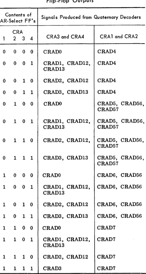
Accumulator-Register Selector AR-Select Flip-Flops . AR-Decode Network AR-Selection Network
Function Signals 235, 236, 237, and 238 Function Signal 1 2 8 . •
Function Signal 129
Selection of Accumulator Registers Precision Selection
Other Selection Functions of the AR-Select Flip-Flops
Index-Register Selector •
Heading 3-31. 3-32. 3-33. 3-34. 3-35. 3-36. 3-37. 3-3S. 3-39. 3-40. 3-41. 3-42. 4-1. 4-2. 4-3. 4-4. 4-5. 4-6. 4-7. 4-S. 4-9. 4-10. 5-1. 5-2. 5-3. 5-4. 5-5. 5-6. 5-7. 5-S. 5-9. 5-10. 5-11. 5-12. 5-13. 5-14. 5-15. 5-16. 6-1. 6-2. 6-3. 6-4. 6-5. 6-6. 6-7. Title
Instruction Memory Requests Instruction-Control Signal Multiprecision Instructions Zero-Suppress Instruction Shift Instructions
..
.
.
.
Error ConditionsOperand Memory Requests Instruction-Control Signals
The CVEP Signal The CVRINH Signal The CVRE CP Signal The CCVA Signal
.
.
SECTION 4. PRIORITY SECTION
Introduction . . . . Priority Order . . . . Operation of Priority Channels .
Operation of Central-Processor Channels Automatic Operand Call
Transfer Instructions A utomatic Interrupt Multioperand Calls . . Priority Inhibits
Priority Manual Reset
SECTION 5. COMPUTER-CONTROL REGISTER
Introduction . . . . General Operation . . . • • . . • . • Logic of Computer-Control Register.
Register Functions • • . . . . Resetting • • . . . . • • • • •
Jamming Binary Zeros . • . • • . . • . . . . • . Decimal Shifting and Circular-Decimal
Shifting • . . . • . • . • • . . • . . Binary Shifting and Circular-Binary Shifting.
Register Inputs . . • • . . . • • .
Memory Input . . . Typewriter Input
Real-Time-Clock Input . . . . • • . Interrupt Inputs . . • • .
Accumulator-Register Inputs
Synchronizer-Control-Register Inputs Register Outputs . • • . . . • • . . • • .
SECTION 6. STORAGE-ADDRESS SECTION
Introduction . . . • . . . • • Selection of SAr's and TCWr's Inputs to SAr's and TCWr's Outputs from SAr's and TCWr's Logic of the SAr and T CWr Selection
Selection of SAr' s . . . • . . . Selection of Index-Register ••
Heading
6-8. 6-9. 6-10.
7-1. 7-2.
7-3.
7-4. 7-5. 7-6. 7-7. 7-8.
7-9.
7-10.
7-11. 7-12.
7-13.
7-14. 7-15. 7-16. 7-17. 7-18.
8-1. 8-2.
8-3.
8-4. 8-5. 8-6. 8-7.
8-8.
8-9.
Title
Selection of Memory-Address Counters Selection of TCWrv s . • • • • • • • • . •
SAr and TCWr Outputs . . . • . • . • . .
SECTION 7. MEMORY-ADDRESS SECTION Introduction . . . • .
Memory Adder . . . Subtrahend Inputs Minuend Inputs ••
CMAC Pulseformer Inputs . . . • . Memory-Adder Addition Logic .
Memory-Address Parity Generator • • . • . . • . . • • Generation of Parity Bit From the Memory-Adder
Output . • . . . • • • • • • . • • • • • . • • • • • Generation of Parity Bit During SAr or
Store-TCWr Instructions . . . • . . • . . . . Generation of Parity Bit During Initiate 1-0
Instruction . . . . . . • • • . Modulo-3 Check-Bit Generation . . . . • . . Memory-Address Selector . . . . • . • . . .
Memory-Address Selector Operation Memory-Address Selector Inputs . • Memory-Cabinet Selector
Zero-Detector Flip-Flop T ape Operation . . . The 53 Instruction
SECTION 8. MEMORY-WRITE REGISTER Introduction . • . . . . • •
Central-Processor Format . • Accumulator Register. . Memory Adder . . . . UNISERVO III Format
Input-output Format . . . . . . . Computer-Control-Registel' Format, Expand Instruction
Only. . . . . . . Maintenance-Panel Format . .
Summary of Functions
Page
6-4
6-6 6-8
7-1 7-2 7-2
7-3
7-5 7-6 7-8
7-8
7-10
7-10 7-10 7-12 7-12 7-12 7-15 7-16 7-16 7-16
8-1 8-1 8-1 8-2 8-2 8-4
8-7 8-9 8-9
APPENDIX A. ENGINEERING-DRAWING SOURCES OF ILLUSTRATIONS
Figure
1-1. 1-2.
ILLUSTRATIONS
Title
Central Processor, Functional Block Diagram Data Flow During an Instruction Call,
Functional Block Diagram . . . .
Page
1-5
Figure 1-3. 1-4. 1-5. 1-6. 1-7. 1-8. 1-9. 1-10. 1-11. 1-12. 1-13. 1-14. 1-15. 3-1. 3-2. 3-3. 3-4. 3-5. 3-6. 3-7. 3-8. 3-9. 3-10. 3-11. 4-1. 4-2. 4-3. 5-1. 5-2. 5-3. 5-4. Title
Data Flow During Multiprecision Instructions, Functional Block Diagram
Data Flow During Instructions Which Use the Main Adder, Functional Block Diagram
Example of Double-Precision Add with Carries, Functional Block Diagram
Loading Accumulator Registers from Adjacent Memory
Locations, Diagram •
Storing Contents of Accumulator into Adjacent Memory Locations, Diagram
Data Flow During Storage-Address-Register Load and Store Instructions, Functional Block Diagram • Data Flow During Index-Register Modify and Compare
Instructions, Functional Block Diagram
Shifting Right with Right Shifts or with Left Shifts, Diagram Data Flow During Double-Precision Two-Digit Right Shift,
D i a g r a m . • •
Data Flow During Double-Precision Two-Digit Left Shift,
Diagram • •• • • • • • • • • • ••
Data Flow During Typewriter Interrupt, and Sense-Flip-Flop Instructions, Functional Block Diagram. • Data Flow During Expand and Compress Instructions,
Functional Block Diagram • • • • •
Data Flow During Input-Output Operations, Functional
Block Diagram • • • • • •
Instruction-Control Section, Functional Block Diagram
Instruction Register and Octal Decoder, Detailed Block Diagram ..
Program Counter, Detailed Block Diagram Timing Diagram for Typical Program Cycles AR-Select FF's and Decode Network, Detailed
Block Diagram
Production of Function Signals 235, 236, 237, and 238, Detailed Block Diagram
Production of Precision Signals, Detailed Block Diagram
Index-Register Selector, Detailed Block Diagram Production of the CVEP Signal, Detailed
Block Diagram and Timing Diagram Production of the CVRINH Signal, Detailed
Block Diagram and Timing Diagram Production of the CCVA Signal, Detailed
Block Diagram and Timing Diagram Typical Priority Channel, Detailed Block
Diagram
Automatic Operand Call, Detailed Block Diagram
Transfer Instructions, Detailed Block Diagram
Computer-Control Register, Functional Block Diagram
Example of the Transfer of a Word from Memory Through the Computer-Control Register to Main Adder, Functional Block Diagram Decimal Shift, Circular-Decimal Shift,
Binary-Zero Entries into the Computer-Control Register, Detailed Block Diagram
Binary Shift, Circular-Binary Shift, and Jammed Zeros into the Computer-Control Register, Detailed Block Diagram
Figure
5-5.
5-6.
5-7.
6-1.
6-2.
6-3.
6-4.
7-1.
7-2.
7-3.
7-4.
7-5.
7-6.
7-7.
7-8.
7-9. 7-10. 7-11. 8-1.
8-2.
8-3.
8-4.
8-5.
8-6.
8-7.
8-8.
8-9.
8-10.
Title
Parallel Inputs from Memory, Real-Time Clock, and Typewriter into the Computer-Control Register, Detailed Block Diagram
Accumulator Register Loading Computer-Control Register and XS-3 Zeros Entered During Multiply and Divide, Detailed Block Diagram. Synchronizer-Control Register Loading the
Computer-Control Register, Detailed Block Diagram
Storage-Address Section, Functional Block Diagram
Storage-Address-Register and Tape-Control-Word-Register Selection, Detailed Block Diagram
Production of Storage-Address-Register and Tape-Control-Word-Register Function Signals, Detailed Block Diagram
Production of Function Signals 222 through 234, Detailed Block Diagram
Memory-Address Section, Functional Block Diagram
Production of Memory-Adder Subtrahend Inputs, Detailed Block Diagram
Production of Memory-Adder Minuend Inputs, De-tailed Block Diagram
Production of Function Signal 104, Detailed Block Diagram
Production of Add-1 (CMAC) and Add-2 (Function Signal 212) Signals, Detailed Block Diagram Memory-Adder Parity-Bit Generation, Detailed
Block Diagram
Modulo-3 Check-Bit Generation, Detailed Block
Diagram • •
Memory-Address Selector, Functional Block Diagram
Memory-Address Selector, Detailed Block Diagram Cabinet Selector, Detailed Block Diagram •
Zero Detector, Detailed Block Diagram Memory-Write Register, Functional Block
Diagram • •
Memory-Write Register Loading from the Accumu-lator Registers, Detailed Block Diagram
Production of CVRW1 and Function Signals 121, 270, and 271, Detailed Block Diagram • Memory-Write Register Loading from the Memory
Adder, Detailed Block Diagram
Memory-Write Register Loading from the UNISERVO III Channels, Detailed Block
Dia-gram • ••
Production of Function Signals 131, 148, and 149, Detailed Block Diagram
Memory-Write Register Loading from UNISERVO II and General-Purpose Channels, Detailed Block Diagram
Production of Function Signals 130, 132 through 139, Detailed Block Diagram . Memory-Write Register Loading from the
Computer-Control Register During Expand In-struction, Detailed Block Diagram • • '. • • • .. Production of Function Signals 277, 278, and
280, and the CMW26EJ and CMW27EJ Signals, Detailed Block Diagram
Page
5-7
5-9
5-10
6-1
6-3
6-5
6-7
7-1
7-3
7-4
7-6
7-7
7-9
7-11
7-13 7-14 7-15 7-16
8-2
8-3
8-4
8-5
8-6
8-7
8-8
8-9
8-11
Table
1-1. 1-2.
3-1.
3-2.
3-3.
3-4.
4-1. 5-1.
5-2.
5-3.
5-4.
6-1.
6-2.
6-3. 7-1.
7-2.
7-3.
7-4.
7-5. 7-6. 8-1.
8-2.
8-3.
A-I.
A-2.
A-3.
A-4.
A-5.
A-6.
A-7.
TABLES
Title
UNIV A C III Instructions . . . • . . • . . Sense-Flip-Flop Instruction Designations Decoding of AR-Select Flip-Flop Outputs Selection of Accumulator Registers During
o
8-Type Instructions by Function Signals235 through 238 . . . • . • • • • • . • . • • • • • . • • • Selection of Accumulator Registers During
o
9-Type Instructions by Function Signals 235 through 238 . . . • . . . . • . . • . Precision Signals for All Bit Combinationsin the AR-Select Flip-Flops
Order of Priority Channel . . • . . . . • • . Interrupt Instruction Words . • • . . • . • • • • . Computer-Control-Register Outputs
Summary of Function Signals, Which Control Transfer Operations to and Within Computer-Control-Register Flip-Flops, and Interrupt Inputs . • . • . • . • • . • • . • • . • • • • • Summary of Input Sources and Word Formation • Input and Output Timing of Memory-Address
Counter, Index Register, Tape-Control-Word Register . . • . . . • . • • . • • . • . Production of Function Signal 222 by CSG03 ••• Tape-Control-Word-Register Input Information . Production of the Final Sum and Partial Carry
for the First Bit Position • . . • . . • . . . Production of Partial Sums and Partial Carries
for Bit Positions 2 through 4 • . . • • • • • • Production of Final Sum Bits of 1 for Bit Posi
-tions 2 through 4 • • • • • • • • • • • • • • •
Parity Bit Production From First Gating
Net-work . . . .
Production of Final Parity Bit . • • • • • • • • • Summary of Modulo-3 Check-Bit Generation Memory-Write-Register Inputs from UNISERVO II
and General-Purpose Channels, and Function Signals'. • • • • • • • • • • • • • • • • • • • • Summary of Function Signals Which Enter and
Gate Inputs in the Memory-Write Register Bit-Entry Sequence of Input Formats into
Memory-Write Register • • • • • • • • • . • Figure References and Engineering Drawings
for Section 2 • • • • • • • • • • • • • • • • Figure References and Engineering Drawings
for Section 3 • • • • • • • • • • • • • • • • • • • • • • • • Figure References and Engineering Drawings
for Section 4 • . • • • • • • • • • • • • • . Figure References and Engineering Drawings for Section 5 • . . • • • • • • • • • • • • • Figure References and Engineering Drawings
for Section 6 • • • • • • • • • . • • • • • • • Figure References and Engineering Drawings
for Section 7 • . . . • • • • • • • • • • • • Figure References and Engineering Drawings for Section 8 • . . • . . • • • • • • • • . . .
Page
1-21 1-24 3-10
3-12
3-12
3-13 4-1 5-8 5-11
5-11 5-12
6-2
6-6 6-8
7-8
7-8
7-8
7-9 7-10
7-12
8-4
8-9
8-10
A-I
A-I
A-I
A-I
A-2
A-2
Section 1
INTRODUCTION AND GENERAL DESCRIPTION
This manual describes the logical operation of the UNIVAC ® III Central Processor Model 121. No at-tempt is made to explain in complete detail the in-terrelation of all logic components as shown on the logic diagrams. It is assumed that the reader will be able to determine the details of the central-processor operations from the logic diagrams. In order to aid in the transition from the manual to the logic diagrams, all signal designations men-tioned in the manual are presented in the same form that they appear on the logic diagrams, and appendix A lists all logic prints and the print revisions on which the information in the manual is based.
The related manuals in the UNIVAC III manual se-ries are as follows:
Manual 2, Synchronizers for Peripheral Equip-ment - Logic Description
Manual 3, Logic Diagrams
Manual 4, Signal Analysis
Manual 5, Circuitry
Manual 7, Core Storage Model 122 and Model 197 - Description and Maintenance
Section 1 of manual 1 describes, in general, the major logic areas of the central processor, and section 2 describes all UNIVAC III system logic elements and assemblies. Sections 3 through 14 describe, in detail, the operation of each logic area that was introduced in section 1. The organization of the manual is planned so that the reader may, after reading sections 1 and 2, proceed to any of the twelve sections (sections 3 through 14) without the necessity of reading all sections in sequence.
Sections 1 through 8 contain the introduction to the manual and an explanation of the logic necessary
to read and index instructions. Sections 9 through 14 describe the logic necessary to execute the central-processor instructions.
1-1. CENTRAL-PROCESSOR SPECIFICATIONS
The central processor performs all the data-proc-eSSing functions of the UNIVAC III computing system and coordinates the operations of all input-output devices in the system. The design methods that were so successfully used in the production and maintenance of the LARC* and other UNIVAC solid-state computing systems have been applied to the UNIVAC III central processor. Because of this ex-perience, the UNIVAC III central processor offers features in a medium priced computing system that are normally found only in higher priced systems.
The general, programming, arithmetic, and storage specifications for the UNIVAC III central processor are as follows:
General
Synchronous operation 4 jJ.sec per minor cycle 9 pulse times per minor
cycle Serial-parallel
trans-fer
27-bit words 24 data bits, 1 sign bit, 2 check bits
Typewriter input and output
15 index registers
Automatic sequencing of memory accesses between central proc-essor and input-output units
The following registered trademark of the Sperry Rand Corporation is used in this manual: UNIVAC.
Central Processor Logic
Prograolming
Single- address instructions
Stored program
61 well defined in-structions in SAL T code
8 programmable sense FF's
Automatic interrupt
Autornatic field selection
Indirect addressing
Arithmetic
Operands
Arithlnetic operations performed with either binary or decimal numbers
Storage
Expandable magnetic-core memory
Tested by the program
6,12, 18, or 24 decimal digits
24, 48, 72, or 96 binary digits
4, 8, 12, or 16 alpha-numeric characters
8192, 16,384, 24,576, or 32,768 words
1-2. UNIVAC III CENTRAL-PROCESSOR LOGIC FEATURES
Some of the outstanding features of the UNlV AC III central processor are: 4-bit paralleltransfer, over-lapping operation, multiprecision instructions, pri-ority, multiply instructions, initiate input-output instructions, automatic programming aids, scatter-read/gather-write control, number-system compa-tibility, and checking features.
1- 3. Fo u r-bit Pa rail el Tra nsfer
All data format manipulation in the UNIVAC III central processor is performed four bits (a decimal digit) at a time, and all information is transferred within the central processor four bits at a time. The use of the decimal-digit-at-a-time transfer repre-sents the most efficient way of handling data in a
medium priced decimal computer because the deci-mal digit is the sdeci-mallest unit of information that is normally required.
1-4. Overlapping Operation
The reading of an instruction from memory and the indexing of the instruction is performed whillB the previous instruction is being executed. This over-lapping of instructions is normally found only in the most expensive data processing systems.
1- 5. Mu Iti precis io n I nstructio ns
The UNlV AC III instruction catalogue permits the programmer to designate the precision of the a,rith-metic operation that is to be performed. This pre-sents two distinct advantages: one, the prograrnmer can work directly with numbers that contain as many as 24 decimal digits or 96 binary digits withou.t any programming manipulation; two, an arithmetic op-eration takes only as long to perform as is neces sary . No time is wasted adding meaningless digits when they are not required by the operation. Thus, the greater precision of the long word is combined! with the faster operation and economy of the short word.
1-6. Priority
The UNIV AC III central processor automabcally allots memory access to the central processor and to the input-output (I-O) devices in a way that Dlakes best use of computer operating time. This is a. fea-ture that is normally found only in the most expen-sive computing systems.
1-7. Multiply Instructions
The multiply instruction uses a special techmque called short cut multiply which decreases by one-third the maximum number of additions nece:3sary for a multiply problem.
1-8. Initiate Input-Output Instruction
The instruction which initiates the input-output op-erations, supplies the designated input-output syn-chronizer with all necessary control information, and then transfers control of the input-output oper-ation to the synchronizer. After the initiate 1-0
1-9. Automatic-Programming Aids
Automatic field selection and indirect addressingf
which are invaluable aids in data processing appli-cations, are built into the central processor. Also f
the extensive use of the sense flip-flop and auto-matic-interrupt features provide the programmer and the operator with maximum control over the system.
1-10. Scatter-Read/Gather-Write Control Word
The use of the scatter-read/gather-write control word allows one central-processor instruction to control the transfer of data between magnetic tape and various segments of memory. This transfer is done by the automatic reading of sequential scatter-read/gather-write control words from memory. These control words contain the address of the first memory location of a memory segment and the num-ber of words in that segment. When the data from one segment are processed, the next scatter-read/ gather-write control word is automatically read from memory. Thus, information can be transferred between a tape unit and various segments of memory with one central-processor instruction. This repre-sents a great saving in program time.
1-11. Number-System Compatibility
The central processor performs arithmetic opera-tions with either binary or decimal numbers.
1-12. Checking Features
All transfers between the central processor and memory are checked both for correct transfer and for address decoding. Also, all addition and subtrac-tion operasubtrac-tions are automatically checked.
1-13. FUNCTIONAL COMPONENTS OF CENTRAL PROCESSOR
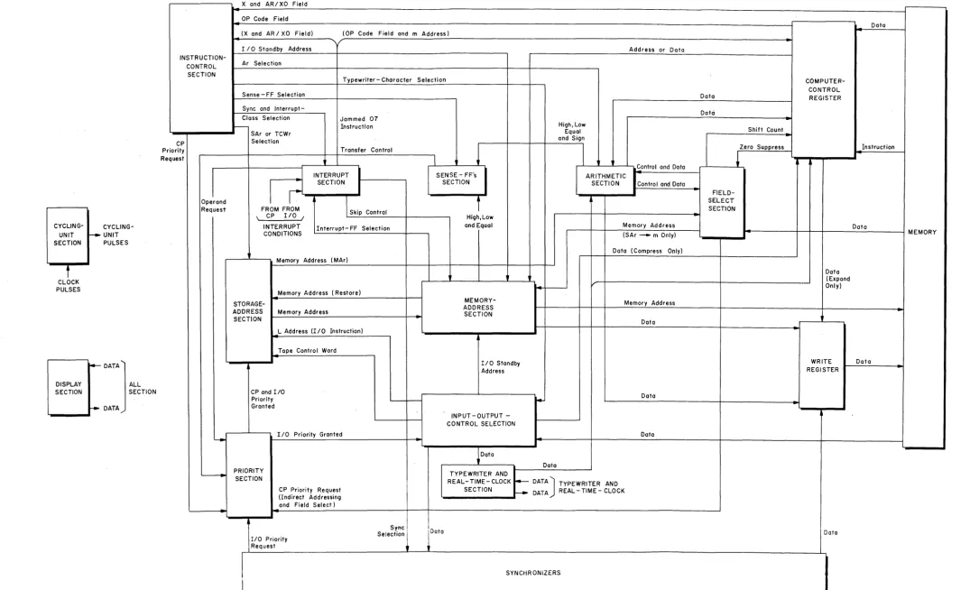
Figure 1-1 shows the functional components of the central processor and the major data-flow paths between these components. The purpose of each functional component will be explained in the text that follows; the data flow will be explained later in this section (heading 1-32).
1-14. Computer-Control Register
The computer-control register (CCr) is the main working register in the central processor. This reg-ister performs all the shifting and data manipulation
Introduction and General Description
that is required by the central processor. The CCr also receives all the memory inputs which contain central-processor data or instructions.
1-15. Instruction-Control Section
The instruction - control section receives each central-processor instruction, partly from memory and partly from the CCr, and then decodes these instructions into various instruction lines, program counts, and register selection outputs as specified by the instruction. These signals then are used by other sections of the central processor to control the execution of the instruction.
1-16. Storage-Address Section
The storage-address section contains a maximum of 30 storage-address registers (SAr). These reg-isters include a maximum of 15 index regreg-isters (Ir) which are used to modify the instruction address; and a maximum of 15-memory-address counters (MAC), which contain input-output memory ad-dresses, an instruction memory address, and an operand memory address. The MAC that contains the instruction memory address is called the control counter (CC), and it stores the address of the last instruction that was read from memory. The ad-dress of the last operand that was read from memory is stored in the MAC called the memory-address register (MAr). All other MAC's contain memory-address information for input-output operations. There is one MAC for each input-output operation and one MAC for each input-output channel.
The MAC's and Ir's contain 15 bits each; corre-spondingly numbered MAC's and Ir' s occupy one 36-bit register (6 bits of this register are not used).
In addition to the storage-address registers, the storage-address section also contains four 24-bit tape-control-word registers (TCWr) which hold con-trol and address information for tape operations, and which occupy one 36-bit register each.
1-17. Field-Select Section
The field-select section, which contains 10 flip-flops and control logic, performs the follOwing functions in the central processor:
Provides signals that control field selection or indirect addressing;
Centra' Processor Logic
Provides temporary storage of arithmetic-carry information during multiprecision operations;
Provides a means of deleting zeros and commas during zero-suppress operations;
Stores and modifies the shift count; and
Provides a means of shifting during multiply and divide operations.
1-18. Memory-Address Section
The address section performs all memory-address rnodification and supplies memory-addresses to mem-ory for both read and write operations. The section contains an adder and a register. The adder, called the memory adder, performs all address modifica-tion, provides a transfer path for storing data during certain instructions, and provides a means of com-paring data during other instructions. The register, called the memory-address selector (MAS), con-verts the address format from serial to parallel, supplies an address to memory, and provides a path for loading either the SAr's or the TCWr's.
1-19. Arithmetic Section
The arithmetic section performs all the arithmetic operations and the data modification for the central processor and provides temporary storage for in-formation. The arithmetic section contains four accumulator registers (Ar! through Ar4) and an adder (called the main adder)" The accumulator reg-isters are addressed either singly or in combination. When addressed, they supply one word at a time to either the write register for storage into memory, or to the computer-control register for data manip-upation, or to the main adder for modification.
When more than one Ar is addressed, the register designated by the smaller number contains the most Significant digits, and the register designated by the larger number contains the least significant digits. For example, if Ar! and Ar4 are designated, Ar! contains the most Significant digits, and Ar4 con-tains the least Significant digits.
The main adder performs the addition process for all arithnletic instructions. Besides its function in the arithmetic instructions, the main adder is used in logical operation instructions (erase and super-impose), is used in comparison instructions, and is the only input path to the Ar's. In all these uses the main adder performs the addition process; the different results are achieved by varying the inputs to the adder.
1-20. Input-Output Control Section
The input-output control section coordinates data transfer between memory and the synchroni.~~ers,
and checks all data transfers between memory and the central processor. The section contains one register, the synchronizer-control register (SCr), which provides temporary storage for all informa-tion that is read from memory. Control logic in the section checks data transfers, arranges data in the SCr into the input-output formats, and coordinates the input-output operations.
1-21. Priority Section
The priority section receives memory requests from the central processor and from the various input-output synchronizers and allots memory acceSB ac-cording to a predetermined sequence. The outputs from the priority section control the reading; and restoring of memory addresses in the storage-address section. The priority-section outputs. are also encoded to produce an address during input-output operations.
1-22. Write Register
The write register supplies data to memory during all store operations. The register receives dB~ta in different formats from the arithmetic section, the synchronizers, the memory-address section, and the computer-control register. The write register then arranges these formats into the memory format and supplies the data to memory.
1-23. Sense-Flip-Flop Section
The sense-FF section contains eight sense FF'13 and an inhibit-input-output-interrupt FF, all of which are set, reset, or tested by an instruction; and three comparison FF's, which represent equal to, greater than, or less than conditions. The appropriate high, low, or equal flip-flop is set during specific instruc-tions if the minuend input is either equal to, greater than, or less than the subtrahend input. The oom-parisons are made either in the memory adder or the main adder. All the flip-flops in the senst~-FF
section can be tested by an instruction. If the flip-flop is set when tested, program control is trans-ferred to a subroutine.
1-~4. I nterru pt Sectio n
CYCLlNG-UNIT SECTION
CLOCK PULSES
DISPLAY SECTION
CYCLlNG-UNIT PULSES
DATA]
DATA ALL SECTION
INSTRUCTION-CP riority
P
Re quest
CONTROL SECTION
Operond Request
L..-.
~
...
X and AR/XO Field OP Code Field
(X and AR I XO Field) (OP Code Field and m Address)
... /
rio
Standby Address Address or DataAr Selection
Typewriter - Character Selection Sense - FF Selection
Sync and
Interrupt-Class Selection Jammed 07
~ Instruction High, Low
SAr or TCWr Equal
Selection and Sign
I
Transfer Control
I
Control and DotoINTERRUPT SENSE- FF's ARITHMETIC
I
SECTION SECTION SECTION Control ond Doto
~
Skipi
FROM FROM
CP IIO ( Control High,Low
\
INTERRUPT Interrupt- FF Selection ond Equal Memory Address
CONDITIONS (SAr - m Only)
Data (Compress Only) Memory Address (MAr)
Memory Address (Restore)
STORAGE- MEMORY- Memory Address
ADDRESS Memory Address ADDRESS
--
SECTIONSECTION Doto
L Add ress (I 10 Instruction)
Tope Control Word
I/O Stondby Address CP and I/O
Data
Priority
I--Granted
INPUTOUTPUT -CONTROL SELECTION 110 Priority Gronted
--
DataData
Data
PRIORITY TYPEWRITER AND
SECTION REAL-TIME-CLOCK
I-- DATA
J
TYPEWRITER AND CP Priority Request SECTIONr--
DATA REAL-TIME - CLOCK (Indirect Addressingond Field Select)
Sync
jD"'"
Se lection I/O Priority
Request
SVNCHR ONlZERS
Introduction and General Description
Data
~
COMPUTER-CONTROL
Data REGISTER
Datci
...
Shift Count
Zero Suppress Instruction
j
FIELD-SELECT SECTION
Data
-
MEMORYDoto (Expand Only)
-WRITE Dota REGISTER
Data
6e47
Central Processor Logic
a transfer instruction is jammed into the eCr and into the instruction-control section. This instruction is then executed.
1-25. Typewriter and Real- Time-Clock Section
The typewriter and real-time·-clock section controls all data transfers between the central processor and either the typewriter or the real-time clock. The section contains a 6-bit buffer register which stores one character at a time; a translator, which trans-lates the 6-bit character into typewriter code; and control logic.
1-26. Cycling-Unit Section and Display Section
The cycling unit supplies all sections of the central processor with timing signals. These signals are produced and controlled by the central clock. The display section contains control logic which lights the indicators on the engineer's console and which permits the manual control of computer operations from the engineer's console.
1-27. UNIVAC III WORD FORMATS
There are four types of word formats used in the UNIVAC III central processor. These types are as follows:
Data words, which represent three types of data;
Instruction words, which represent all instructions;
Input-output specification words, which control the operation of the input-output devices; and
Control words, which perform special functions during specific instructions.
All word formats contain check bits in bit-positions 26 and 27. These check bits are not included in the descriptions that follow.
1-28. Data Words
There are three types of data words: the decimal data word, the alphanumeric data word, and the binary data word.
The format of the decimal data word is as follows:
25 24
IS I
DIGIT6~
____ - L _ _ _ _~
_ _ • _ _ _ _ _~
_ _ _ _~
___ _ _where
DIGIT (1 through 6) represents six decimal digits
in XS-3 code. .
S represents the sign bit (0 for positive, 1 for negative).
The format of the alphanumeric data word j,s as follows:
25 24 1918 1312 7 6 1
Is I
CHARC 4I
CHARC 3I
CHARC 2I
CHARI~
where
CHARC (1 through 4) represents four alpha-numeric characters.
S is the same as in the decimal data word.
The format of the binary data word is as follows:
25 24 1
l~s~1
__________________
B_I_NA_R_Y ___ N_U_M_B_E_R _____________~
where
BINARY NUMBER represents one 24-bit binary number.
S is the same as in the decimal data word.
1-29. Instruction Word
There is one general instruction word which is used for all instructions.
The format of the instruction word is as follows.:
25 24 21 20 1514
x
I
OP CODEI
where
AR
-
XO1110 1
m ADDRESS
~
AR/XO represents the following:
The precision of an arithmetic operation, and the Ar's specified in instructions that use Ar's;
The sense FF that is to be addressed during a sense- FF instruction;
The SAr designated during an SAr-load or -store instruction;
The TCWr that is specified during a TCWr-store instruction;
rhe type of interrupt FF specified during a test, or reset interrupt- FF instruction; or
The synchronizer and standby location to be used during an initiate I-a instruction.
OP CODE is the octal representation of the instruc-tion to be performed. X represents the index reg-ister which modified the m-ADDRESS field. IA/FS represents the indirect-addressing or field-selec-tion control bit.
1- 30. I n put -0 u t put 5 p e ci fi cat ion W 0 r d s
Bit positions 1 through 15 of the input-output speci-fication word contain the L address which is the ad-dress of the first data word, and bit positions 17 through 24 contain information which controls the operation of the synchronizer. The specific function performed by the contents of bit positions 17 through 24 varies with each input-output unit and these func-tions are described in the synchronizer manuals.
Bit position 16 of the I-a specification word causes a program interrupt if it contains a I-bit.
1-31. Control Words
The four types of control words are as follows:
Indirect-addressing control word, which specifies the addres s of the next operand during indirect addressing;
Field-selection control word, which specifies the address of an operand and selects a specified field within that operand;
Index-register-modification control word, which specifies the number with which an index register is to be modified and compared; and
Scatter-read/ gather-write control word, which specifies the address of the first data word and
Introduction and General Description
the number of words to be transferred during a tape operation.
The format of the indirect-addressing control word is as follows:
25 24 21 20 1817 1615
L ADDRESS
where
L ADDRESS represents the address of the next operand. (This address is indexable.)
Bits 18 through 20 must be all O's.
X represents the index register which modifies the L ADDRESS field.
IA/FS represents the field-selection or indirect-addreSSing control bit.
The format for the field- selection control word is as follows:
25 24 2120 1615 1110
x
I
LBBRBB
m ADDRESSwhere
m ADDRESS represents the least Significant 10 bits (unmodified) of the next operand address.
RBB (right-boundary bit) represents the bit posi-tion of the least-significant bit (LSB) of the field that is selected.
LBB (left-boundary bit) represents the bit position of the most-significant bit (MSB) of the field that is selected.
X represents the index register which modifies the m address.
Bit 25 must be a O.
The format for the index-register-modification con-trol word is as follows:
25 24 109
CA MA
Central Processor Logic
MA represents the amount by which the index reg-ister is modified (increased or decreased).
CA represents the number with which the modified index register is compared.
(*If bit position 25 contains a 0, the contents of the MA··field is added to the contents of the Ir; if bit position 25 contains a 1, the MA-field is sub-tracted.)
The format for the scatter-read/ gather-write control word is as follows:
2524 1615 1
1*1
~_O_UN_T
____
~I
_______
L
__
AD_D_R_E_S __
S ______
J
where
L ADDRESS represents the address of the first data word. (This address is not indexable.)
COUNT represents the number of words to be processed.
(*If bit 25 is aI, it means that this is the last scatter-read/gather-writer control word, and bits 1 through 24 are ignored.)
1-32. DATA FLOW IN THE UNIVAC III CENTRAL PROCESSOR
The major data flow in the central processor is as follows:
Data flow during an instruetion call (when an in-struction is read from memory);
Data flow during multiprecision instructions:
Data flow during instructions which use the ma1.n adder;
Data flow during instructions which transfer data between the SAr and memory;
Data flow during shift instructions;
Data flow during miscellaneous instructions such as transfers, sense- FF instructions, expand in-structions, and zero-suppress instructions; and
Data flow during the input-output operations.
1-33. Data Flow During an Instruction Call
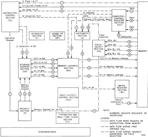
The data flow during an instruction call (figure 1-2) is divided into three parts: the reading of the
in-struction from memory; the reading of the first op-erand from memory, called the first opop-erand call; and the performance of field selection or indlrect addressing. The first two parts are performed for all instructions, and the third part is performed only when specified by a 1 in the 25th bit position of the instruction word.
1-34. DATA FLOW WHEN READING THE INSTHUC-TION FROM MEMORY. A memory request for an instruction is produced at the end of the previous instruction by the instruction-control section. The request is routed to the priority section where rnem-ory access is granted. When memrnem-ory acceBS is granted, the contents of the CC (in the storage-address section) are transferred to the adder in the memory-address section where they are increased by 1. The contents of the CC-plus-l are then sent to the memory-address selector, and from there to memory. The location specified by the contents of CC-plus-l contains the next instruction. When the instruction is read from memory, the X- and AR/ XO-fields are read directly into the instruction-control section and the complete instruction word is read into the CCr.
1-35. DATA FLOW DURING THE FIRST OPERAND CALL. The contents of the X- and AR/XO-fields are decoded by the instruction-control section" The X-field selects an index register and the AR/XO-field selects an accumulator register. The contents of the selected Ir and the m address from the CCr then are added in the memory adder. At this time, the operation code is read from the CCr to the instruction-control section. As a result of this de-coding process, the index-register and accumulator-register selections are made before the operation code is decoded.
The m' address is sent to the MAS and, from there, to memory and to MAr. Also, the contents of the specified Ar are sent to the write register at this time. If the instruction is a store instruction, the contents of the write register are written into Dlem-ory. Otherwise, the contents of the memory location specified by the m' address are read into the CCr. Many instructions do not require an operand. In
these cases, the CCr is cleared during the next minor cycle.
The 25th-bit position of the instruction is transferred into the field-select section. If the 25th-bit pOElition contains a 1 bit, the first operand is either an indirect-addressing or field-selection control word.
Introduction and General Description
I NSTRUCTIQN-CONTROL SECTION
(IC)
Instruction Request
X ~_ie_'d -=-_1C _ _ - - - -
--0- ______________________ _
~~X~+~A~r/~X~O~F-ie~l~ds~---I~C---__;5~---______ ___ OP...0d.!.... ~C _ _ _ _ _
-®- _______________ __
m Address
Ar Selection - A
I - - --
D-;;ta-- - -COMPUTER-- COMPUTER--COMPUTER-- COMPUTER--COMPUTER-- COMPUTER--COMPUTER-- COMPUTER-- COMPUTER--COMPUTER-- COMPUTER-- COMPUTER--COMPUTER-- COMPUTER--COMPUTER-- COMPUTER-- T COMPUTER-- ,
!Ad~~s (riA Contro-'Wo~d)CONTROl-I
I
I
I
I
I
II-i--~-_---- ~~~~~5~I
Il
(CCr)I
I
i
I
I FieldI
SelectionI
!
~2_5_th_B_it
_ _ _ _~
Ir Selection - SA
I
SELECT ~~
I
FIELD- 25t~~ _ _ _ ~5 _3
t
SEfFT~~N Bit~
18 -?L
--@--
MEMORYSTORAGE-ADDRESS
SECTION
I
(SA)
Memory Request
~":fe~
(CC) -MA
(CC+ 1) - CC (1r)- MA
-ml - - MAr
-(Ir) - MA
-,...--_ _ _ _ ...L...--L. _ _ - - - ,
MEMORY-ADDRESS SECTION
(MA)
INPUT-OUTPUT-CONTROL SECTION
(IOC)
Bi.!!,.18 - ~ - -
--0-(Store I Instruction
L-'3'-Only) ~
PRIORITY L - - - I - . . ! SECTION
(P)
M:mory_ Requ_e:!...!o! ~/f2- __________ ~ NOTE:
NUMBERS INDICATE SEQUENCE OF OPERATIONS
TYPEWRITER AND REAL-TIME- CLOCK
LEGEND: SECTION
(TC)
SYNCHRON IZERS
- - - DATA FLOW WHEN READING AN INSTRUCTION FROM MEMORY - - DATA FLOW DURING FIRST
OPERAND CALL
- - - DATA FLOW DURING INDIRECT ADDRESSING OR FIELD
SELECTION 6848
Figure 1-2. Data Flow During an Instruction Call, Functional Block Diagram
word (which is the first operand) is read into the instruction-control section at the same time that the control word is read into the CCr. The contents of the Ir selected by the X-field then modifies the ad-dress field of the control word in the same way as in the first operand call. The operand specified by the new m' address then is read into the CCr.
When the first operand is read into the CCr, bits 18, 19, and 20 are also read into the field-select section. If these bit positions do not contain all O's, the contents of the operand specified by the new m' address (second operand) are transferred to the arithmetic section and only the fields selected by the field- selection control word are transferred to
the specified Ar. If bit positions 18, 19, and 20 con-tain all 0 's and bit position 25 does not concon-tain a 1 bit, all bits in the second operand are processed. If
bit-position 25 contains a I, however, the operand is treated as another indirect-addressing or field-selection control word.
NOTE
Central Processor Logic
1- 37. Data Flow Du ring Multi precision I nstru ctio ns
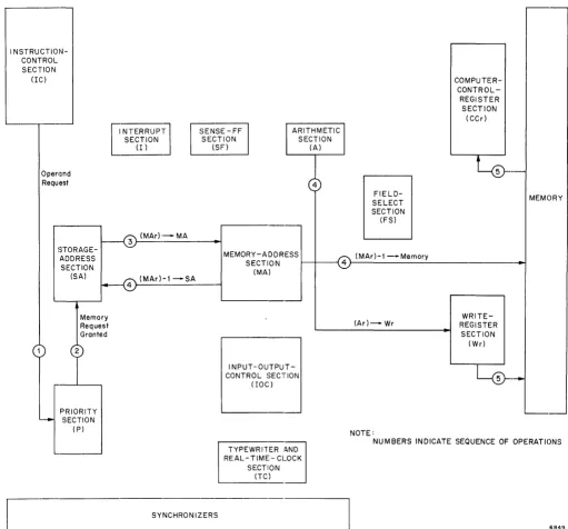
During multiprecision instructions, an operand re·· quest is produced by the instruction-control section (figure 1-3) for each additional operand. When this request is granted, the contents of MAr are trans·· ferred to the memory-address section where they are decreased by 1. This modified address is then transferred to memory and also baok to the MAr. The contents of the memory location, represented by the modified address, are read from memory into CCr during a read operation, or the contents
I NSTRUCTIOI\I-CONTROL SECTION
(IC)
OpercJnd Request
(MAr)-MA
of the write register are written into the mernory location during a write operation.
1-38. Data Flow During Instructions Which Use the Main Adder
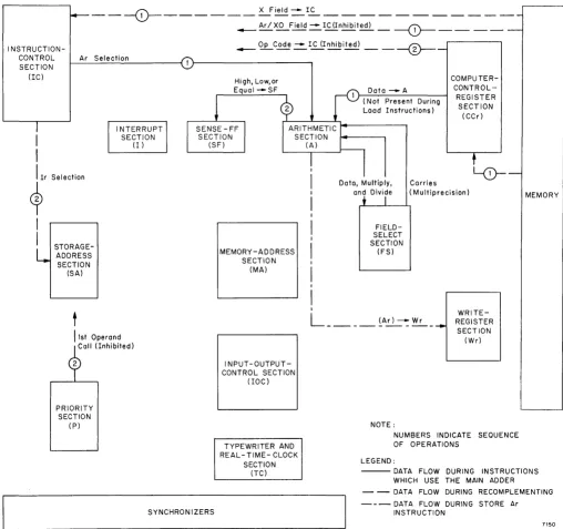
The data flow is similar for all instructions which use the main adder. These instructions include the add, subtract, compare, logical operations, and ex-tract instructions (figure 1-4). The operand in the CCr is transferred to the arithmetic section and is combined with the contents of the specified accumu-lator registers. The specific differences anlOng
FIELD-SELECT SECTION (FS)
COMPUTER-
CONTROL-REGISTER SECTION
(CCr)
MEMORY
STORAGE-ADDRESS SECTION
MEMORY-ADDRESS 1--+---14 (MAr)-I-Memory SECTION
(SA)
Memory Request Granted
PRIORITY SECTION
(P)
~-l-SA (MA)
INPUT-OUTPUT-CONTROL SECTION
(rOC)
TYPEWRITER AND;
REAL-TIME- CLOCK SECTION
(TC)
~
SYNCHRONIZERSL ___ .
_ _ _ _ _
.
=
(Ar)- Wr
NOTE:
WRITE-REGISTER
SECTION
(Wr)
NUMBERS INDICATE SEQUENCE OF OPERATIONS
6849
Introduction and General Description
---0---~~~I.£...---_Ar/X-2-Field~IC(In~t~ -
--0---I NSTRUCT--0---ION- NSTRUCTION-CONTROL SECTION
(IC)
Ar Selection
_<2..LCode~I..£J..Inhibi~ _ _ ~
IIr Selection
~
I
High, Low,or
Equal-SF Data - A
(Not Present During Load Instructions)
Carries
COMPUTER- CONTROL-REGISTER SECTION
(CCr)
Data, Multiply,
and Divide ( Multiprecision) MEMORY
I
STORAGE-ADDRESS SECTION(SA)
MEMORY-ADDRESS SECTION
FIELD-SELECT SECTION (FS)
t
11st Operand Call (Inhibited)
(MA)
WRITE-L _____
~A~___:~ _ _. REGISTER SECTION(Wr)
INPUT-OUTPUT-CONTROL SECTION
(roC)
PRIORITY SECTION
(P) NOTE:
TYPEWRITER AND REAL-TIME- CLOCK
SECTION
NUMBERS INDICATE SEQUENCE OF OPERATIONS
LEGEND: (TC)
SYNCHRONIZERS
- - - DATA FLOW DURING INSTRUCTIONS WHICH USE THE MAIN ADDER
- - DATA FLOW DURING RECOMPLEMENTING - - - DATA FLOW DURING STORE Ar
INSTRUCTION
7150
Figure 1-4. Data Flow During Instructions Which Use the Main Adder, Functional Block Diagram
instructions are produced through different methods of gating the operands into the main adder. During these instructions, the memory request for the next instruction is made while the last operand is being read into the arithmetic section.
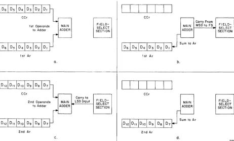
When multiprecision arithmetic operations are spec-ified, the word containing the least significant bits is transferred to the main adder first, and the word containing the most significant bits is transferred last. The carry from the most-significant-bit posi-tion of one word is stored in the field-select sec-tion during a multiprecision operasec-tion. The carry is then supplied to the least-significant-bit position of the next word (figure 1-5).
Central Processor Logic
1 st Ar
Q.
2nd Ar
c.
MAIN ADDER
Corry to MAIN LSD Input
ADDER
FI ELD-SELECT SECTION
FI ELD-SELECT SECTION
CCr
1 st Ar
b.
CCr
2nd Ar
d.
Corry From MAIN MSD to FS ADDER
MAIN ADDER
FI ELD-SELECT SECTION
FIELD-SELECT SECTION
7151
Figure 1-5. Example of Double-Precision
Add
with Carries, Functional Block Diagramoperation-code field and the AR/XO-field then are transferred to the instruction-·control section, and the first operand is read from memory.
1-40. HIGH, LOW, AND EQUAL FLIP-FLOPS. Dur·· ing the add, subtract, and compare instructions, there is an output from the arithmetic section which sets flip-flops in the sense-FF section. The add and subtract instructions set the equal F'F if the result equals zero, and reset it if the result does not equal zero. The compare instructions set the appropriate flip-flop (high, low, or equal).
1-41. EXTRACT INSTRUCTIONS. The contents of the fields to be extracted during an extract instruc-tion are determined by the field-select FF's in the same way that the fields are determined during field selection. Therefore, field selection must be deSignated for an extract instruction; otherwise, the extract instruction will function in the same way as a load-Ar instruction.
1-42. MULTIPLY AND DIVIDE INSTRUCTIONS. The multiply and divide instructions are done by successive additions and subtractions. The 48-bit dividend occupies Ar1 and Ar2 and the divisor is contained in the CCr. The quotient is placed in Ar2 and the remainder is placed in Arl. The multiplier occupies Ar1 and the multiplicand is contained in the CCr; the 48-bit product is plaoed in Ar2 and Ar3. Shifting in both the multiply and divide opera-tions is done by routing the data through the field-select section.
1-43. STORE- AND LOAD-ACCUMULATOR
][N-STRUCTIONS. During the execution of the aCCUD1U-lator store instruction, data are transferred from the specified Ar' s directly to the write register, and from there into memory. During the execution of the multi word load instructions, the contents of adjacent memory locations may be transferred to any designated set of Ar's. During the execution of the multiword store instructions, the contents of any set of Ar's can be transferred to adjacent mem-ory locations. The only restriction is that the con-tents of the lowest numbered Ar occupy the last memory location during a store instruction and that the lowest numbered Ar receives the input from the last memory location during a load instruction.
Figure 1-6 shows the storing of three words from adjacent memory locations into three non-adjacent Ar's, and figure 1-7 shows the storing of the con-tents of two Ar's in adjacent memory locations.
MEMORY LOCATIONS
ACCUMULATOR REGISTERS
"7152
MEMORY LOCATIONS
ACCUMULATOR REGISTERS
Figure 1~7. Storing Contents of Accumulator into Adjacent Memory Locations, Diagram
I NSTRUCTION-CONTROL SECTION
(rc)
7153
Introduction and General Description
1-44. Data Flow During Instructions Which Transfer Data Between the Storage-Address Registers and Memory
The instructions which transfer data between the storage-address registers and memory are these:
Instructions which: store the contents of a SAr (figure 1-8);
Instructions which load a SAr from memory (fig-ure 1-8); and
Instructions which either modify, or modify and compare the contents of an Ir (figure 1-9).
COMPUTER-(CCR 1 - 15) - MA
CONTROL-1 - - - REGISTER
I SECTION
SAr Selection
~
I
I
Priority Request
(MAr) - FS
(SAr)- MA
STORAGE-~~~---;
ADDRESS SECTION
(SA) (CC~~)=~
2
PRIORITY SECTION
(P)
SYNCHRONIZERS
I
I
I
cP
I
(MAr) - MA
FIELD-SELECT SECTION (FS)
(CCr)
MEMORY-ADDRESS
SECTION j---..:.{...;..M_A.:....;rl_----..,;M.;.;,.e;;.;.m;.;.,;o:;,.;..r.L--_ _ _ _ _ _ _ _ _ _ -{ 4 (MA)
I NPUT-OUTPUT-CONTROL SECTION
(roC)
TYPEWRITER AND REAL- TIME- CLOCK
SECTION (TC)
(SAr)-Wr
NOTE:
LEGEND:
WRITE-REGISTER
SECTION (Wr)
NUMBERS INDICATE SEQUENCE OF OPERATIONS
- - - DATA FLOW DURING SAr STORE INSTRUCTION
- - DATA FLOW DURING SAr LOAD INSTRUCTION
MEMORY
7154
Central Processor Logic
I NSTRUCTION-CONTROL SECTION
(IC)
I NTERRUPT
J
SECTION (I)
(CCR 10-24) -MA
1
-I
(CCR 1-9) - MACOMPUTER-
CONTROL-REGISTER SECTION
(CCr)
L--~l
I r Selection High,Low,I
or Equal - SFL
I
I
I
I
I
Ir-Control Word( I r ) -MAS
STORAGE-ADDRESS (Ir)± (CCR 1-9)- Ir SECTION
(SA)
PRIORITY SECTION
(P)
( I r ) - MAS
MEMORY-ADDRESS SECTION
(MA)
INPUT-OUTPUT-CONTROL SECTION
(lOC)
FIELD-SELECT SECTION (FS)
NOTE:
WRITE-REGISTER
SECTION (Wr)
MEMORY
TYPEWRITER AND I
REAL- TIME- CLOCK SECTION
(TC)
LEGEND:
NUMBERS INDICATE SEQUENCE OF OPERATIONS
- - DATA FLOW DURING Ir MODIFY INSTRUCTION
r---
SYNCHRONIZERS~
~----~
- - ADDITIONAL DATA FLOW DURING MODIFY -AND-COMPARE INSTRUCTION
7155
Figure 1-9. Data Flow During Index-Register Modify and Compare Instructions, Functional Block Diagram
1-45. DATA FLOW DURING INSTRUCTIONS WHICH STORE THE CONTENTS OF A STORAGE-ADDRESS REGISTER. When the first operand is read from memory during a store-SAr instruction, another memory request is made. When memory access is granted, the contents of the SAr specified by the AR/ XO-field of the instruction are transferred through the memory adder to the write register. The m' ad-dress is sent from MAr through the field-select section to the MAS. The contents of the MWr, which contain the contents of the SAr, then are transferred to the memory location specified by the MAr.
1-46. DATA FLOW DURING INSTRUCTIONS WHICH LOAD A STORAGE-ADDRESS REGISTER. During
the execution of the load-SAr instructions, the first 15 bits of the operand in the CCr are transferred through the memory-address section to the SAr specified by the instruction-control section. The re-quest for the next instruction is made while data are being transferred to the register.
con-tents of the Ir sp~cified by the AR/XO-field of the instruction. The modified contents of the Ir are then returned to the same Ir.
If the instruction calls for a comparison, the clearing of the CCr is inhibited and the contents of the CA-field of the control word are then subtracted from the modified contents of the Ir. The result of the subtraction sets the appropriate high, low, or equal indicator in the sense-FF section.
1-48. Data Flow During Shift Instructions
During the execution of the shift instruction, the shift count, which is contained in the four least sig-nificant bits of the contents of the MAr, is transferred to the field-select section after the m' address has been placed in the MAr. The contents of the Ar's specified by the AR/XO-field are then transferred to the CCr. The contents of the CCr are shifted according to the type of shift instruction and then returned to the Ar' s. The shifting is terminated by an end-of-shift signal from the field-select section.
The CCr performs only right decimal shifts (four bits at a time) and right binary shifts. Thus, all shifting must be performed by combinations of the two types of right shifts. Alphanumeric shifts are performed by combining decimal shifts and binary shifts. Left shifts are performed by translating the left shift counts into right shift counts.
For example, the 2-digit left shift of the six digits represented by A through F in figure 1-10 could be done by either of two methods. The first method would consist of transferring all the digits from one register to another register and then performing a 2-digit left shift (a and b of figure 1-10). The second method would consist of shifting one digit at a time from the four least-significant-bit pOSi-tions of one register into the four most-significant-bit positions of another register, and repeating this shifting four times (c of figure 1-10). The latter method performs the left shift by using the right-shift operation and is the method used in the UNIV AC
lIT system.
Figure 1-11 shows the data flow for shifting right two digit positions, and figure 1-12 shows the data
0 C B
a.
Introduction and General Description
flow for shifting left two digits during double-precision shift instructions. The data flow for single-precision shift instructions is shown in e, f, and g of figure 1-11 and in e and f of figure 1-12. The letters A through L represent 4- bit decimal digits.
1-49. Data Flow During Miscellaneous Instructions
The miscellaneous instructions are these:
The sense- F F instructions (figure 1-13);
The test-interrupt instructions (figure 1-13);
The expand instruction (figure 1-14);
The compres s instruction (figure 1-14);
The transfer instructions;
The zero-suppress instruction; and
The typewriter instructions (figure 1-13).
1-50. SENSE - FLIP - FLOP INSTRUCTIONS. The sense- FF instructions include all instructions which set, reset or test the flip-flops in the sense-FF section. A specific flip-flop is selected by the de-coded output of the AR/XO-field. If the instruction requires testing the flop output, and if the flip-flop is set, the m' address is placed in the CC rather than in the MAr. This transfer which is controlled from the priority section, causes the program to jump to the instruction in the location specified by the address of the test instruction.
1-51. INTERRUPT INSTRUCTIONS. During the ex-ecution of an instruction which tests or resets the interrupt FF's, the specific flip-flop is addressed through a combination of the AR/XO-field and the m-ADDRESS field. The AR/XO-field specifies a class-l or -2 interrupt, or a priority channel in a class-3 interrupt; the m-ADDRESS field speCifies the specific flip-flop. If the instruction calls for testing the flip-flop, and if the flip-flop is set, the next sequential instruction is performed; if the flip-flop is reset, 2 is added to the contents of the C C when the next instruction is read from memory. Thus, one instruction is skipped if the flip-flop is reset.
F1E~
I
AI
~
0 C B Ar-]
b. c. 7156
Central Processor Logic
~TKIJIII
H G L KIJ=r~0
L KJ
II
HI
G ]1 st Ar 1st Ar 1st Ar
~I
E 10I c I
B AF
EID~
F
EI
0I c I
B A2nd Ar 2ndo.r 2nd Ar
y
eLI
F
EI~cl
B ACCr CCr CCr
O. Initial Conditions b. 2nd Ar - - - CCr C. CCr (2 Shifts); 1st Ar - CCr
~I
KI J
IIHIGI
L K,.QI
L KJ
II H
I
G
J
1 st Ar 1st Ar 1 st Ar
~I
GI
F
EI
0I
c
H G
I
QE
I
0 CH G
I FIE I
0I
c
12nd Ar 2nd Ar 2nd Ar
CI
I
I I
y
L KI
ITI
I
HG
I
LI
KI
J
I
IJ
CCr CCr CCr
d. CCr - 2nd Ar e. 1 st Ar-CCr 1. CCr (2 Shifts)
I
11K
I
J I1st Ar
I
HI
GIUE
I
0 C2nd Ar
l=r
CCr
g. CCr - 1 s t Ar
7157
Figure 1-11. Data Flow During Double··Precision Two-Digit Right Shift, Diagram
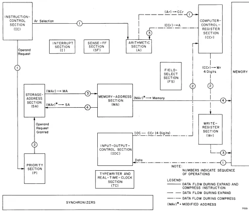
1-52. DATA FLOW DURING THE EXPAND IN-STRUCTION. The expand instruction converts 12
4-bit decimal digits (2 words contained in the Ar's) into 12 6-bit alphanumeric characters which are stored in
a
words in memory. When memory access is granted, the first word to be converted is trans-ferred from the specified Ar to the CCr, and a memory request is made in order to write a word into memory. When memory access is granted, the first four digits of the first word are transferred to the write register where the two zone bits are added. The word then is written into the memory location specified by the address in MAr. For the storing of subsequent words, a new memory requestis made and the process is repeated. The cont1ents of MAr are decreased by 1 after the first word is read from memory.
Three memory request are made during the expand instruction; the first to store the first four dtgits of the first decimal word; the second to store, the last two digits of the first decimal word and the first two digits of the second decimal word; and the third to store the last four digits of the second dectmal word.
- - -
-Introduction and General Description
ILIK
J I H G L K J I H G1 st Ar 1 st Ar 1 st Ar
F
EIDlcis
A2nd Ar 2nd Ar
LjJ
rIHIGIFIE}--CCr CCr CCr
a.Initial Conditions b. 2nd Ar ---- CCr C. CCr (4 Shifts); 1 st Ar --+ CCr
J H G F
I
EJ J I HI
GI FIE]
1 st Ar 1 st Ar 1 st Ar
2nd Ar 2nd Ar
CCr CCr CCr
d. CCr--' 1 s1 Ar e. 2nd Ar---' CCr (4 Shifts) f.
7158
Figure 1-12. Data Flow During Double-Precision Two-Digit Left Shift, Diagram
three alphanumeric words from memory, con-verts these into two decimal data words, and trans-fers the two words to two Ar's. The word to be compressed is transferred from memory to the input-output control section, and only the numeric bits are transferred from the input-output control section to the CCr. The data are then transferred from the CCr to the Ar's specified by the AR/XO-field of the instruction.
Three memory accesses are required for the com-press instruction. During the execution of the first memory access, the first alphanumeric word is read from memory and the four digits are read into the first four digit positions of the first Ar. Dur-ing the execution of the second memory access the second alphanumeric word is read from memory and the four decimal digits are transferred to the fifth- and sixth-digit position of the first Ar and to the first- and second-digit position of the second Ar. During the execution of the third memory access, the third alphanumeric word is read from memory and the four decimal digits are transferred to the last four-digit positions in the second Ar.
1-54. DATA FLOW DURING TRANSFER INSTRUC-TIONS. The transfer instructions cause the program to execute the instruction contained in the m' ad-dress location rather than the next sequential in-struction in the program. This is done by decoding
the first operand as an instruction and storing the m' address in the CC rather than the MAr.
1-55. DATA FLOW DURING ZERO-SUPPRESS IN-STRUCTION. During the execution of the zero-suppress instruction, the output of the CCr is de-coded to produce signals which represent decimal O's or commas. These signals then are transferred to the field-select section which uses the same process to eliminate the zeros as is used in select-ing the fi