to interface electronic structure and stability against chemical
phase separation
C. Krug and G. Lucovskya)
Department of Physics, North Carolina State University, Campus Box 8202, Raleigh, North Carolina 27695
共Received 22 December 2003; accepted 29 March 2004; published 19 July 2004兲
Extensive spectroscopic characterization of high k materials under consideration for replacing Si oxide as the gate dielectric in Si-based microelectronic devices has been accomplished. Band offset energies of Zr silicates with respect to Si have been determined as a function of silicate alloy composition by combining near-edge x-ray absorption fine structure spectroscopy, vacuum-ultraviolet spectroscopic ellipsometry, x-ray photoelectron spectroscopy 共XPS兲, Auger electron spectroscopy, and ab initio calculations on cluster models. These studies provide insight that applies to both transition metal- and rare earth-based dielectrics, including binary oxides and silicate and aluminate alloys. Results have been used to estimate the electronic conduction through Hf silicate films as a function of alloy composition. Thermally induced chemical phase separation in Zr silicate films has been characterized using XPS, Fourier transform infrared spectroscopy, x-ray diffraction, high-resolution transmission electron microscopy, and extended x-ray absorption fine structure spectroscopy. Our results indicate separation into a noncrystalline, Si-rich phase and either nano- or microcrystalline ZrO2, depending on the original film stoichiometry. © 2004 American Vacuum Society. 关DOI: 10.1116/1.1755714兴
I. INTRODUCTION
The search for a material of high dielectric constant共high
k兲 to replace nitrided silicon oxide as the gate dielectric in advanced microelectronic devices has been concentrated on Hf and Zr-based materials. The pure transition metal oxides are naturally attractive due to their high k values, but silicate alloys have shown enhanced thermal stability against crys-tallization. Additional issues that have been addressed re-garding thin high k films on Si include: band alignment, in-terfacial electronic states, fixed charge, charge trapping, electron mobility at the interface with Si, and reliability with respect to dielectric breakdown. The vast knowledge base available regarding the SiO2/Si interface has been of limited
use, and new understandings need to be developed.
In this article we use spectroscopic data to address共i兲the band alignment of transition metal silicates with Si and 共ii兲 chemical phase separation during thermal annealing of Zr silicate alloys. In the first case, we build models that ulti-mately identify the optimal silicate alloy composition regard-ing suppression of direct electron tunnelregard-ing. In the second, we present a wealth of experimental data that support a re-cent analysis of the thermodynamics of the Si–O–Zr system. Our experimental data are the result of extensive spectro-scopic characterization of Hf and Zr silicate alloys using x-ray absorption spectroscopy 共XAS兲, including extended x-ray absorption fine structure共EXAFS兲and near-edge x-ray absorption fine structure 共NEXAFS兲 spectroscopies, vacuum-ultraviolet spectroscopic ellipsometry 共VUV SE兲, x-ray photoelectron spectroscopy 共XPS兲, Auger electron spectroscopy共AES兲, Fourier transform infrared spectroscopy
共FTIR兲, x-ray diffraction 共XRD兲, and high-resolution trans-mission electron microscopy共HRTEM兲.
II. EXPERIMENTAL PROCEDURES
XPS, AES, XAS, VUV SE, and HRTEM measurements were performed on Hf and Zr silicate films ranging in thick-ness from 20 to 50 nm on Si共100兲; films thicker than 150 nm were deposited:共i兲on Si共100兲for FTIR and XRD and共ii兲on fused silica for XAS measurements. The remote plasma en-hanced chemical vapor deposition 共RPECVD兲 process used for sample preparation is described in detail elsewhere.1,2In summary, radio frequency excitation共13.56 MHz, 15 W兲of a He/O2(20:1) mixture produces a plasma. Excited species reach the sample holder in the plasma afterglow region as a result of gas flow. Si and Zr 共Hf兲source gases关2% SiH4 in
He and Zr共IV兲t-butoxide共Hf共IV兲t-butoxide兲carried by He兴 are delivered directly onto the substrate by two different shower-head injectors. The substrate is kept at 300 °C, and the total pressure during deposition is 0.3 Torr.
Changing the flow rates of the transition metal and Si source gases varied the composition of the deposited films. Substrates were treated in a H2O/HF (100:1) solution prior
to film deposition to remove the superficial native oxide. Also,⬃3 nm of a-SiO2 were deposited on the Si substrates
by RPECVD before silicate deposition. This had two pur-poses:共i兲to suppress reactions of the Zr共Hf兲source gas with the Si substrate and 共ii兲 to prevent reactions between the alloy and the Si substrate during postdeposition annealing. Thermal annealing was performed ex situ in an inert Ar am-bient for 1 min.
The composition of silicate alloys, reported as x in (MO2)x(SiO2)1⫺x 共M⫽Zr,Hf兲, was obtained from on-line
a兲Author to whom correspondence should be addressed; electronic mail:
AES measurements using the ratio of the derivative spectrum peak-to-peak heights of ZrM NN( M VV)and OKLL(KVV)features. The Auger process was initiated by a 3 keV electron beam, which was defocused to prevent damage to the samples. These measurements were once calibrated against Rutherford backscattering spectrometry, which indicated that the alloy films are homogeneous and fully oxidized; the uncertainty in composition is ␦x⫽⫾0.03. FTIR absorption measurements, in the mid-IR共4000– 400 cm⫺1兲and far-IR共700–50 cm⫺1兲, were performed in the transmission mode. XPS measure-ments of O 1s, C 1s, Zr 3d, and Si 2 p core levels were made using nonmonochromatized Mg K␣ radiation 共1253.6 eV兲 and a pass energy of 20 eV. Data were corrected for charging effects using the C 1s peak at 284.6 eV from ad-ventitious carbon contamination on the sample surface. EX-AFS and NEXEX-AFS measurements were made at the National Synchrotron Light Source at Brookhaven National Labora-tory. Absorption spectra for the O K1 edge NEXAFS were
recorded by detecting the primary photoelectron yield, and absorption data for EXAFS and NEXAFS at the Zr K1 edge
were obtained by monitoring x-ray fluorescence. Ab initio calculations have been discussed in detail elsewhere.3
III. BAND ALIGNMENT WITH RESPECT TO Si
In the following we show the application of various spec-troscopic techniques to the determination of band alignment at the transition metal silicate/Si interface as a function of
silicate composition.2,4,5 Our results qualitatively apply to transition metal aluminate alloys as well. Starting from the electronic structure of ZrO2, we use spectroscopic data to
analyze the silicate conduction and valence band edges, thus building the complete band diagram. We then consider atomic d-state energy as a scaling variable for the electronic properties of transition metal- and rare earth-based dielec-trics. Finally, we develop a model to estimate electron tun-neling through silicate alloys as a function of silicate
com-position.
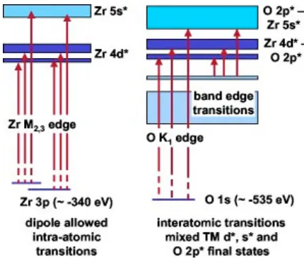
Figure 1 is a schematic representation of the intra- and interatomic electronic transitions for ZrO2that are addressed
in this article. The intra-atomic transitions are dipole allowed and reflect the atomic states of Zr, while the interatomic tran-sitions terminate in mixed Zr and O states, and therefore are qualitatively different than the intra-atomic transitions. The relative ordering of the conduction band states is supported by molecular orbital calculations of small clusters incorpo-rating group IVB Ti, Zr and Hf atoms in octahedral and tetrahedral bonding arrangements with oxygen neighbors.6 – 8 The top of the valence band is associated with nonbonding oxygen 2 p states, and the first two conduction bands are associated with transition metal d states. The energy separa-tion between the top of the valence band in ZrO2 and the
threshold absorption to the O 2 p* states mixed with Zr 5s* states defines an ionic band gap of essentially the same width as in nontransition metal insulating oxides such as MgO or Al2O3, ⬃8 –9 eV.
7,9
The lowest conduction band states of ZrO2as determined
from XAS and VUV SE measurements are associated with
Zr 4d* states. Figure 2共a兲 displays the deconvolved Zr M3
NEXAFS spectrum of crystalline ZrO2, which displays
fea-tures associated with transitions from Zr 3 p3/2 states to
Zr 4d* 共split兲 and Zr 5s* states. The symmetry-determined splitting of the 4d*states in Table I is designated as⌬(d*), and the energy separation between the lowest 4d*state, and the center of the 5s* band is designated as ⌬(d*,s*). The table includes experimental results for ZrO2M2,3 and
HfO2N3spectra. The splitting of the 5d*states in the Hf N3
spectrum is not spectroscopically resolved due to an increase in linewidth that scales with atomic number. Table II in-cludes the spectroscopically determined spin-orbit splittings of Ti, Zr, and Hf p1/2and p3/2states. Figure 2共b兲displays the O K1NEXAFS spectrum of crystalline ZrO2. The two bands at the low photon energy edge are associated with transitions to mixed O 2 p*⫺Zr 4d* states. A third multi-component band has considerable O 2 p*character, mixed with Zr 5s*, and additional features at higher energies due to mixing with Zr 5 p*states. Table I includes the⌬(d*) splitting, as well as the energy separation between the lower energy d*state and the first spectral peak of the 5s* band, ⌬(d*,s*). Figure 2共c兲displays the band edge optical absorption constant␣of ZrO2 obtained from analysis of VUV SE data. The lowest
lying transitions in the crystalline ZrO2O K1 edge and band
gap transitions are associated with Zr 4d* states.
The assignments in Fig. 2 are based in part on compari-sons with the results of our ab initio calculations. The ab
initio method used is based on a self-consistent field
Hartree–Fock calculation, followed by a configuration inter-action共CI兲refinement utilizing the variational theorem. Pro-ceeding in this way, the calculations include final state ef-fects, in particular the Coulomb attractions between core and valence band holes, and the excited electrons. Table I sum-marizes the energy splittings, ⌬(d*) and ⌬(d*,s*), of the band edge electronic states for ZrO2 and HfO2as determined
FIG. 1.共Color online兲Schematic representation of the intra-atomic Zr M2,3,
and interatomic O K1and band edge transitions for ZrO2. The ordering of
from experiment. The agreement between calculations and experiment is in the range of⫾0.3 eV.
Figure 3共a兲compares O K1NEXAFS data for a Zr silicate
alloy (x⬃0.6) after a 900 °C anneal in共i兲, and as deposited in共ii兲. The spectrum in共i兲is well approximated by a linear combination of the crystalline ZrO2O K1 spectrum of Fig. 2共b兲, and the SiO2O K1 spectrum. In the noncrystalline
as-deposited film共ii兲, the higher energy component of the Zr d* doublet overlaps the Si 3s*band and is not spectroscopically resolved. The Si 3s* and Zr 5s* states overlap with no re-solvable features that can be assigned to either atomic state. The Zr 4d* state remains the lowest-lying conduction band state, and hence defines the onset of band gap transitions as
in ZrO2. Studies of Zr silicate alloys with 0.35⬍x⬍0.70
establish that the separation between the Zr 4d* and Si 3s* features is constant, but their relative intensities scale with alloy composition. A similar behavior occurs for Hf silicate alloys. This is shown in Fig. 3共b兲for noncrystalline Hf sili-cate alloys, where the Hf 5d*state replaces the Zr 4d*state as the lowest energy transition. Our most important observa-tion is that the conducobserva-tion band edge, and therefore the con-duction band offset energy with respect to Si in Zr and Hf silicate alloys is associated with the respective transition metal d* states and does not change in energy with silicate
bonding. It is effectively pinned at the transition metal oxide
value. A similar conclusion applies to Zr and Hf aluminate alloys, where the decrease in the band gaps between noncrys-talline Al2O3and SiO2, results in increased overlap between the Al 3s* state and respective transition metal d* states.
Having analyzed the transition metal silicate 共and alumi-nate兲 conduction band edge, we now address the valence
FIG. 2. ZrO2spectra:共a兲Zr M3 and共b兲O K1 edges from XAS
measure-ments, and共c兲optical absorption constant from VUV SE.
TABLEI. Experimentally determined⌬(d*) and⌬(d*,s*) energy splittings
for ZrO2and HfO2.
Spectrum
Energy共⫾0.2 eV兲 Energy共⫾0.3 eV兲
d1* d2* s* ⌬(d*) ⌬(d*,s*)
ZrO2– Zr M2 345.9 347.7 357.5 2.2 11.7
ZrO2– Zr M3 332.6 334.8 344.5 2.2 11.9
ZrO2– O K1 532.2 535.4 542.3 3.2 10.1
HfO2– Hf N3a 382.7a 382.7a 392.7 ⬍3.5b 10a
HfO2– O K1 532.5 536.8 541.5 4.3 9.0
aDoublet is not spectroscopically resolved. bEstimated from linewidth.
TABLEII. Spin-orbit splittings of p-state.
Oxide
p-state spin-orbit splitting共⫾0.5 eV兲
TiO22 p ZrO23 p HfO24 p
XAS spectra 5.6 13.3 57.0
Data Handbooka 6.4 13.7 57.5
a
band edge. For the AES OKLL process in SiO2 it has been
demonstrated that L refers to nonbonding O 2 p states at the top of the valence band.10Thus
EK共OKLL兲⫽EB共O 1s兲⫺2EB共O 2 p兲⫺⍀,
EB共O 2 p兲⫽1/2关EB共O 1s兲⫺EK共OKLL兲⫺⍀兴, 共1兲
where EK is the electron kinetic energy from AES, EB is an electron binding energy from XPS, and ⍀includes all final state and Coulomb effects. Under the hypothesis that the same applies to the high k materials under consideration, Eq. 共1兲can be used to estimate EB(O 2 p) within⍀using OKLL AES and O 1s XPS data. This sets the stage for establishing
EB(O 2 p), the valence band edge energy, as a function of high k alloy composition.
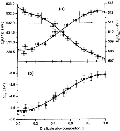
Figure 4共a兲displays OKLLAES and O 1s XPS data for Zr silicates in the whole range of possible compositions (0⬍x
⬍1). XPS and UPS measurements have established that the valence band offset energies with respect to Si⌬EV are 4.6
eV for SiO2(x⫽0) and 3.1 eV for ZrO2(x⫽1).11,12Starting from these values we apply a scaling with silicate
composi-tion that follows Eq. 共1兲to arrive at
⌬EV共x兲⬇⫺A•1/2•关EB共O 1s兲⫺EK共OKLL兲兴⫹B, 共2兲
with A⫽0.44 and B⫽1.2. Figure 4共b兲displays the data cor-responding to Eq.共2兲. The nonlinear change in valence band edge with silicate composition corresponds to changes in the average O-atom bonding coordination, which increases from 2 in SiO2 to 3 in (ZrO2)0.5(SiO2)0.5, and to 4 in ZrO2.
Figure 5 is the result of merging our findings regarding FIG. 3. Comparison of XAS O K1edges for共a兲Zr and共b兲Hf silicates.共a兲
Compares crystalline and phase-separated Zr silicate with x⬃0.6, and共b兲 compares Hf silicate alloys with the SiO2 concentration increasing from ⬃0.25 to 0.75共bottom to top兲.
FIG. 4. 共a兲 XPS O 1s binding energy and AES OKLLkinetic energy as a function of Zr silicate alloy composition.共b兲Valence band offset with re-spect to Si⌬EVas given by Eq.共2兲.
FIG. 5. Compositional dependence of band offset energies for Zr silicate
high k conduction and valence band edges and alignment to Si. With x increasing from 0 (SiO2) to 1 (ZrO2), one
ob-serves that:
• the conduction band offset is reduced. It is the same for the silicates and ZrO2and does not change with silicate
com-position;
• the valence band offset is reduced. It is higher for the silicates as compared to ZrO2;
• the band gap of the dielectric decreases. The silicates show a wider band gap than ZrO2 due to the changing
va-lence band edge.
We have obtained similar results for Hf silicate alloys using VUV SE, XAS, and XPS. XPS data from Hf alumi-nates show the same trend.13Suitable weighting of our spec-troscopic data reproduces the experimental14 optical band gap of Zr and Hf silicates.
Before addressing direct tunneling in silicate alloy sys-tems, we consider transition metal and rare earth atomic
d-state energy as a general scaling variable for high k band
gap and conduction band offset energy. Figure 6 displays the results of an empirical model originally deduced from a com-bination of experiment and model predictions.9 The model demonstrates a monotonic correlation of 共i兲 oxide optical band gaps and 共ii兲 oxide conduction band offset energies with respect to Si to transition metal and rare earth atomic
d-state energy in the s2d␥⫺2 configuration 共␥⫽3 for Sc, Y, and La, 4 for Ti, Zr, and Hf, and 5 for V, Nb, and Ta兲. Based on the previously shown results and discussion, this model qualitatively applies to silicate and aluminate alloys as well. The linear behavior between Ti and Hf and the extension to small d-state energies by Y and La defines the oxides that have received the most interest as potential candidates for replacing SiO2 and Si oxynitrides in complementary
metal-oxide-semiconductor 共CMOS兲 applications. V, Ti, Nb, Ta, and Sc-based materials have been eliminated due to low con-duction band offset with respect to Si—less than ⬃1 eV, taken as a threshold for technological applications due to the
need to suppress electron tunneling. Due to the relevance of this issue we have also investigated electron tunneling through high k silicates as a function of alloy composition.
Equation 共3兲 indicates the tunneling transmission T through a rectangular potential barrier, taken as an approxi-mation for the case of a metal-dielectric-Si capacitor at low bias voltage
T⬀expb⫺2at共Ebm*兲0.5c, 共3兲
where a is a constant, t is the barrier width 共dielectric layer thickness兲, Eb is the barrier height 共conduction band offset兲 and m* is the tunneling electron mass. Taking SiO2 as a
benchmark, t can be rewritten as toxk/kox, where tox is the
equivalent SiO2thickness,15k is the dielectric constant of the
high-k under consideration, and kox is the dielectric constant of SiO2. Based on this picture we define a tunneling figure of merit given by
⌽⫽k共Ebm*兲0.5. 共4兲
Significant increases in k to values of 15–25 in transition metal and rare earth oxides are generally accompanied by decreases in Eb and m*. Using an experimental approach,
16
our group has determined the product Ebm* for HfO2 as
0.23⫾0.01 eV m0 共where m0 is the free electron mass兲.
Based on the spectroscopic studies of Zr oxide and alloys,
Eb⫽1.5 eV has been inferred for Hf oxide and alloys. This corresponds to m*⫽0.15⫾0.02 m0, in good agreement with
other analysis of tunneling through HfO2 films. 17
This mass FIG. 6. Scaling of band gap and conduction band offset with respect to Si
with transition metal and rare earth atomic d-state energy.
is significantly smaller than m*⬃0.55 m0 for electrons in
SiO2 and is consistent with the Franz two band model of Ref. 18.
In order to evaluate how⌽changes with composition for high k alloys, one needs to know the dependence on compo-sition of k, Eb, and m*. We use averages of the values corresponding to the end-member oxides weighted by x; m* in the high k oxide is either estimated from the Franz two band model or experimentally determined. This procedure yields ⌽(x) as displayed in Fig. 7共a兲. The monotonically increasing function for Y silicates predicts that tunneling with respect to SiO2 will be reduced over the entire alloy
range, while the qualitatively different behavior predicts that the tunneling reduction in Hf silicate alloys will display a minimum at an intermediary composition. A Wentzel– Kramers–Brillouin solution of the tunneling problem for 1.2 nm equivalent SiO2 thickness and a potential drop of 1 V
across the dielectric yields the results displayed in Fig. 7共b兲. Experimental data are scaled to an equivalent SiO2thickness
of 1.2 nm assuming tenfold increase in tunneling current per 0.2 nm decrease in equivalent SiO2 thickness.
19
The excel-lent agreement between simulated and experimental data supports our models. Based on our results, x⬃0.6 provides the strongest suppression of electron tunneling in Hf sili-cates. In terms of Si technology, this also means that such silicate—not HfO2—is the most scalable Hf-based
replace-ment for SiO2. Although Hf oxide indeed has a higher k, that effect is mitigated by a decrease in m*.
IV. CHEMICAL PHASE SEPARATION
We now restrict ourselves to Zr silicates and compare spectroscopic data obtained as deposited and after annealing.
We show that there is thermally induced chemical phase separation above 800 °C, and that the mode of separation depends on the metal content of the silicate.20
Figure 8 displays O 1s XPS data. The systematic changes in line shape with alloy composition have been interpreted in terms of changes in the oxygen atom coordination,2as noted above regarding the valence band edge. The spectra in Fig. 8共a兲show asymmetric line shapes, whereas those in Fig. 8共b兲 clearly indicate two discrete and separated spectral compo-nents. The two features in these spectra are assigned to SiO2
-and ZrO2-rich phases. This experimental result supports a
recent analysis of the mixing thermodynamics of the ZrO2– SiO2 system in which the phase separation has been
predicted as a result of spinodal decomposition.21
FTIR data are shown in Fig. 9. As a point of reference, the spectral range includes the Si–O–Si asymmetric stretching signal between 900 and 1300 cm⫺1, the Si–O–Si symmetric stretching 共or bending兲 signal at about 810 cm⫺1, and the Si–O–Si out-of-plane rocking signal at about 450 cm⫺1, all for noncrystalline SiO2.22,23The spectral changes from Figs.
8共a兲to 8共c兲in the as-deposited sample are brought about by alloying with ZrO2. The shoulder at 970 cm⫺1is not present
in noncrystalline SiO2; it has been assigned 24
to a stretching vibration of a terminal Si–O bond formed by disruption of the SiO2 network upon formation of a pseudobinary alloy
with ZrO2. 25,26
The spectrum for x⫽0.50 in Fig. 9共b兲is for a FIG. 8. XPS O 1s spectra for Zr silicate films of various compositions:共a兲as
deposited and共b兲after annealing at 900 °C.
chemically ordered alloy in which the SiO2network has been
completely disrupted. It is comprised of (SiO4)4⫺ ions and
Zr4⫹ ions, where the oxygen atoms have a threefold coordination.2For the samples as-deposited and annealed be-low 900 °C, the first broad feature centered at about 900 cm⫺1is the signature of the (SiO4)4⫺ion. The second broad
feature, centered at approximately 410 cm⫺1, is due to Zr–O vibrations. This assignment is supported by the IR absorption spectrum of a crystalline ZrO2 sample共not shown兲. Spectra in Fig. 9 show essentially no change for annealing at up to 800 °C, consistently with no detectable OH or H2O bands in
the infrared spectrum 共at high wave numbers, not shown兲. The changes observed after annealing at 900 °C are consis-tent with the chemical phase separation inferred from analy-sis of the O 1s XPS data. In particular, a significant decrease of the feature at 970 cm⫺1is consistent with a restriction of terminal Si–O bonding to the boundaries of the SiO2- and
ZrO2-rich phases.
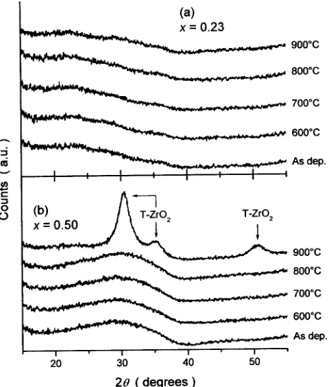
XPS and FTIR results are complemented by XRD data. The broad feature shown for an as-deposited sample with x ⫽0.50 in Fig. 10共b兲does not change after annealing at up to 800 °C, but data obtained after annealing at 900 °C clearly identify the tetragonal crystalline phase of ZrO2. In contrast,
no indication of crystallinity appears in Fig. 10共a兲, which corresponds to a sample with x⫽0.23. This suggests that the details of phase separation depend on the original composi-tion of the silicate. It is interesting to note that the thermo-dynamically favored phase of crystalline ZrO2 at room
tem-perature and pressure is monoclinic. At room temtem-perature,
the tetragonal phase becomes favored at high pressures, which in our sample would be a result of the surrounding SiO2-rich phase.
Figure 11 displays HRTEM images obtained after anneal-ing at 900 °C. The darker regions are assigned to the ZrO2-rich phase. Figure 11共a兲evidences ZrO2 crystallites in a sample with x⬃0.25. Based on the spacing of lattice planes in the Si substrate, the crystallite size ranges from 3 to 5 nm. As mentioned above, these nanocrystallites were not
de-tected by XRD. For example, XRD can readily detect
crys-tallites as small as 10 nm; however, as the crystallite size decreases, the width of an XRD peak increases, and it is generally difficult to detect features as small as 3–5 nm. Figure 11共b兲, which corresponds to a sample with x⬃0.50, shows a microcrystallite that is about 2–3 times larger than the ones in Fig. 11共a兲. Thus, HRTEM identifies the original silicate composition as determining the size of the ZrO2
crys-tallites resulting from phase separation.
Figure 12 displays radial distribution functions 共RDFs兲 obtained from the analysis27 of Zr M2,3 EXAFS data.
As-deposited samples with x⬃0.25 and 0.55 yield essentially the same result, except for a narrowing of the Zr–O peak and reduction of a satellite feature at about 3 Å for low x. An-nealing at 900 °C results in a distinguished feature slightly above 3 Å and in weaker signals below 5 and 7 Å. The peak labeled Zr–Zr corresponds to a second-nearest neighbor dis-FIG. 10. XRD data for Zr silicate films of different composition关共a兲,共b兲兴, as
deposited and after annealing at the temperatures indicated.
tance, and the additional features, to more distant Zr–O and Zr–Zr coordination shells. The three signals resulting from annealing are stronger in the sample with x⬃0.55. The emer-gence of second-nearest neighbor Zr–Zr features is clear evi-dence of order on a crystalline scale. The differences be-tween the RDFs after annealing are consistent with increased crystalline order共crystallite size兲in the alloy with x⬃0.55 as compared to that with x⬃0.25, in agreement with HRTEM data.
V. CONCLUSIONS
We have presented a comprehensive spectroscopic char-acterization of Zr and Hf silicate alloys. Band alignment with respect to silicon has been shown as a function of alloy com-position. The atomic d-state energy of transition metal and rare earth elements has been shown to be a valuable scaling variable for the electronic properties of high k materials. Electron tunneling has been predicted as a function of high k alloy composition in remarkable agreement with
experimen-tal data, showing that (HfO2)x(SiO2)1⫺xwith x⬃0.6 is the most scalable Hf-based high k substitute to Si oxide 共 oxyni-trides兲. Chemical phase separation was observed in the Zr silicate system after annealing at 900 °C and is a point of concern regarding technological applications.
ACKNOWLEDGMENTS
Supported in part by the ONR, AFSOR, SRC, and the SRC/International SEMATECH Front End Processes Center.
1G. Lucovsky, IBM J. Res. Dev. 43, 301共1999兲.
2G. B. Rayner, Jr., D. Kang, Y. Zhang, and G. Lucovsky, J. Vac. Sci.
Technol. B 20, 1748共2002兲.
3
J. L. Whitten, Y. Zhang, M. Menon, and G. Lucovsky, J. Vac. Sci. Tech-nol. B 20, 1710共2002兲.
4G. Lucovsky, J. L. Whitten, and Y. Zhang, Microelectron. Eng. 59, 329 共2001兲.
5G. Lucovsky, Microelectron. Reliab. 43, 1417共2003兲. 6
C. J. Ballhausen and H. B. Gray, Molecular Orbital Theory共Benjamin, New York, 1964兲, Chap. 8.
7P. A. Cox, Transition Metal Oxides 共Oxford Science, Oxford, 1992兲,
Chap. 2.
8G. Lucovsky, G. B. Rayner, Jr., D. Kang, G. Appel, R. S. Johnson, Y.
Zhang, D. E. Sayers, H. Ade, and J. L. Whitten, Appl. Phys. Lett. 79, 1775共2001兲.
9J. Robertson, J. Vac. Sci. Technol. B 18, 1785共2000兲.
10D. E. Ramaker, J. S. Murday, and N. H. Turner, in The Physics of SiO 2 and its Interfaces, edited by S. T. Pantelides 共Pergamon, New York, 1978兲, p. 99.
11
S. Miyazaki and M. Hirose, AIP Conf. Proc. 550, 89共2000兲.
12
S. Miyazaki, M. Narasaki, M. Ogasawaga, and M. Hirose, Microelectron. Eng. 59, 373共2001兲.
13H. Y. Yu, M. F. Li, B. J. Cho, C. C. Yeo, M. S. Joo, D.-L. Kwong, J. S.
Pan, C. H. Ang, J. Z. Zheng, and S. Ramanathan, Appl. Phys. Lett. 81, 376共2002兲.
14H. Kato, T. Nango, T. Miyagawa, T. Katagiri, K. S. Seol, and Y. Ohki, J.
Appl. Phys. 92, 1106共2002兲.
15The equivalent oxide thickness t
ox is the thickness of SiO2 that, in an
MOS capacitor, produces the same capacitance as a thickness t of high k material.
16
C. L. Hinkle, C. Fulton, R. J. Nemanich, and G. Lucovsky, Microelectron. Eng. 72, 257共2004兲.
17T. P. Ma共unpublished兲.
18J. Maserjian, J. Vac. Sci. Technol. 11, 996共1974兲.
19M. L. Green, E. P. Gusev, R. Degraeve, and E. L. Garfunkel, J. Appl.
Phys. 90, 2057共2001兲.
20G. B. Rayner, Jr., D. Kang, and G. Lucovsky, J. Vac. Sci. Technol. B 21,
1783共2003兲.
21H. Kim and P. C. McIntyre, J. Appl. Phys. 92, 5094共2002兲. 22F. L. Galeener and G. Lucovsky, Phys. Rev. Lett. 37, 1474共1976兲. 23
G. Lucovsky, C. K. Wong, and W. B. Pollard, J. Non-Cryst. Solids 59, 60, 839共1983兲.
24G. B. Rayner, Jr., R. Therrien, and G. Lucovsky, Mater. Res. Soc. Symp.
Proc. 611, c13.1共2001兲.
25
J. P. Maria, D. Wicaksana, A. I. Kingon, B. Busch, H. Schulte, E. Gar-funkel, and T. Gustafsson, J. Appl. Phys. 90, 3476共2001兲.
26G. D. Wilk, R. W. Wallace, and J. M. Anthony, J. Appl. Phys. 89, 5243 共2001兲.
27X-Ray Absorption: Principles, Applications, Techniques of EXAFS,
SEX-AFS and XANES, edited by D. C. Koningsberger and R. Prins共Wiley, New York, 1988兲.
FIG. 12. Radial distribution functions from Zr M2,3 EXAFS data for Zr