1157
Simulator Based Design Approach Of
A Feedforward Regulated Cascode Ota
For Sensor Application
Rishi Todani, Tusha Tanya, Ashis Kumar Mal
Abstract: Cascode opamps find wide application in various signal processing circuits. Regulated cascode structures are becoming popular due to faster output stabilization and self bias configuration. However, sizing a cascode structure is a challenge, even for experienced analog designers, due to stacking of several transistors. Devices tend to come out of saturation due to reduced drain source voltage drops. Potential distribution method (PDM), proposed earlier, eliminates this trouble and allows the designer to easily bias the devices in saturation region. It uses the capacity of the simulator to handle complex MOSFET models instead of relying on inaccurate long channel based hand calculations. This paper presents a design technique of a feed-forward regulated cascode OTA using PDM. The steps involved in sizing the devices are clearly discussed and the pre and post layout simulation results are presented. Advanced analysis like PVT and Monte Carlo analysis over input noise is also preformed. Low noise characteristics of the OTA justify its application in low frequency sensor applications. The circuit is designed using SCL 180 nm CMOS technology at 1.8 V supply.
Index Terms:Potential distribution method, PDM, regulated cascode, OTA, input noise, telescopic, simulator based.
————————————————————
1
I
NTRODUCTIONCascode OTAs like telescopic structures are commonly used in analog and mixed signal processing blocks due to their high output impedance. Such structures however suffer from swing issues at input and output due to transistor stacking. Cascode structures could, however, be preferred in sensor applications where swing requirements are not stringent but good noise characteristic is desirable. Biasing cascode structures have always been a challenging task due to stacking of 5 or more transistors. Designers face serious challenge in keeping all transistors in saturation region. Potential distribution method (PDM), given by [5], has provided an innovative technique to eliminate such problems and fine tune performance parameters. This is due to simulator based design approach instead of inaccurate analytical hand calculations. Maintaining saturation region could become even more difficult if complex cross coupling like in regulated structures as given in [1] and [2] are included. In this paper, procedure for designing a fully differential regulated cascode OTA using PDM is illustrated. The steps of device sizing as per PDM are clearly discussed with an example.
2
R
EGULATEDC
ASCODES
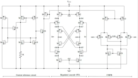
TRUCTUREA regulated cascode OTA structure is shown in Fig. 8 along with the current reference circuit and the common mode feedback (CMFB) circuit. Two pairs of PMOS based regulated cascode, M3/M5 and M4/M6, and two pairs of NMOS based regulated cascodes, M7/M9 and M8/M10 are present. Working together they provide quick current stabilization when a large swing input signal is given. When a large input swing is applied, the differential signal causes the current in the two branches to mismatch. When in+ is at a higher potential then in-, current in left branch becomes larger than right branch.
This causes vb6 to increase and vb7 to decrease. This increases the overdrive of M6 and a decreases the overdrive of M7, nullifying the deviation in current. Similar argument can be put forward for other set of regulation cascodes. The CMFB circuit ensures stable output common mode level.
3 D
ESIGNP
ROCEDUREU
SINGPDM
We design the cascode structure using potential distribution method. It provides a simple mechanism to bias all transistors in saturation region. We start the design by deciding the branch currents. The maximum current is obtained from
maximum power dissipation constraint as
𝐼 =
M i P e di i i
ge (1) Setting Pdiss,max = 80
µW for cascode OTA section and
VDD = 1.8 V, Imax = 44.4 µW is obtained. Minimum current is
obtained from slew rate requirement.
𝐼 = e R e R × L d C ci ce 𝐶 (2) Assuming SR=1.5 V/µs and CL=10 pF, Imin=15 µA is evaluated. We set current of 20 µA in each branch of the cascode structure. All transistor lengths are initially set at 500 nm for suitable analog design. Input and output common mode levels are set to VDD/2 = 0.9 V. Uniform node voltage distribution as [5] is done using the underlying equations. Across each of the six stacked transistors, equal drain source voltages are allotted. 𝑣𝑏3 =
=0.3 (3)𝑣𝑏5 6 = 2 =0.6 (4) 𝑖𝑛 = 𝑜𝑢𝑡 = =
0.9 (5) 𝑣𝑏7 8 = =1.2 (6)𝑣𝑏4 = =1.5 (7) Gate bias of transistors M1, M2, M11 and M12 are set to maintain overdrive around 5% of VDD.𝑣𝑏2 = 𝑉 − |𝑉 +
5% 𝑜𝑓 𝑉 | =1.2 (8) 𝑣𝑏1 = |𝑉 + 5% 𝑜𝑓 𝑉 | =0.6 (9) Bias voltages vb5 through vb8 are such that they are suitable for giving gate bias to corresponding transistors. Using these node potentials, plot of drain current Vs. width is plotted as illustrated in [5] and gate width is read from the graph. Adjacent transistors on the two branches are matched. CMFB and current reference sections are also biased in a similar way and the device dimensions are obtained. Dimensions obtained using PDM is given in Table 1.
_________________________
Rishi Todani obtained is currently working as a Project Faculty in SMDP C2SD program in ECE Department at NIT Durgapur.
E-mail: [email protected]
Tusha Tanya is currently working as Research associate at IIT Delhi and finished her M. Tech. from NIT Durgapur in 2019.
Table 1: Node Voltages
Node Voltage Node Voltage
vb1 0.6 V vb5 0.6 V
vb2 1.2 V vb6 0.6 V
vb3 0.3 V vb7 1.2 V
vb4 1.5 V vb8 1.2 V
in 0.9 V out 0.9 V
4
S
IMULATIONDevice dimensions given in Table 2 were used to create the schematic. After pre layout simulation, layout of the circuit was drawn and post layout simulation was also carried out apart from other advanced analysis. Detailed simulation results are given in Table 6.
Table 2: Device Dimensions
Transistor W/L (µm) Transistor W / L (µm)
M1 11.6/0.5 M16 1/1
M2 11.6/0.5 M17 1/1
M3 33/0.5 M18 8/1
M4 33/0.5 M19 2/1
M5 16.6/0.5 M20 2/1
M6 16.6/0.5 M21 11.6/0.5
M7 3.47/0.5 M22 11.6/0.5
M8 3.47/0.5 M23 11.6/0.5
M9 6.295/0.5 M24 15.3/0.5
M10 6.295/0.5 M25 15.3/0.5
M11 3.095/0.5 M26 15.3/0.5
M12 3.095/0.5 M27 15.3/0.5
M13 1/1 M28 2.99/0.5
M14 4/1 M29 2.99/0.5
M15 2/1
4.1 Stability Analysis
Bode plot of the designed OTA is shown in Fig. 1. Circuit has a high DC gain of around 89 dB with roll-off starting at around 300 Hz. At around 9 MHz the gain plot crosses 0 dB where phase margin is around 88º.
Figure 1: Bode plot
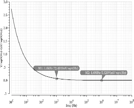
Figure 2: Input noise
4.2 Noise PVT Analysis
The input noise of the OTA is shown in Fig. 2. NMOS input pair, M9 and M10, are the highest contributors to noise (around 43% each). While PMOS input pair, M5 and M6, contribute around 6% each. Noise summary is given in Table 6. N i e f be 15 /√Hz d 40 KHz. L frquency signals, like biomedical or seismic, can be sampled at 40 KHz or higher and fed to this OTA for large amplification. At 1 MHz only thermal noise remains. Noise performance is compared with published literature and is illustrated in Table 6. PVT analysis of the circuit was performed and the corresponding results are tabulated in Tables 3, 4 and 5. Supply voltage corner with 10% variation in VDD was considered. Temperature corners of -50ºC and 100ºC were performed showing satisfactory results.
Table 3: Process corner analysis
Input Noise tt ff ss sf fs @ 1 kHz (nV/√Hz) 72.49 64.46 73.21 66.10 82.88 @ 1 MHz /√Hz 5.32 5.07 5.36 5.21 5.61
Table 4: Supply voltage corner analysis
Input Noise VDD = 1.62 V VDD = 1.98 V @ 1 kHz (nV/√Hz) 64.47 90.39
@ 1 MHz /√Hz 5.60 5.63
Table 5: Temperature corner analysis
Input Noise Temp = −50
◦
C
Temp = 100
◦
C @ 1 kHz (nV/√Hz) 65.62 79.91
@ 1 MHz /√Hz 5.52 5.76
4.3 Monte Carlo Analysis
1159
Figure 3: Monte Carlo – Noise at 1 KHz
Figure 4: Monte Carlo – Noise at 40 KHz
Figure 5: Monte Carlo – Noise at 1 MHz
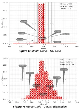
Figure 6: Monte Carlo – DC Gain
Figure 7: Monte Carlo – Power dissipation
4
C
ONCLUSIONPDM proved to be an efficient and quick design tool for sizing complex cascode stuctures like regulated OTAs. It ensured saturation region of operation of all transistors. Estimation of node voltages and currents, a necessary step towards PDM, was clearly discussed and presented. Detailed simulation of the designed OTA, both pre and post layout was carried out. PVT and Monte Carlo analysis over input noise was also c ied d e e ed. I i e f d 72 /√Hz 1 KHz certifies the OTA for sensor applications where good noise characteristic is desirable. The design was carried out using SCL 180 nm CMOS technology at 1.8 V supply.
5
A
CKNOWLEDGEMENTR
EFERENCES[1] You Zheng and Carlos E. Saavedra, “Feedf d-Regulated Cascode OTA for Gig he z A ic i ,” IEEE T c i Circuits and Systems I: Regular Papers, Vol.: 55, Issue: 11, pp. 3373 - 3382, Dec. 2008. [2] Eduard Sackinger, and Walter Guggenbuhl, “A
Versatile Building Block: The CMOS Differential Difference A ifie ,” IEEE Journal of solid-state circuits, vol.sc-22, No.2, April 1987.
[3] P. Mandal and V. Visvanath , “CMO O .A Sizing using a Geometric Programming F i ,” i IEEE T c i C e -Aided Design of Integrated Circuits and Systems, vol. 20, no. 1, pp 22 - 38, 2001.
[4] M. d. Hershenson, S. P. Boyd and T. H. Lee, “O i de ig f CMO -amp via geometric g i g,” i IEEE T c i on Computer-Aided Design of Integrated Circuits and Systems, vol. 20, no. 1, pp. 1-21, Jan 2001 [5] Rishi Todani d A hi K M , “ i
Based
[6] Device Sizing Technique for Operational A ifie ,” W EA T c i
[7] Circuits and Systems, Volume 13, Art. 2, pp.11-28, 2014
[8] Meysam Akbari, Sadegh Biabanifard and Shahroz A di, “I Refe ed Noise Reduction Technique for Yransconductance A ifie ,” E ec ic & Computer Engineering: An International Journal (ECIJ), Vol. 4, No.4, December 2015.
[9] Kai-Wen Yao, Wei-Chih Lin, Cihun-Siyong Alex Gong, Yu-Ying Lin and Muh-Ti hi e, ”A differential difference amplifier for neural recording system with tunable low-f eq e c c ff,” 2008 IEEE International Conference on Electron Devices and Solid-State Circuits, Hong Kong, 2008, pp. 1-4.
[10] . J d A. K. M , ” e ig f i e ifie f e ic i ,” 2017 evice for Integrated Circuit (DevIC), Kalyani, pp. 451-455, 2017.
1161
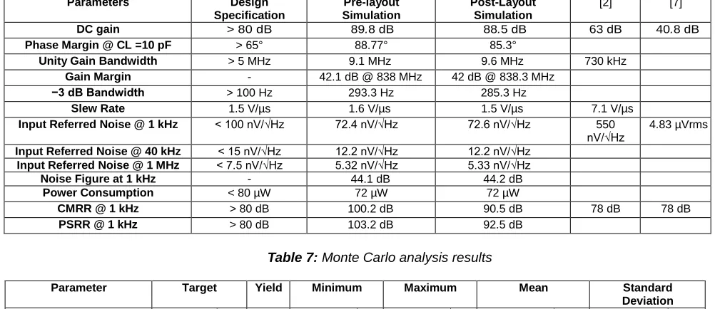
Table 6: Simulation results
Parameters Design
Specification
Pre-layout Simulation
Post-Layout Simulation
[2] [7]
DC gain > 80 dB 89.8 dB 88.5 dB 63 dB 40.8 dB
Phase Margin @ CL =10 pF > 65° 88.77° 85.3°
Unity Gain Bandwidth > 5 MHz 9.1 MHz 9.6 MHz 730 kHz
Gain Margin - 42.1 dB @ 838 MHz 42 dB @ 838.3 MHz
−3 dB Bandwidth > 100 Hz 293.3 Hz 285.3 Hz
Slew Rate 1.5 V/µs 1.6 V/µs 1.5 V/µs 7.1 V/µs
Input Referred Noise @ 1 kHz < 100 /√Hz 72.4 /√Hz 72.6 /√Hz 550 /√Hz
4.83 µVrms
Input Referred Noise @ 40 kHz < 15 /√Hz 12.2 /√Hz 12.2 /√Hz Input Referred Noise @ 1 MHz < 7.5 /√Hz 5.32 /√Hz 5.33 /√Hz
Noise Figure at 1 kHz - 44.1 dB 44.2 dB
Power Consumption < 80 µW 72 µW 72 µW
CMRR @ 1 kHz > 80 dB 100.2 dB 90.5 dB 78 dB 78 dB
PSRR @ 1 kHz > 80 dB 103.2 dB 92.5 dB
Table 7: Monte Carlo analysis results
Parameter Target Yield Minimum Maximum Mean Standard
Deviation Input Noise @ 1 kHz < 80 /√Hz 100 72.36 /√Hz 72.63 /√Hz 72.49 µ /√Hz 42.42 /√Hz Input Noise @ 40 kHz < 15 /√Hz 100 12.26 /√Hz 12.27 /√Hz 12.26 /√Hz 1.15 /√Hz
Input Noise @ 1 MHz < 7.5 /√Hz 100 5.27 /√Hz 5.36 /√Hz 5.32 /√Hz 13.19 /√Hz
DC Gain > 80 dB 92 63.72 dB 118.8 dB 89.69 dB 2.45 dB