High-efficient approximate multiplier designed using
modified 4-2 compressor
N.Padma Sireesha
& V.Sreevani
1
M.Tech student (VLES), Dept. of Electronics & communication, Godavari Institute of
Engineering and technology, Rajahmundry.
2
Assitant professor, Dept. Of Electronics & communication, Godavari Institute of
Engineering and technology, Rajahmundry
Abstract:
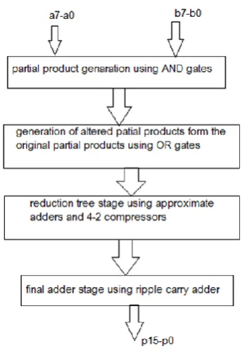
In this modern era, many of the digital systems are error resilient which allows us to take the advantage of approximate computations. This makes the use of replacement of exact computing units by their counterparts. Approximate computing can also decrease the complexity at the designing levels with an increase in performance and power efficiency. Adders and multipliers are the basic buildings blocks of many digital applications. These blocks can be approximated in several ways. Research works are on the rise at many levels on approximate computing. Approximation at designing level is more advantageous as the modifications at this level much easier than the preceding levels.This paper presents a method of designing an approximate multiplier with a modified structure of 4-2 compressor.4-2 compressor is designed with two full adders in general. In this paper these full adders are designed in two methods, i.e., one is by using AVLG(adaptive voltage level at ground) technique with 10transistors, and the second method uses 8 transistors.Outputs from these adders are again fed to a half adder with an x-or gate at its output. This improves the accuracy of compressor. The multiplier is designed using Xilinx in the frontend. And the 4-2 compressor module is also designed in Xilinx on front-end and in backend by using micro wind 3tools.
Keywords: 4-2 compressor, low power multiplier, approximation
I.
Introduction
Need for approximation arises from the fact that exact computation requires more energy. That means wherever the accuracy is not a major concern and the design has to be energy efficient, we may take the advantage of approximation which requires less energy compared to the exact one. For most of the digital circuits adders and multipliers are the basic building blocks. Replacing the exact building blocks with approximate ones results in
energy-efficient designs. A multiplier is a device which multiplies any two operands and gives the corresponding result. Multiplication is nothing but the repeated addition of partial products. This involves the addition of partial products by the use of half adders and full adders based on the bit-size of input operands. Logic gates are used to implement these adder circuits under different
technologies.In the design of high-speed
multipliers, compressors are used in the reduction tree to speed up the process. Basically, these compressors are implemented using full adders. Moreover, Integrated circuit(IC) era of emerging digital trends prefers compact size. This ensures the necessity of area efficient designs for most of the digital circuits. At the same time, it allows the approximate values but not the exact one for the implementation of energy efficient designs. To make the most of error tolerance, various techniques are available. These are of three types: (1) insistent voltage scaling; (2) truncation of bit-width; (3) use of imprecise building blocks.
bound and predictable. This approach can be used for any multiplier regardless of its architecture. Perforation skips the generation of partial products instead of cutting them. Thus decrease the number of operands to be accumulated and reduces delay. An approximate multiplier with configurable partial error recovery is proposed in [5]. This mainly focuses on the mitigation of critical path by using only simple but fast adders in the reduction tree. An inaccurate 4-2 counter is used for error correction in the implementation of multiplier proposed in [6].The existing multiplier[7] proposed two multipliers,one is for approximating all columns, and second one approximates the least significant columns. It is based on the probabilty statistics of the logic block results.This paper presents a new approach for approximate multiplier design using half-adder, full-adder, and 4-2 compressor using different techniques.
II.
Existing work
Existing method evolves the partial products to instigate the terms with different probabilities. These probabilities are analyzed and then approximated in a logical method. Based on probability statistics,actual partial products are accumulated to get generate signals using OR gates. These generate signals have severe impact on error probability.To achieve the exact results, the maximum number of „generate' signals that can be grouped is limited to „4'.Remaining signals other than the „g' signals are accumulated by using the approximate 4-2 compressor, half adder, and full adders.
To reduce the area and delay, the existing method used an OR gate in the place of X-OR for sum in the half adder. This results in one error in sum computation. In case of full adder, X-OR gates are replaced with OR gates in sum calculation.In 4-2 compressor for every three X-OR gates one X-or is replaced with OR gate.This results in 5 wrong cases out of each 16 cases. With these blocks, two multipliers are designed.In first multiplier, the approximation is done in all columns of partial productsof n-bit multiplier. The second multiplier approximation is applied in n-1 least significant OR gates thus reduces the area and power columns. Both the multipliers are designed simple significantly but failed to give accurate values for higher product values
Figure 1 Block diagram of the existing multiplier
Figure.2:Existing multiplier‟s 4-2compressor block
To overcome this, 4-2 compressor module in the existing method is slightly modified in the proposed method. Also the full adder used in the design of compressor is implemented using two techniques. The 4-2 compressor is designed in Xilinx on front-end. It is implemented in backend by using microwind3 and performance is evaluated and the corresponding layouts are obtained.
III.
Proposed work
and „g‟ signals by suitable logic blocks, i.e., half adder, full adder, 4-2 compressor.
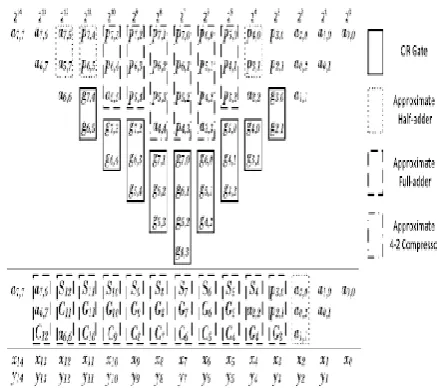
Consider two 8-bit unsigned operands
α=∑7
m=0αm2m; and β=∑7n=0βn2n. Then the partial
products are obtained by performing AND operation between α and β. i.e., am, n=αm.βn.
Resultant partial products are as shown in below figure 2. The partial products am,n and an,m in the
columns containing more than three partial
products are combined to get propagate and
generate signals as shown. These form the altered partial products pm,n and gm,n. These are obtained as
follows:
Pm,n = am,n + an,m
Gm,n= am,n. an,m
The reduction tree for obtaining partial products is shown in below figure.3:
Fig.3. altered partial products formed by propagate and generate signals.
In the process of approximating the altered partial products, "generate" signals are accumulated column-wise using OR gates.OR gates used for a column having mgenerate signals is m/4.
Partial products other than the generate signals are approximated using half adder,full adder and 4-2 compressor. In the proposed method approximate half adder and full adder blocks are designed using Adaptive Voltage Level technique which is used to reduce the power consumption. In general, the 4-2 compressor is designed using two full adders. To improve the accuracy, the proposed method includes a half adder with an XOR gate at the output. Block diagram of the proposed 4-2 compressor is shown in figure.5:
Figure 4:Logic blocks used for approximation of altered partial products
Figure5: proposed 4-2 compressor block diagram
Two full adders are used for input, X1,X2
Adaptive voltage scaling is a closed-loop dynamic power reduction technique based on the actual operating conditions of the chip. During run-time the power is adjusted continuously to eliminate the excess margins. As the smaller feature size allows more functions to be implemented in the same area, there is an upturn in current density and the associated power dissipation. Supply voltage reduction technique is one of the best way to be used, as the direct consequence of static voltage scaling is the performance degradation.Generally two types of AVL techniques are used.
AVL at source(AVLS) uses a control circuit at the supply voltage, i.e., upper end to undermine the supply voltage whenever required. Adaptive voltage level at Ground(AVLG) uses control circuit at the ground, i.e., lower end to lift the ground potential when the required voltage level is not available.
This technique uses a combination of 1nmos &2pmos circuits are parallelly connected. An input clock pulse is applied at the nmos in AVLG and all the pmos are connected to ground. This would lift the ground potential to the required level to reduce the power consumption. Any defects in half adder during power consumption can be eliminated by the use of clock at the input.
Conventional cmos requires a total of 16 transistors for the implementation of halfadder because the design is based on transmission gate and XOR/XNOR.AVLG technique makes it possible to design a half adder with only 6 transistors. As the number of transistors required is much reduced,the power consumption will be low.
One of the major buliding blocks of digital design is the full adder.Generally, 28 transistors are required for a conventional CMOS full adder
implementation.But our proposed method requires only 8 transistors.
Its basic circuit comprises of 2-XORgates for implementing sum and a 2input multiplexer for carry output implementation. Two input multiplexer using pass gate transistor logic is used here.It can be obtained by connecting PMOS &NMOS along with SEL line as in MUX.For an active low signal,PMOS works and for active high signal,NMOS works.When the SEL line is 0, PMOS conducts and NMOS stands idle.For SEL is 1,NMOS is ON,PMOS is off.Thus its acts like a 2to1 multiplexer.Each x-or gate requires three transistors.Totally full adder design requires two xor gates and one mux.Thus, it can be formed by using 8 transistors only.
IV.
Simulation results
Proposed multiplier design with the modified 4-2 compressor is simulated using Xilinx tool on the front end. The results obtained are as ahown below:
Figure.6:Top view of multiplier
Figure.7: simulation result of proposed multiplier
Figure.8: 4-2 compressor top view
Figure.9: 4-2 compressor rtl view
Figure.10: Simulation result of modified 4-2 compressor
Here, ends the front-end designing of multiplier and the 4-2 compressor.
4-2 compressor module is designed at
back-end using microwind3 with 65nm
technology.It is implemented in two methods. In the first method, the full adder is designed using AVLG technique with 10 transistors. Even though it gives exact results for sum in all the cases, carry is wrong in most cases.As an endeavour to modify the carry error cases, second method is designed with 8transistors. This gives the carry error for
3cases which is somewhat better than the compressor with 10 transistor full adder. These circuits are implemented in microwind and the layouts are obtained. Voltage-current and voltage-frequency plots are observed. Simulation result of the proposed circuit using dsch tool is shown in below figure.11:
Figure.11: simulation result for compressor
Wrongoutputs for sum in some cases and wrong carry outputs in 3 cases due to power consumption in analog circuit paths. When converting analog voltage to digital „0‟ or digital‟1‟, analog voltage must reach the upper voltage level for logic‟1‟ and the lower voltage level for logic‟0‟ which are already set. Practically it is not possible to get the exact voltages on the circuit path as there may be leakage or unexpected power consumptions.
V.
Conclusion
Proposed multiplier increases the accuracy level so that it can multiply any number up to the range of 14x13. It is highly efficient, consumes less power and area efficient as the number of transistors used is reduced compared to that of previous works.Adaptive voltage level at ground reduces the power consumption by lifting-up the ground potential whenever required and decreasing
the voltage through transistors whenever
REFERENCES
[1] V. Gupta, D. Mohapatra, A. Raghunathan, and K. Roy, “Low-power digital signal processing using approximate adders,” IEEE Trans. Comput. Aided Design Integr. Circuits Syst., vol. 32, no.1, pp.124–137, Jan.2013.
[2]A.Momeni, J. Han, P.Montuschi, and
F.Lombardi, “Design and analysis of approximate
compressors for multiplication,” IEEE
Trans.Comput., vol. 64, no. 4, pp. 984–994, Apr. 2015.
[3]S.Narayanamoorthy, H.A.Moghaddam, Z.Liu,
T.Park, and N.S.Kim, “Energy-efficient
approximate multiplication for digital signal processing and classification applications,” IEEE Trans. Very Large ScaleIntegr. (VLSI) Syst., vol. 23, no. 6, pp. 1180–1184, Jun. 2015.
[4]G.Zervakis, K. Tsoumanis, S. Xydis, D. Soudris, and K. Pekmestzi, “Design-efficient approximate multiplication circuits through partial product perforation,” IEEE Trans. Very Large Scale Integr. (VLSI) Syst.,
vol. 24, no. 10, pp. 3105–3117, Oct. 2016.
[5]C. Liu, J. Han, and F. Lombardi, “A low-power, high-performance approximate multiplier with configurable partial error recovery,” in Proc.Conf. Exhibit. (DATE), 2014, pp. 1–4.
[6]C.H.Lin and C.Lin, “High accuracy approximate multiplier with error correction,” in Proc. IEEE 31st Int. Conf. Comput. Design, Sep. 2013, pp. 33– 38.
[7]Suganthivenkatachalam and seok-bum KO, senior member IEEE. “Design of power and area
efficient approximate multipliers” IEEE
transactions on VLSI systems.2017
[8]MateshwarSingh, Surya deoChoudhary,
Asutoshkr.singh, “Design and simulation of half adder circuit using AVL technique based on CMOS technology” IRJET august 2017
[9]Bishwarupmukherjee, BiplapRoy,