Estimation of the Ageing of Metallic Layers in Power
Semiconductor Modules Using the Eddy Current
Method and Artificial Neural Networks
Tien A. Nguyen1, Pierre-Yves Joubert2, *, and St´ephane Lefebvre1
Abstract—In high power operations, the ageing of power semiconductor modules has been often observed by several failures due to high temperature cycling. The main failures may be metallization reconstruction, solder delaminations, bond wire lift-offs or bond wire heel crackings, conchoidal breaking of ceramics. The paper focuses on the non-contact monitoring of the ageing of the aluminum metallization top layer and of the solder bottom layer of a power die, using the eddy current method. The ageing is assumed to induce a decrease of these layers conductivity. The evaluation of both layers conductivity changes are estimated using artificial neural networks starting from eddy current data provided by finite element computations carried out in the case of several aged die configurations. The error of estimation is less than a few percent in the considered cases and it demonstrates the relevance of the eddy current method to monitor the ageing state of power modules. The proposed approach provides relevant results which will be validated on experimental data in future works.
1. INTRODUCTION
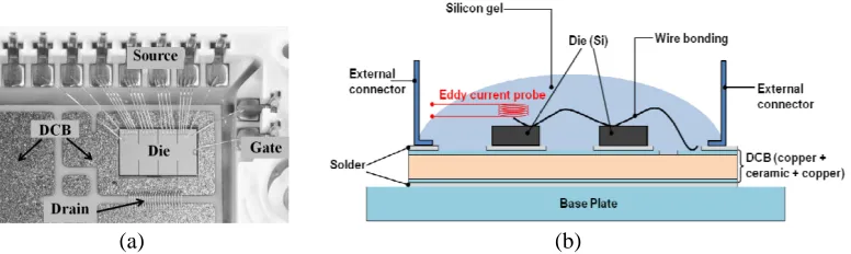
Electronic power modules are widely used for energy processing purposes, and their development extends to more and more industrial domains, such as automotive or aeronautics, with increasing demands in terms of reliability. Standard power modules are constituted of semiconductor dies soldered on direct copper bonded (DCB) ceramic substrate, as shown in Figure 1. Inside power modules, electrical connections are made by soldering or wire bonding between metallized layers. In addition, the DCB is implanted on a metallic base plate used as a mechanical support as well as a thermal cooler. The upper side of the modules is covered with an insulating silicone gel used to avoid partial discharges within the module. As a result, these modules are constituted of stacks of materials of various natures featured by various electro-mechanical properties. They include semiconductors, electrically conductive materials (metallic layers, solder layers. . .), and insulators (silicone gels, ceramics).
In many applications, power modules have to operate within variations of the ambient temperature, referred as passive temperature cycles [1, 2], which may reach high amplitudes. For instance, the environment temperature may rise to 120◦C in the automotive application, or even to 200◦C in the vicinity of aircraft jet engines. Furthermore, power modules are submitted to so-called active temperature cycles, which are relative to temperature variations resulting from their own power dissipation [1, 2]. Due to the different thermal expansion coefficients of the materials constituting the power modules, the thermal cycles induce mechanical stresses which may result in various types of degradations, such as solder delaminations, bond wire lift-offs and heel cracking, ceramics conchoidal fractures, or metallization reconstruction [1–6].
Received 16 September 2014, Accepted 17 October 2014, Scheduled 19 December 2014 * Corresponding author: Pierre-Yves Joubert ([email protected]).
(a) (b)
Figure 1. Multilayered conductive structure of power semiconductor module, (a) top view of a typical module, (b) schematic cut view.
Therefore, the analysis and evaluation of the degradation process is a key issue for optimizing the use of power modules as well as for preventing failures. In particular, the degradation of the metallized layers of chips has been highlighted by many authors as a major source of failure [1, 2, 6]. As a result, the non-destructive evaluation (NDE) of such layers may help to better understand the alteration process, and subsequently, to foresee and prevent failures.
The eddy current (EC) method allows the quantitative NDE of metallic layers to be carried out [7], and hence, it is a good candidate to evaluate the ageing state of chip metallization and solder layers. Furthermore, the method is easy to implement, non contact, robust, and suitable to in situ NDE applications, providing EC micro-sensors [8] are considered. Previous works carried out by the authors have shown that EC methods can quantitatively diagnose the state of thermally-aged 4µm aluminum single layers deposited on a silicon bulk [9]. The same authors have also experimentally highlighted that the EC technique implemented in a wide frequency range was relevant to qualitatively sense the ageing state of different conducting layers in an actual power module sample [10].
In this study, the authors aim at assessing the feasibility of the quantitative EC NDE of the ageing state of multiple conductive layers of an aged power module die. To do so, a typical transistor chip soldered on a DCB substrate is considered. For this chip, the alteration of the upper aluminum metallization and the bottom-side soldering layer are jointly considered. Since it is difficult to obtain module samples featuring such layers of adjustable ageing state, data only provided by finite element (FE) computations are considered in this study. In order to evaluate the feasibility of the method, computed data relative to the interactions between a mini-cup-core bobbin-coil EC sensor and a transistor featured by adjustable ageing parameters are used. Parametric computations enable data relative to various ageing states to be provided. These data are firstly used to analyze and evaluate the sensitivity of the EC method to multiple layer alterations. They are used secondly to feed an artificial neural network (ANN) [11] so as to elaborate an able estimator to evaluate the ageing parameters of the considered transistor layers, starting from the available EC data. In the second section of this paper, the considered transistor sample and the implemented EC method are presented. Then, the implementation of the FE computations is described and obtained results are discussed. In Section 3, the elaboration of the used ANN and the estimation of transistor ageing state using the ANN are addressed. Conclusions are presented in Section 4.
2. IMPLEMENTATION OF THE EC NDE OF AN AGED TRANSISTOR CHIP
2.1. Basic Principles of the EC Method Used
distance (lift-off) and on the properties of the part. These parameters may be sensed through the impedance changes measured at the ends of coil. The EC data used in this study are the complex normalized impedanceZn of the probe, which can be expressed as [12]:
Zn=Rn+jXn= R−XR0
0
+jX
X0
(1)
where R0 and X0 are the resistance and the reactance of the uncoupled probe respectively, and R and X are respectively the resistance and the reactance of the complex impedance of the probe when coupled to the test part. The use of Zn is more relevant than the use of the impedanceZ =R+jX
of the coupled probe because it enables getting rid of the influence of the constitution of the probe (losses R0 and self reactance X0 of the coil winding [12]) to focus on the impedance changes due to the tested part. Indeed, the normalized impedance Zn only depends on the used excitation frequency,
the electromagnetic properties (electrical conductivity σ, magnetic permeability) and the geometric properties of the part (sensor lift-off, layer thickness) [13].
In the case of large massive metallic parts of known thickness, it has been established that the normalized impedance of the sensor coupled to the part may be expressed using a simple analytical coupling model based on the analogy to an electrical transformer [12, 13]. This model enables to foresee the frequency responses of Zn according to the geometric and electromagnetic properties of
the investigated material. It also allows the universal impedance diagram (UID), which is the evolution ofZnplotted in the (Rn,Xn) complex plane, to be plotted for frequencies ranging from 0 to infinity [12]. For massive plane parts, the UIDs feature expected patterns. In practice, these expected patterns can be used to estimate the part parameters starting from EC data provided in adequate frequency bands. In the case of a thin aluminum film deposited on a silicon substrate, the authors have shown in [9] that the ageing state of the thin film may be quantified starting from the alterations of the UID resulting from the modifications of its conductivity with thermal fatigue. Moreover, the authors have experimentally pointed out that the frequency response Zn of a commercial EC sensor being implemented in the
5 Hz–2.5 MHz bandwidth was relevant to sense the ageing of metallic layers in power semiconductor module [10]. Indeed, at low frequencies, the obtained EC data were found to be sensitive to the ageing state of the solder layer and the DCB substrate of the power module. Conversely, at high frequencies, due to skin effect in the metallic layers [7], the EC data were found to be mainly related to the power module chip, and more specifically to the metallized top layer of the chip [10]. However, these preliminary experimental results only enable to assess the effects of the metallization ageing. The actual ageing state evaluation requires one i) to develop an accurate modeling tool of the interactions between the EC probe/power module [14, 15] and ii) to solve the inverse problem so as to estimate the value of the metallization conductivity starting from the collected EC data.
In order to assess the feasibility of the quantitative EC estimation of the ageing state of multiple conducting layers of the die, in this study the authors have chosen to turn to FE modeling to provide EC data related to multilayer aged specimens. The implementation of such FE computations is presented in the following subsection.
2.2. Simulation of Electromagnetic Coupling between EC Probe and Power Semiconductor
In this section, finite element (FE) computations of the EC testing of a typical power module transistor chip are reported. To do so, a cup-core bobbin coil sensor (NORTEC†3551F-1 MHz) commercialized by NORTEC is considered. The coils have an effective sensitive area of approximately 2 mm in diameter. The preferred frequency range is from 1 MHz to 2 MHz.
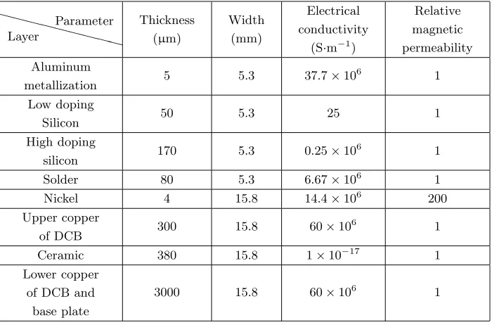
Assuming that the used EC sensor is of sufficiently small radius comparatively to the transistor chip surface (6.59×10.52 mm2), the whole simulation workspace may be considered as being axisymmetric. Therefore two-dimensional (2D) electromagnetic computations are carried out using 2D ANSYS‡ software. A standard power semiconductor module consists of a silicon die, a DCB substrate, and a base plate. The silicon die is made of a thin aluminum metallization layer, a low doping silicon layer
(epitaxial layer), and a high doping silicon layer (substrate). The die is soldered to the DCB substrate. The resultant solder layer is around 80µm. The dimensions and constitutive parameters of each layer have been chosen as close as possible to the ones of a typical power module (e.g., MOSFET module fabricated by Microsemi [10]). Dimensions and features are gathered in Table 1 and the corresponding computational axisymmetric workspace is depicted in Figure 2.
In order to implement the FE computations, a quasi static analysis is used featuring FE element PLANE13 in the ANSYS software. The harmonic model uses the magnetic vector potential formulation to solve the eddy current region and each node of the elements owns a magnetic vector potential as degree of freedom. Here we chose a quadrilateral element featuring 4 nodes in rotational axisymmetry (Figure 2).
Magnetic boundary conditions are applied to the exterior boundaries of the workspace. TheY axis
Figure 2. Simulation of multilayered structure of power semiconductor module.
Table 1. Dimensions and physical parameters of layers in the simulated structure.
XXXXXXXXX
Layer
Parameter Thickness
(µm)
Width (mm)
Electrical conductivity
(S·m−1)
Relative magnetic permeability
Aluminum
metallization 5 5.3 37.7×10
6 1
Low doping
Silicon 50 5.3 25 1
High doping
silicon 170 5.3 0.25×10
6 1
Solder 80 5.3 6.67×10⁶ 1
Nickel 4 15.8 14.4×10⁶ 200
Upper copper
of DCB 300 15.8 60×10
6 1
Ceramic 380 15.8 1×10⁻¹⁷ 1
Lower copper of DCB and
base plate
represents the rotational symmetry axis. The parallel flux condition is applied to this axis. Also, the open boundaries are set to parallel flux conditions. Figure 2 shows the magnetic flux parallel condition at they-axis of the model and at the open boundaries.
The procedure of data extraction will be described below. The FE computation allows simulating the magnetic flux (ψ) going through the sensor core. The electromotive force (EMF) induced at the ends of the sensor coil is calculated as follows:
EMF=j·2·π·f·ψ (2)
wheref is the excitation frequency,j is the imaginary unit.
Then the impedanceZ of the sensor (Z =R+j·X) is determined with the expression given by:
Z = EMF
I (3)
whereI is the excitation current.
The normalized impedance (Zn) is then computed using Eq. (1) after FE computations of the sensor in unloaded and loaded configurations.
In the considered FE workspace, the material parameters which are modified by the ageing process are the electrical conductivity of both the power die aluminum layer and the solder layer between the power die and the DCB subtract. For the initial state of the power module, the aluminum conductivity
σal0 has been set to the value of bulk aluminum, i.e., σ0al = 37.7 MS·m−1. In the same way, the solder conductivityσ0
solder at initial state is set to be equal to the conductivity of Sn63Pb37alloy, widely used in the standard power modules, i.e.,σ0solder = 6.67 MS·m−1. Then, the ageing of both layers are simulated by decreasing the conductivity of these layers. The reduction factors are denotedαal andαsolder for the aluminum and solder layers, respectively. They are such that:
σal= σ
0 al αal
σsolder = σ 0 solder αsolder
(4)
In this study,αalranges from 1 to 19, andαsolder ranges from 1 to 11, these values being estimated to be realistic, considering previous experimental evaluations [9, 10]. These variations lead to a large set of possible ageing configurations. Figure 3 provides some examples of UID computed in the 5 Hz–2.5 MHz bandwidth for sound and aged configurations.
0 0.02 0.04 0.06 0.08 0.1 0.12 normalized resistance (R )n
α al = 1, α solder= 1
α al = 19, α solder = 1
α al = 1, α solder = 11
α al = 19, α solder = 11
2.5 MHz
2.5
MHz MHz2.5
2.5 MHz 5 Hz
0.8 0.85 0.9 0.95 1 1.05
normalized reactance
(X
)
n
In Figure 3 the initial state (αal = 1, αsolder = 1), two intermediate ageing states (αal = 1, αsolder = 11), (αal = 19, αsolder = 1), and the most advanced ageing state (αal = 19, αsolder = 11) are considered. The UID obtained of the most considerable ageing state has the smallest local radius at low frequencies and the shortest length, the UID featuring the smallest radius at high frequencies corresponds to the ageing state of only conductivity variation of aluminum layer (αal = 19,αsolder = 1), and the UID corresponding the only conductivity variation of solder layer (αal = 1, αsolder = 11) has the greatest radius at high frequencies. It isn’t easy to claim the behavior change of UID in the case of the ageing state of both these layers jointed. However, theoretically, we can note that the low frequency part of UID is mainly related to the solder and substrate layers, and that the high frequency part of UID is mainly related to the die. Indeed, at high frequencies, the EC induced in the substrate are strongly reduced by the aluminum and solder layers which are highly conductive. This is why the substrate is hardly sensed by the E probe at these frequencies. From these examples, one may conclude that a relevant frequency band may be determined to select EC data for ageing evaluation purposes.
2.3. EC Data for the Estimation of Ageing
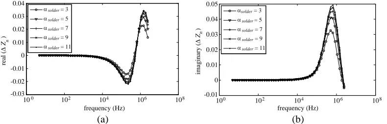
In order to estimate the conductivity variations of the power die aluminum and solder layers, the variations of the normalized impedance between the ageing state and the initial state, denoted ΔZn is
defined as:
ΔZn=Zn(αal, αsolder)−Zn
α0al, α0solder
(5)
whereZn(α0al, α0solder) =Zn(1,1) is the normalized impedance obtained at initial state.
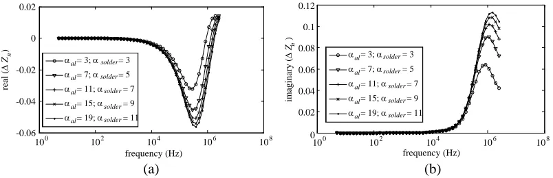
The variations of the real and imaginary parts of ΔZn(f) versus frequency are presented in Figures 4
100 102 104 106 108
-0.03 -0.025 -0.02 -0.015 -0.01 -0.005 0 Frequency (Hz) real ( Δ Z ) n
αal = 3 αal = 5 αal = 7 αal = 9 αal = 13 αal = 19
100 102 104 106 108
0 0.01 0.02 0.03 0.04 0.05 0.06 frequency (Hz) imaginary ( Δ Z ) n
αal = 3 αal = 5 αal = 7 αal = 9 αal = 13 αal = 19
(a) (b)
Figure 4. ΔZn as a function of the excitation frequency for several values of the conductivity of the aluminum layer, the solder conductivity being fixed at the initial state, (a) real part of ΔZn, (b) imaginary part of ΔZn.
100 102 104 106 108
-0.03 -0.02 -0.01 0 0.01 0.02 0.03 0.04 frequency (Hz)
αsolder = 3 αsolder = 5 αsolder = 7 αsolder = 9 αsolder = 11
100 102 104 106 108
-0.01 0 0.01 0.02 0.03 0.04 0.05 frequency (Hz)
αsolder = 3 αsolder= 5 αsolder = 7 αsolder = 9 αsolder = 11
real ( Δ Z ) n imaginary ( Δ Z ) n (a) (b)
Figure 5. ΔZn as a function of the excitation frequency for several values of the solder conductivity,
100 102 104 106 108 frequency (Hz)
α al = 3; α solder= 3
α = 7; al α = 5solder
α al = 11; α solder = 7
α al = 15; α solder = 9
α al = 19; α = 11 solder
100 102 104 106 108
frequency (Hz)
α al = 3; α solder = 3
α = 7; al α solder = 5
α al = 11; α solder = 7
α al = 15; α solder = 9
α = 19; al α solder = 11
real (
Δ
Z
)n
imaginary (
Δ
Z
)
n
(a) (b)
-0.06 -0.04 -0.02 0 0.02
0 0.02 0.04 0.06 0.08 0.1 0.12
Figure 6. ΔZn as a function of the excitation frequency for several values of the aluminum layer
conductivity and of the solder layer conductivity, (a) real part of ΔZn, (b) imaginary part of ΔZn.
to 6 for various ageing configurations. Figure 4 illustrates the influence of the aluminum conductivity (σal) on the variations of ΔZn(f), the aluminum layer is successively altered by six attenuation
values αal = [3, 5,7,9,13,19], while the solder conductivity is fixed at initial state (αal = 1). In
the same manner, Figure 5 illustrates the influence of the solder layer conductivity, σsolder (with αsolder = [3,5, 7,9,11]) on the variations of ΔZn(f), the aluminum conductivity is fixed at initial state (αal = 1). Finally, Figure 6 shows the influence of both conductivity variations on ΔZn(f) for
(αal, αsolder) taking values such as (3, 3); (7, 5); (11, 7); (15, 9); and (19, 11). These graphs point out that there exists a relevant frequency band which enhances the sensitivity of the EC sensor to the conductivity changes. In what follows, the frequency band (FB) used for estimation purposes is set to
FB = [11.8 kHz–2.5 MHz].
In addition, noisy EC data are considered in this study. Indeed, based on previous experiments [10], EC data measured with the NORTEC sensor on such a power module structure feature a signal to noise ratio (SNR) close to 60 dB. So as to be more realistic in this study, computed EC data have been altered by additive white noise standing for so electronic noise as well as measurement uncertainties such as sensor positioning repeatability [16]. This additive noise is added in equal proportion to both the real and the imaginary parts of ΔZn so that [17]:
SNR= 20×log10
⎛
⎝max|ΔZn|
λ2
real +λ2imag
⎞
⎠ (6)
whereλreal and λimag are the standard deviations of the noise altering the real and imaginary parts of ΔZn, respectively. Starting from these noisy EC data, the evaluation of the conductivity variations of
aluminum and solder layer using artificial neural network is implemented in the following section.
3. EVALUATION OF CONDUCTIVITY VARIATION OF ALUMINUM AND SOLDER LAYER USING ARTIFICIAL NEURAL NETWORK
The goal of this study is to estimate the variations of the aluminum conductivity (σal) and solder
conductivity (σsolder) during the ageing process. In order to bypass the difficulties of inverting a numerical model to estimate these parameters starting from EC data [18], a model-free estimation technique based on the use of an ANN is considered. This kind of approach has been proven to be efficient in various modeling and estimation problems in the electromagnetic domain [19, 20]. In this study, a feed-forward neural network (FFNN) is implemented to estimate the conductivity variations [21]. This particular ANN was found relevant in several eddy current estimation problems [22, 23]. In this paper, the authors use the neural network toolbox of Matlab to implement the FFNN estimation [24].
according to the estimation errors observed in known configurations. The validation database is used to measure network generalization ability and to halt training process when generalization stops improving. The testing database has no effect on the training. It is used to provide an estimation of the network performances during and after training [24].
3.1. Elaboration of the FFNN for Estimating Conductivity Variations
The inputs of FFNN consist of the multi-frequency EC data ΔZn obtained in various configurations of aged module. For each selected configuration, 21 different values of ΔZn obtained for 21 frequencies logarithmically distributed in the frequency bandFB, are considered.
Since the real and the imaginary parts of ΔZn are separately considered, the FFNN is fed with a total amount of 42 inputs. The FFNN features two outputs, the estimated conductivity of the aluminum layer (ˆσal) and the estimated conductivity of the solder layer (ˆσsolder). The used FFNN is finally set with a single hidden layer, as depicted in Figure 7.
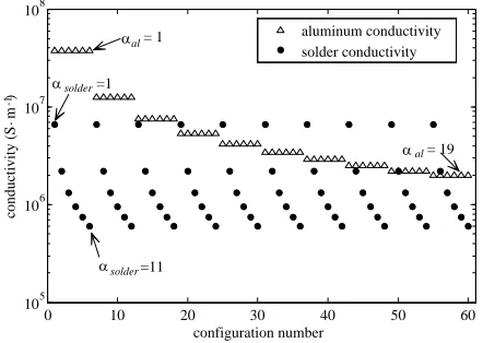
Among the EC data provided by FE computations, the training and validation database has been created from the normalized impedance variations (ΔZn) of sixty configurations of ageing states.
These sixty configurations correspond to the ten values of aluminum conductivity in the range of
αal = [1,3,5, . . . , 19] given by the odd factors of αal, and the six values of solder conductivity in
the range of αsolder = [1,3,5, . . . , 11] given by the odd factors of αsolder. Figure 8 illustrates these sixty configurations of ageing state selected in the first data set (training and validation process). Then we will chose the second data set (testing database) of ageing states which are different from the ageing states of the training and validation databases. The testing database has been made from ΔZn values for nine configurations of ageing state which correspond to three values of aluminum conductivity in the range of αal = [8,10,12] given by the even factors ofαal and three values of solder conductivity in the range of αsolder = [4,6, 8] given by the even factors of αsolder. The testing databases allow us to calculate the estimation error of each built ANN.
After adding the noise to the EC data, each value of ΔZn will be multiplied byM different values
(M = 30) around ΔZnwhich ensures the signal-noise-ratio (SNR)of 60 dB as defined in the Section 2.3.
For the training and validation databases, the total number of input-output couples of EC data is equal to 60×30 = 1800. For the testing database, the total number of input-output couples is equal to 9×30 = 270. Each input-output couple of EC data is featured by 42 inputs consisting of the real and imaginary part of ΔZn and 2 outputs relative to the actual values of conductivitiesσal andσsolder.
Because the neural network minimization problem is often ill-conditioned, the ANN training process uses the back propagation Levenberg-Marquardt algorithm [25, 26], and its generalization ability was assessed according to a cross-validation procedure [27].
Figure 7. Fully connected feed-forward ANN with one hidden layer and one output layer used for the estimating the conductivity variation.
0 10 20 30 40 50 60
105 106 107 108
configuration number
conductivity (S m )
-1
aluminum conductivity solder conductivity al = 1
solder=1
solder=11
al = 19
.
α
α
α
α
To do so, among 1800 input-output couples of the training and validation database, 1/6 of the data corresponding to the ageing states located in the limits of ageing (αal = 1 and αal = 19) have
been dedicated to the validation process of ANN, the remaining data being dedicated to the training process of the ANN. In order to search for an optimized ANN we consider ANNs having the number of neurons in the hidden layer varying from 1 to 80. Then we select the network corresponding to the lowest estimation error. Using the testing database, the root mean square error (RMSE) between the estimated conductivities (ˆσal and ˆσsolder) and the actual conductivities (σal and σsolder) have been calculated for every network using:
RMSE =
1
N ×
N
i=1
⎛
⎝ 1
M ×
M
j=1
(ˆσij −σ)2
⎞
⎠ (7)
where M is the number of generated values simulating the added noise, M = 30, N is the number of configurations of ageing state, N = 9 with the testing database of the second data set.
Figure 9 shows the evolution ofRMSE of ˆσal and ˆσsolder calculated from the testing database as a function of number of neuron in the hidden layer. We can note that a hidden layer featuring 56 neurons is a good choice to keep the evaluation error as low as possible for the estimation ofσal and σsolder.
3.2. Estimation Results
Joint estimation of aluminum conductivity and solder conductivity has been performed by mean of the ANN selected in Section 3.1. In order to test the generalization capability of the chosen network, the testing database has been enlarged by the different ageing states that are located outside of the training and validation database. Now the new testing database corresponds to six values of aluminum conductivity in the range of αal = [8,10,12,14,16,18] and three values of solder conductivity in the range of αsolder = [4,6,8]. As a result, the new testing database is constituted of 18 ageing state configurations. The chosen frequency band and the noise power added to the EC data were the same as previously described. In order to quantify the estimation results, we define the estimate bias (μ) as the mean value of the estimated conductivity. The mean and the standard deviation of the values of the estimated conductivity (std) for M estimated values of each ageing configuration are given by:
μ = 1
M ×
M
k=1
ˆ
σk (8)
0 10 20 30 40 50 60 70 80
103 104 105 106 107
neuron number of hidden layer
RMSE (S m )
-1
RMSE of estimated aluminum conductivity RMSE of estimated solder conductivity
.
Figure 9. Generalization of ANN for selecting the optimal network of estimation.
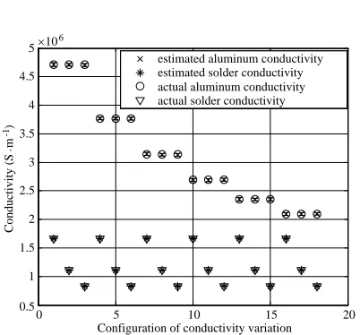
0 5 10 15 20
×106
Configuration of conductivity variation estimated aluminum conductivity estimated solder conductivity actual aluminum conductivity actual solder conductivity
0.5 1 1.5 2 2.5 3 3.5 4 4.5 5
Conductivity (S m )
-1
.
std =
1
M−1 ×
M
k=1
(ˆσk−μ)2 (9)
where σ and ˆσ represent the considered conductivity σal and σsolder (true values) and its estimation respectively. M is still defined as the number of generated values simulating the added noise,M = 30. Figure 10 illustrates all ageing configurations of the new testing database corresponding to the actual conductivities (σal and σsolder) and the estimated ones (ˆσal and ˆσsolder). The estimated conductivities are represented by their mean values μ (Eq. (8)) with the error bar being equal to the standard deviation, std (Eq. (9)). One can note that the estimations are satisfactory with the very small deviations between the estimated and actual values of the conductivities.
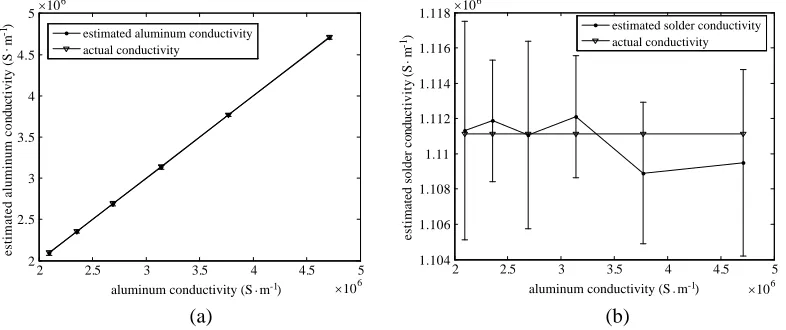
Figures 11 to 13 represent the conductivity estimation when the solder conductivity has been fixed at the value corresponding to the factors ofαsolder = 4,6,8 respectively and the aluminum conductivity is the value of new testing data corresponding to the factor of αal = [8,10,12, 14,16,18]. The solid
lines represented on these figures link the points corresponding to the estimate bias (Eq. (8)) and the error bars plotted around these points show the estimation standard deviation (Eq. (9)). The dashed
2 2.5 3 3.5 4 4.5 5
×10 6 2 2.5 3 3.5 4 4.5
5×10 6
aluminum conductivity (S m )-1
estimated aluminum conductivity (S m )
-1 estimated aluminum conductivity
actual conductivity
2 2.5 3 3.5 4 4.5 5
×106 1.658 1.66 1.662 1.664 1.666 1.668 1.67 1.672×10
6
aluminum conductivity (S m )-1
estimated solder conductivity (S m )
-1
estimated solder conductivity actual conductivity . . . . (a) (b)
Figure 11. Results of joint estimation ofσal andσsolder forαal = [8,10,12, 14,16,18] andαsolder = 4, (a) estimation of aluminum conductivity, (b) estimation of solder conductivity. (The error bar corresponds to the standard deviation, centered on the estimate biasμ).
2 2.5 3 3.5 4 4.5 5
2 2.5 3 3.5 4 4.5
5×10 6 est im ated alumin u m co nduct iv it y ( S m )
-1 estimated aluminum conductivity
actual conductivity
2 2.5 3 3.5 4 4.5 5
×10 6 1.104 1.106 1.108 1.11 1.112 1.114 1.116 1.118×10
6 e st imated solde r c o n d u ctivity ( S m ) -1
estimated solder conductivity actual conductivity
.
.
(a) (b)
×10 6
aluminum conductivity (S m ). -1 aluminum conductivity (S m ). -1
2 2.5 3 3.5 4 4.5 5 2
2.5 3 3.5 4 4.5
5×10 6
estimated aluminum conductivity (S m )
-1
estimated aluminum conductivity actual conductivity
2 2.5 3 3.5 4 4.5 5
8.24 8.26 8.28 8.3 8.32 8.34 8.36 8.38×10
5
estimated solder conductivity (S m )
-1
estimated solder conductivity actual conductivity
.
.
×10 6
(a) (b)
×10 6
aluminum conductivity (S m ). -1 aluminum conductivity (S m ). -1
Figure 13. Results of joint estimation ofσal andσsolder forαal = [8,10,12, 14,16,18] andαsolder = 8, (a) estimation of aluminum conductivity, (b) estimation of solder conductivity. (The error bar corresponds to the standard deviation, centered on the estimate biasμ).
Figure 14. Histogram of estimation error for the aluminum conductivity.
Figure 15. Histogram of estimation error for the solder conductivity.
lines link the points corresponding to the actual conductivities.
In addition, Figure 14 and Figure 15 illustrate the histogram of estimation errors. The error of estimation is calculated for all 540 input-output couples of the new testing data, the error of estimation being given by the following expression:
error = 100%×σˆ−σ
σ (10)
where ˆσ and σ are the estimated conductivity and the actual conductivity, respectively.
in the aluminum layer, the maximal frequency should be increased so that at high frequencies, the influence of the solder layer would be negligible. In Figure 15, we note that the most aged configuration of the solder layer corresponding to the lowest conductivity provides the highest error of estimation. This may be due to the fact that because of the decrease of solder conductivity, the electromagnetic interaction between the EC probe and the solder layer becomes weaker, thus EC data is less sensitive to the solder layer of lower conductivity. In this case, to improve the results of estimation in the solder layer, the minimal frequency of investigation should be decreased.
Thus, the results of estimation show that by exploiting the simulated EC data featuring noise corresponding to a 60 dB SNR, we can estimate the evolution of ageing state of both aluminum and solder layers using an ANN. These preliminary results are very encouraging and invite us to apply this method to data provided by the experiment on actual power module samples.
4. CONCLUSIONS AND PERSPECTIVES
The paper focuses on the estimation of conductivity variation in the multilayered structure of a power semiconductor module using the EC method during an ageing process. The authors have used the ANN to estimate the conductivity variations of the aluminum and the solder layers in the power module by exploiting the simulation data of electromagnetic coupling between the EC probe and the multilayered structure of power module. The data used on this study are simulated EC data provided by FE computations. They are computed for different ageing configurations corresponding to conductivity changes appearing in two metallic layers (aluminum and solder). The results indicate that the implemented ANN allows estimating the conductivity of aluminum layer and solder layer with an estimation error less than 4%. The study demonstrates that the EC method is relevant for the estimation of the ageing state of power modules.
Further research will focus on the experimental validation of the methods. Once the variation of aluminum and solder conductivity are validated on a real power semiconductor module, the development of integrated EC systems dedicated to the health monitoring of power electronic components will be envisaged.
REFERENCES
1. Lutz, J., T. Hermann, M. Feller, R. Bayerer, T. Licht, and R. Amro, “Power cycling induced failure mechanisms in the viewpoint of rough temperature environment,” Proceedings of the 5th
International Conference on Integrated Power Electronic Systems, 55–58, Nuremberg, Mar. 2008.
2. Ciappa, M., “Selected failure mechanisms of modern power modules,” Microelectronics Reliability, Vol. 42, Nos. 4–5, 653–667, 2002.
3. Martineau, D., T. Mazeaud, M. Legros, P. Dupuy, C. Levade, and G. Vanderschaeve, “Characterization of ageing failures on power MOSFET devices by electron and ion microscopies,”
Microelectronics Reliability, Vol. 49, Nos. 9–11, 1330–1333, 2009.
4. Detzel, T., M. Glavanovics, and K. Weber, “Analysis of wire bond and metallisation degradation mechanisms in DMOS power transistors stressed under thermal overload conditions,”
Microelectronics Reliability, Vol. 44, Nos. 9–11, 1485–1490, 2004.
5. Smet, V., F. Forest, J. Huselestein, A. Rashed, and F. Richardeau, “Evaluation ofVCE monitoring as a real time method to estimate ageing of bon wire — IGBT modules Stressed by power cycling,”
IEEE Transactions on Industrial Electronics, Vol. 60, No. 7, 2760–2770, 2013.
6. Pietranico, S., S. Lefebvre, S. Pommier, and M. Berkani Bouaroudj, “A study of the effect of degradation of the aluminum metallization layer in the case of power semiconductor devices,”
Microelectronics Reliability, Vol. 51, Nos. 9–11, 1824–1829, 2011.
7. Udpa, S. and P. Moore, Nondestructive Testing Handbook, 3rd Edition, Vol. 5, Electromagnetic Testing, The American Society for Nondestructive Testing, 2004.
9. Nguyen, T. A., P.-Y. Joubert, S. Lefebvre, G. Chaplier, and L. Rousseau, “Study for the non-contact characterization of metallization ageing of power electronic semiconductor device using the eddy current technique,” Microelectronics Reliability, Vol. 51, No. 6, 1127–1135, 2011.
10. Nguyen, T. A., P.-Y. Joubert, S. Lefebvre, and S. Bontemps, “Monitoring of ageing chips of semiconductor power modules using eddy current sensor,” Electronics Letters, Vol. 49, No. 6, 415–417, 2013.
11. Rojas, R.,Neural Networks: A Systematic Introduction, Springer, Berlin, 1996.
12. Vernon, S.-N., “The universal impedance diagram of the ferrite pot core eddy current transducer,”
IEEE Transactions on Magnetics, Vol. 25, No. 3, 2639–2645, 1989.
13. Le Bihan, Y., “Study on the transformer equivalent circuit of eddy current nondestructive evaluation,”NDT&E International, Vol. 36, No. 5, 297–302, 2003.
14. Bore, T., P.-Y, Joubert, and D. Placko, “A differential DPSM based modeling applied to eddy current imaging problems,” Progress In Electromagnetics Research, Vol. 148, 209–221, 2014. 15. Cacciola, M., F. C. Morabito, D. Polimeni, and M. Versaci, “Fuzzy characterization of flawed
metallic plates with eddy current tests,”Progress In Electromagnetics Research, Vol. 72, 241–252, 2007.
16. Joubert, P.-Y., E. Vourc’h, and V. Thomas, “Experimental validation of an eddy current probe dedicated to the multi-frequency imaging of bore holes,” Sensors and Actuators A, Vol. 185, 132– 138, 2012.
17. Hasanzadeh, R. P. R., A. R. Moghaddamjoo, S. H. H. Sade Ghi, A. H. Rezaie, and M. Ahmadi, “Optimal signal-adaptive maximum likelihood filter for enhancement of defects in eddy current C-scan images,” NDT&E International, Vol. 41, No. 5, 371–377, 2008.
18. Yusa, N., N. Huang, and K. Miya, “Numerical evaluation of the ill-posedness of eddy current problems to size real cracks,” NDT&E International, Vol. 40, No. 3, 185–191, 2007.
19. Agatonovic, M., Z. Stankovic, I. Milovanovic, N. Doncov, L. Sit, T. Zwick, and B. Milovanovic, “Efficient neural network approach for 2D DOA estimation based on antenna array measurements,”
Progress In Electromagnetics Research, Vol. 137, 741–758, 2013.
20. Wefky, A., F. Espinosa, L. D. Santiago, A. Gardel, P. Revenga, and M. Martinez, “Modeling radiated electromagnetic emissions of electric motorcycles in terms of driving profile using MLP neural networks,” Progress In Electromagnetics Research, Vol. 135, 231–244, 2013.
21. Hornik, K., M. Stinchcombe, and H. White, “Multilayer feed-forward networks are universal approximators,” Neural Networks, Vol. 2, No. 5, 359–366, 1989.
22. Peng, X., “Eddy current crack extension direction evaluation based on neural network,”Proceedings
of IEEE Sensors, 1–4, 2012.
23. Vourc’h, E., P.-Y. Joubert, G. Le Gac, and P. Larzabal, “Nondestructive evaluation of loose assemblies using multi-frequency eddy currents and artificial neural networks,” Measurement
Science and Technology, Vol. 24, No. 12, 7 Pages, 2013.
24. Demuth, H. and M. Beale,Neural Network Toolbox for Use with MATLAB, User’s Guide, Version 4, Sep. 2000.
25. Levenberg, K., “A method for the solution of certain non-linear problems in least squares,”
Quarterly Journal of Applied Mathematics, Vol. II, No. 2, 164–168, 1944.
26. Hagan, M. T. and M. Menhaj, “Training feed-forward networks with the Levenberg-Marquardt algorithm,”IEEE Transactions on Neural Networks, Vol. 5, No. 6, 989–993, 1994.

![Figure 13. Results of joint estimation of(a) estimation of aluminum conductivity, (b) estimation of solder conductivity.corresponds to the standard deviation, centered on the estimate bias σal and σsolder for αal = [8, 10, 12, 14, 16, 18] and αsolder = 8,(The error bar μ).](https://thumb-us.123doks.com/thumbv2/123dok_us/1990018.1263267/11.612.114.508.75.242/estimation-estimation-conductivity-estimation-conductivity-corresponds-standard-deviation.webp)