Design of Dodecagon Unit Cell Shape Based Three Layered
Frequency Selective Surfaces for X Band Reflection
Vahida Shaik* and Krishnan Shambavi
Abstract—A three layered low profile dodecagon shaped band stop frequency selective surface (FSS) is presented in this paper for X band rejection applications. The three layers are placed in a manner which is complement to each other. The low profile three layered FSS with unit cell dimensions on the order of 0.2λ0×0.2λ0 (at lower center frequency of 8.2 GHz) with overall thickness of three layers including air
gap of 5.2 mm is presented. For experimental verification, a three layered FSS has been fabricated and measured. Simulation results show that the designed three layered FSS can provide a stopband from 8 GHz to 12.5 GHz with two transmission zeros of 8.2 GHz and 10.5 GHz with a fractional bandwidth of 45%. The complete design and equivalent circuit model (ECM) of the three layered FSS are presented in this paper.
1. INTRODUCTION
It is generally known that the frequency selective surfaces are microwave spatial filters for specific frequencies to pass or reflect applications. FSSs are widely preferred for all wireless communication applications due to thier frequency selectivity and their polarization and angle of incidence independence. FSSs are widely used in the applications of antenna reflectors, absorbers, radoms, spatial filtering, polarizers and for reducing radar cross section, etc. [1, 2]. Most of the readings have done with two-dimensional arrangement design methods [4, 5]. Currently three-dimensional FSSs are also presented in literature [3]. Also frequency selective surfaces are used as superstrate and reflectors to the antennas to increase the gain, bandwidth and for reducing spatial decoupling between antennas [4–6]. FSSs are presented in the literature as single layer, multi-layer, single sided, double sided ones and for miniaturization with lumped elements [7]. But with lumped components the cost of the design is more, and it requires precise design method. The literature related to band stop FSS also includes single band stop (8, 9, 10), dual band stop (11, 12, 13), multi band stop (14, 15, 16), and reconfigurable band stop (17, 18).
The multi-layer design is simple, which not only increases gain and bandwidth of antennas, but also increases the broad band features of the required frequency range. Several articles presented multi-layer designs with variable patches and dual band for broad band operation [19, 20]. The designs were also proposed with non-resonating element structures [21] and for specific phase variation of circular polarization [22], with antennas [23], and for dual band operation [24] purpose with X and K band reflections. Recently a new class of 3D FSSs are proposed with a multi-layer structure with split ring and uniform impedance resonators to get tri-band operation and thin substrate based on loop resonators [25, 26].
These days the miniaturization is the foremost prerequisite for all wireless communications FSS sheets used with antennas which are larger in size compared to antenna dimensions. To get high gain there are should be more unit cells, but they will occupy large space. So the need arises to reduce the
Received 2 July 2018, Accepted 23 October 2018, Scheduled 4 November 2018
* Corresponding author: Vahida Shaik ([email protected]).
104 Shaik and Shambavi
FSS’s sheet size with more unit cells in a limited space. So, we propose a three-layer band stop FSS for X band shielding applications with 30×30 cells of 225 mm×225 mm dimensions with unit cell size of 7.5 mm×7.5 mm.
The uniqueness of the proposed unit cell in this research article is its compactness. In addition, the layers are arranged in such a manner that they are complement to each other to attain the requisite frequency range. The air gap between the layers is only 0.067λ0 with the substrate thickness of 0.4 mm
which is very thin. It should be noted that this structure is based on the design proposed in [27]. The overall thickness of the proposed stopband FSS array is only 5.2 mm. The proposed FSS array is well suited for RF shielding applications, as reflector to the antennas for wide bandwidth applications. The importance of this paper is wide bandwidth frequency selective surface with multi-layer whose overall height (which is only 5.2 mm) is miniaturized compared to previous proposed methods. Even though it has multi-layer the wide stopband characteristics aew obtained within 5.2 mm height with three layers with a very thin commercially available FR4 substrate which costs less. Nowadays, miniaturization is a crucial goal of communications, and this multi-layer design is useful for miniaturized multilayer wide stopband (i.e., X band) applications.
In the next sections the unit cell design configuration, parameters extraction using equivalent circuit model are presented explicitly. Then results for various angles of incidence and experimental verification are presented, and finally the research article postulates the findings in the inference.
2. UNIT CELL DESIGN CONFIGURATION
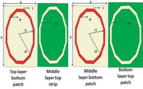
The proposed FSS is composed of one single sided patch layer, one strip layer and one double sided patch and strip layer. The shape of the design selects dodecagon which is a 12-segment polygon. The layers are arranged in such a manner, which are complement to each other. The proposed design also satisfies the condition ofP < (1+sinλ0 θ) whereλ0 is the wave length of the proposed design, andP is the
periodic unit cell dimension of the design [1]. The geometry of the proposed unit cell of three layered FSS is shown in Figure 1. The perspective view of single unit cell FSS design is shown in Figure 2.
Figure 1. Unit cell design of three layered FSS design.
The dimensions of the unit cell areP = 7.5 mm,r0(outer radius) = 3.4 mm (diameter of 6.8 mm),
r1(inner radius) = 3 mm (diameter of 6 mm), spacing between layers s = 0.7 mm, w = 0.4 mm,
Figure 2. Perspective view of multi-layer unit cell FSS design.
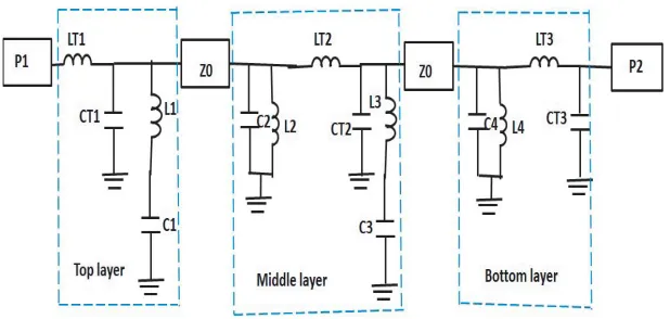
Figure 3. Equivalent circuit model of three layered FSS design.
3. EQUIVALENT CIRCUIT MODEL OF UNIT CELL FSS LAYER
An equivalent circuit model for the unit cell of the three layer FSS is shown in Figure 3. The series combination of inductor L1 and capacitor C1, L3 and C3 represents patch layers. The parallel combination of InductorL2 and capacitor C2,L4 andC4 represents strip layers. All the three layers of FSS are modeled as series and parallel LC resonators. The three layers are placed complement to each other which gives sharp band stop characteristics. The air gap between the FSS layers is represented as transmission lines as T L1 and T L2 with a free space characteristic impedance of Z0 of 377 Ω. The
values of LT1 =LT2 =LT3 and CT1 =CT2 =CT3 can be calculated from Telegrapher’s model [20] using TEM transmission line equations which are
LT1 = LT2 =LT3 =μ0μrT (1)
CT1 = CT2 =CT3 =ε0εrT (2)
In the above equations ‘T’ is the substrate thickness of 0.4 mm for all the three layers and
μ0(free space permeability) = 4π×10−7H/m, where ε0(free space permittivity) = 8.85×10⁻¹²F/m.
The equivalent circuit parameter values for inductance and capacitance are obtained by using equations [28],
L = μ0μeffP cosθ 2π ln
1
sinπw 2P
106 Shaik and Shambavi
C = 40εeffP cosθ 2π ln
1
sin πs 2P
(4)
where μ0(free space permeability) = 4π ×10−7H/m, μeff (effective permeability) = (μr+ 1)/2 = 1, ‘P’ is the unit cell dimension of the frequency selective surface, ‘w’ the width of the unit cell, and ‘s’ the spacing between the unit cell, whereas ε0(free space permittivity) = 8.85×10⁻¹²F/m,
εeff(effective permittivity) = (εr+ 1)/2 = 2.7. The above parameters require to estimate LC values. The top layer is the patch layer which acts as a band stop filter whose equivalent circuit is the combination of series Land C values, whereas the strip is the parallel combination ofLand C values. But there is height variation between the bottom and top layers. The same L and C values for both double side layers are applied. Due to height variations in between the layers obtaining similar notches is difficult due to inductance and capacitance effects. To get an output similar to simulated HFSS result, the potential ranges of the inductor and capacitance are obtained as 6.8 nH≤L= 9.8 nH and 0.023 pF ≤C ≤0.07 pF. The series inductors LT1, LT2, LT3 and shunt capacitors of CT1, CT2, CT3 are used for transmission line representation of substrate in the circuit. The characteristic impedance of the transmission line section of substrate is calculated usingZ0/√εr, whereεr is the relative permittivity
of the dielectric, andZ0 is free space wave impedance. Both ends of the FSS layers are modeled here
with a characteristic impedance of free space which is 377 Ω [20, 26].
The LC circuit parameters after being optimized using AWR software for different layers are
L1 = 3.6 nH, C1 = 0.06 pF, L2 = 7.7 nH, C2 = 0.06 pF, L3 = 7.7 nH, C3 = 0.06 pF, L4 = 7.7 nH,
C4 = 0.03 pF, and the values obtained using Eqs. (1) and (2) for transmission line are LT1 =LT2 =
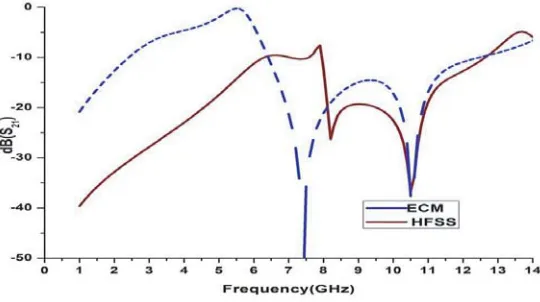
LT3 = 0.5 nH andCT1 =CT2 =CT3 = 15.5 fF and Zo= 377 Ω, respectively. The agreement between the above full wave simulation (HFSS) in Figure 4 and equivalent circuit model results is within the range and worthy for the three layered FSS design. There is height variation between the layers, considering that the height variation in the equivalent circuit model is difficult because there will be only slight variation in the bandwidth, transmission zero and transmission coefficient values obtained.
Figure 4. Comparision of simulated and ECM output.
4. RESULTS AND DISCUSSION
(a)
(b)
Figure 5. (a) TE polarization of FSS at oblique incidence angles. (b) TM polarization of FSS at oblique incidence angles.
the two polarizations for oblique angles of incidence up to 45◦. The various oblique angles of incidences of both TE and TM are shown in Figure 5(a) and Figure 5(b).
The simulation is also carried out for various other air spacing differences of 2.5 mm and 5 mm. The air gap separation of various heights comparison is shown in Figure 6. Better results obtained for
108 Shaik and Shambavi
Figure 6. Comparison of air gap separation between layers of FSS design.
Figure 7. Surface current distribution in the layers at center frequency range.
distribution observed near the bands of 8.2 GHz and 10.5 GHz is more. The compact thin three layer design is suitable for the reflection of the entire X band ranging from 8 to 12.5 GHz.
The comparisons of previous references and the proposed designs are presented in Table 1.
Table 1. Comparison with the previous multilayer FSS designs offered in the literature.
Parameter Ref. [20] Ref. [22] Proposed
Unit cell (mm) 11 mm×11 mm 5 mm×5 mm 7.5 mm×7.5 mm
Frequency band (GHz) 4–7 26–40 8–12.5
Layers 2 4 3
Spacing between layers 4 mm 2.5 mm 2 mm
Angular stability 60◦ 25◦ 45◦
Method Cascading Cascading cascading
Fractional Bandwidth 60% NA 45%
Dielectric substrate, thickness of substrate 4.4, 1.2 mm 2.2, 0.127 mm 4.4, 0.4 mm
5. EXPERIMENTAL VALIDATION
To verify the validity of the proposed design, a prototype with 30×30 unit cells array is fabricated. The dimensions of the dodecagon FSS array are 225×225 mm2. The fabricated designs of three layered dodecagon FSS patch array and strip array are shown in Figures 8(a) and 8(b). The prototype of the
(a) (b)
(c)
Figure 8. (a) Fabricated 30×30 cells patch array. (b) Fabricated 30×30 cells strip array. (c) Three layer 30×30 cells FSS array with air gap separation of 2 mm.
(a) (b)
110 Shaik and Shambavi
fabricated three layered FSS is shown in Figure 8(c).
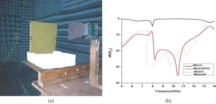
The measurement has been carried out in a microwave anechoic chamber using two horn antennas. Initially calibration has been done for S21 measurement without FSS array. After calibration the
dodecagon FSS array is placed between two horns antennas. The distance between the two horn antennas is 1.5 meters, and FSS is placed in middle of two horn antennas. The normal incidence wave is impinging on the FSS array using transmitting antenna and the receiving antenna reflecting the X band. The measurement setup and the comparison of measured and simulation results are shown in Figures 9(a) and 9(b). There is a small inconsistency in the measured output due to fabrication tolerances.
6. CONCLUSION
In this paper a low profile band stop dodecagon FSS array based on multilayer concept is designed, analyzed using equivalent circuit model, fabricated and measured for X band applications. The three layer wide band stop FSS in the frequency range from 8 GHz to 12.5 GHz is presented with center frequency of 10.25 GHz with air gap of 0.067λ0. The novelty of this design compared with the previous
FSS researches is the overall thickness of the design and miniaturized unit cell dimensions. This is not refined compared to previous designs, but it is suitable for miniaturized multi-layer frequency selective surface for X band applications. The equivalent circuit model of three layer FSS is presented in order to obtain equivalent LC parameters. The three layer FSS is insensitive to oblique angles of incidences up to 45◦ for both polarizations. At the same time the fractional bandwidth obtained is greater than 40% with respect to center frequency. Measured results and equivalent circuit results are confirmed with simulation results in this communication. It is suitable for the applications of X band reflection and for enhancing directivity and gain of compact antennas when being used as reflectors.
REFERENCES
1. Munk, B. A.,Frequency Selective Surfaces: Theory and Design, John Wiley & Sons, 2005. 2. Vardaxoglou, J. C.,Analysis and Design, Taunton, UK, 1997.
3. Azemi, S. N., K. Ghorbani, and W. S. T. Rowe, “3D frequency selective surfaces,” Progress In Electromagnetics Research C, Vol. 29, 191–203, 2012.
4. Kurra, L., M. P. Abegaonkar, A. Basu, and S. K. Koul, “FSS properties of a uniplanar EBG and its application in directivity enhancement of a microstrip antenna,”IEEE Antennas and Wireless Propagation Letters, Vol. 15, 1606–1609, 2016.
5. Smith, T., U. Gothelf, O. S. Kim, and O. Breinbjerg, “An FSS-backed 20/30 GHz circularly polarized reflectarray for a shared aperture L-and Ka-band satellite communication antenna,”IEEE Transactions on Antennas and Propagation, Vol. 62, No. 2, 661–668, 2014.
6. Akbari, M., H. A. Ghalyon, M. Farahani, A. R. Sebak, and T. A. Denidni, “Spatially decoupling of CP antennas based on FSS for 30-GHz MIMO systems,” IEEE Access, Vol. 5, 6527–6537, 2017. 7. Mias, C., “Frequency selective surfaces loaded with surface-mount reactive components,”
Electronics Letters, Vol. 39, No. 9, 724–726, 2003.
8. Batchelor, J. C., E. A. Parker, J. A. Miller, V. Sanchez-Romaguera, and S. G. Yeates, “Inkjet printing of frequency selective surfaces,” Electronics Letters, Vol. 45, No. 1, 7–8, 2009.
9. Whittow, W. G., Y. Li, R. Torah, K. Yang, S. Beeby, and J. Tudor, “Printed frequency selective surfaces on textiles,” Electronics Letters, Vol. 50, No. 13, 916–917, 2014.
10. Whittow, W. G., Y. Li, R. Torah, K. Yang, S. Beeby, and J. Tudor, “Printed frequency selective surfaces on textiles,” Electronics Letters, Vol. 50, No. 13, 916–917, 2014.
11. Chaharmir, M. R., J. Shaker, and H. Legay, “Dual-band Ka/X reflectarray with broadband loop elements,” IET Microwaves, Antennas& Propagation, Vol. 4, No. 2, 225–231, 2010.
13. Sivasamy, R., L. Murugasamy, M. Kanagasabai, E. F. Sundarsingh, and M. G. N. Alsath, “A low-profile paper substrate-based dual-band FSS for GSM shielding,” IEEE Transactions on Electromagnetic Compatibility, Vol. 58, No. 2, 611–614, 2016.
14. Werner, D. H. and D. Lee, “A design approach for dual-polarized multiband frequency selective surfaces using fractal elements,”IEEE Antennas and Propagation Society International Symposium, 2000, Vol. 3, 1692–1695, IEEE, Jul. 2000.
15. Li, D., Y. J. Xie, P. Wang, and R. Yang, “Applications of split-ring resonances on multi-band frequency selective surfaces,”Journal of Electromagnetic Waves and Applications, Vol. 21, No. 11, 1551–1563, 2007.
16. Rashid, A. K. and Z. Shen, “A novel band-reject frequency selective surface with pseudo-elliptic response,”IEEE Transactions on Antennas and Propagation, Vol. 58, No. 1, 1220–1226, 2010. 17. Azemi, S. N., K. Ghorbani, and W. S. Rowe, “A reconfigurable FSS using a spring resonator
element,” IEEE Antennas and Wireless Propagation Letters, Vol. 12, 781–784, 2013.
18. Majidzadeh, M., C. Ghobadi, and J. Nourinia, “Novel single layer reconfigurable frequency selective surface with UWB and multi-band modes of operation,” AEU — International Journal of Electronics and Communications, Vol. 70, No. 2, 151–161, 2016.
19. Encinar, J. A. and J. A. Zornoza, “Broadband design of three-layer printed reflectarrays,” IEEE Transactions on Antennas and Propagation, Vol. 51, No. 7, 1662–1664, 2003.
20. Chatterjee, A. and S. K. Parui, “A dual layer frequency selective surface reflector for wideband applications,” Radioengineering, Vol. 25, No. 1, 67–72, 2016.
21. Al-Joumayly, M. A. and N. Behdad, “A generalized method for synthesizing low-profile, band-pass frequency selective surfaces with non-resonant constituting elements,”IEEE Transactions on Antennas and Propagation, Vol. 58, No. 12, 4033–4041, 2010.
22. Martinez-Lopez, L., J. Rodriguez-Cuevas, J. I. Martinez-Lopez, and A. E. Martynyuk, “A multilayer circular polarizer based on bisected split-ring frequency selective surfaces,” IEEE Antennas and Wireless Propagation Letters, Vol. 13, 153–156, 2014.
23. Li, Y., L. Li, Y. Zhang, and C. Zhao, “Design and synthesis of multilayer frequency selective surface based on antenna-filter-antenna using Minkowski fractal structures,” IEEE Transactions on Antennas and Propagation, Vol. 63, No. 1, 133–141, 2015.
24. Chaharmir, M. R. and J. Shaker, “Design of a multilayer X-/Ka-band frequency-selective surface-backed reflectarray for satellite applications,” IEEE Transactions on Antennas and Propagation, Vol. 63, No. 1, 1255–1262, 2015.
25. Tao, K., B. Li, Y. Tang, and Q. Wu, “Multi-layer tri-band frequency selective surface using stepped-and uniform-impedance resonators,” Electronics Letters, Vol. 52, No. 8, 583–585, 2016.
26. Omar, A. A. and Z. Shen, “Thin bandstop frequency-selective structures based on loop resonator,”
IEEE Transactions on Microwave Theory and Techniques, Vol. 65, No. 7, 2298–2309, 2017. 27. Fallah, M. and M. Hashem Vadjed-Samiei, “Designing a bandpass frequency selective surface based
on an analytical approach using hexagonal patch-strip unit cell,” Electromagnetics, Vol. 35, No. 1, 25–39, 2015.