Abstract
BLUE, MICHAEL DEWAYNE. Development of a Non-Contacting Capacitive
Displacement Sensor for Integrated Chatter Prediction on High Speed Machining Centers.
(Under the guidance of Gregory Dale Buckner.)
Chatter is an unstable forced vibration of the cutting tool during machining processes that can limit the productivity of high-speed machining. Chatter increases tool and machine wear rates, reduces tolerances, degrades surface finish, and can result in tool breakage. For
these reasons, its avoidance is critical. Researchers at N.C. State University are focusing on the development of technologies to detect and avoid this dynamic instability. The
primary objective of this project is to develop accurate, high bandwidth, low cost capacitive displacement sensors for use with a prototype electromechanically actuated chatter
prediction device. These application-specific sensors are required to have at least 1.0 µm
resolution, 1.0 kHz bandwidth, and linearity over the desired measurement ranges. These
sensors must output analog DC voltages proportional to the vertical and horizontal displacements of a specifically engineered machine tool. A simulation-based design
Development of a Non-Contacting Capacitive
Displacement Sensor for Integrated Chatter Prediction
on High Speed Machining Centers.
by
Michael Dewayne Blue
A thesis submitted to the Graduate Faculty of North Carolina State University
in partial fulfillment of the requirements for the Degree of
Master of Science
Mechanical and Aerospace Engineering
Raleigh, North Carolina
May, 2003
APPROVED BY:
________________________________ _________________________________ Dr. G. Bilbro Dr. K. Peters
(Advisory Committee Member) (Advisory Committee Member)
Biography
Michael was born in Charlotte, North Carolina. Over time, he began to realize the impact that engineering has on our everyday lives and decided to lay the foundations for an
engineering-related career. After graduation from North Mecklenburg High School in June of 1998, he attended North Carolina State University where he received a bachelor’s degree in mechanical engineering in May 2002.
He selected the field of mechanical engineering due to the broad scope of engineering exposure that the degree entails. Michael also took an interest in business because he
realized its importance as related to accomplishing financial goals and engineering management. As undergraduate graduation grew closer and the economy began to
stammer, he decided to continue his educational endeavors with graduate study. His interest in electromechanical systems guided him to a thesis research project that was primarily electrical in nature and involves non-contacting actuation and measurement for
Acknowledgements
I have tremendously enjoyed working on this project, which would not have been possible without the help of many generous people.
I will always have gratitude for the assistance, encouragement, and guidance that Mr. Larry K. Baxter has provided throughout this project.
I deeply appreciate and will forever be thankful for all of the encouragement, support, values, and enjoyment my parents have given me.
I would also like to thank the members of this research project, Don Caulfield and Aaron Kiefer, and the sponsor, VulcanCraft LLC and Dr. Donald M. Esterling, for their
teamwork and support.
Financial support provided by the North Carolina Space Grant Consortium was greatly appreciated.
Others who have my appreciation for their assistance include Heeju Choi, Mike Breedlove, Robert Hughes, Rudy Salas, and Skip Richardson.
Table of Contents
List of Tables………vi
List of Figures………..vii
1. Introduction 1 2. Background 5 2.1 High Speed Machining (HSM)... 5
2.2 Chatter ... 7
2.3.1 Regenerative Chatter ... 8
2.3.2 Stability Lobe Diagrams (SLDs)... 10
2.3 Predicting, Identifying, and Controlling Chatter ... 13
3. Capacitive Sensing 15 3.1 Overview ... 15
3.2 Electrostatics, Electrodynamics, & Capacitance ... 15
3.3 Displacement Sensing ... 19
3.3.1 Non-contact Sensing Technologies... 19
3.4 Sensor Terminology ... 22
3.4.1 Linearity... 22
3.4.2 Sensitivity ... 23
3.4.3 Resolution ... 23
3.4.4 Accuracy ... 24
3.4.5 Precision ... 24
3.5 Capacitive Sensor Design Specifications... 24
4. CDS Electrical Design 28 4.1 Capacitive Sensing Circuits... 28
4.2 Synchronous Demodulation Circuit... 31
4.2.1 Excitation and Demodulator Control ... 33
4.2.2 Sensing and Guarding... 34
4.2.3 Demodulation and Filtering ... 36
4.3 Component Selection ... 37
4.3.1 AD823 FET Operational Amplifier ... 38
4.3.2 TLC555 Timer... 41
4.3.3 MAX4053 Multiplexer... 42
4.3.4 74HC74 Flip-Flop ... 43
4.3.5 Other Components & Cost... 43
5. CDS Circuit Analysis 45 5.1 Overview ... 45
5.2 Circuit Modeling... 45
5.2.1 Sensing Circuitry ... 46
5.4 Noise Sources & Their Impact... 58
5.5 Sources of Nonlinearity... 61
6. CDS Mechanical Design 62 6.1 Design Overview... 62
6.2 Design Specifications... 63
6.2.1 Materials & Connectors ... 64
6.2.2 Probe Geometry ... 65
6.2.3 Probe Guards... 67
6.2.4 Probe Analysis ... 68
6.2.5 Probe Support, Positioning, and Other Considerations... 70
6.2.6 Printed Circuit Board (PCB) & Enclosure... 72
7. Experimental Evaluations 78 7.1 Test Objectives ... 78
7.2 Static Measurements ... 78
7.3 Dynamic Testing ... 94
7.3.1 Voice coil-Actuated Test Rig... 94
7.3.2 Haas VF-1 5-axis Vertical Milling Center... 99
7.4 Summary of Test Results ... 103
8. Conclusions and Future Work 105 8.1 Conclusions... 105
8.2 Improvements & Future Work ... 106
9. References 107
Appendix A: Parts List 110 Appendix B: CAD Drawings 111
List of Tables
Table 3.1: Summary of CDS Design Specifications...27
Table 5.1: Circuit modeling assumptions ...46
Table 5.2: Steady-state simulation input values: static ...55
List of Figures
Figure 2.1: F-15 speed brake produced by Boeing, St. Louis, MO ...6
Figure 2.2: In-phase cut [41]...8
Figure 2.3: Out-of-phase cut [41] ...9
Figure 2.4: Rough surface finish caused by tool chatter [8] ...10
Figure 2.5: Stability lobe diagram [41]...11
Figure 3.1: Electric field lines for (a) a positive point charge, (b) two point charges of equal polarity, and (c) two point charges of opposite polarity [25]...16
Figure 3.2: Charged parallel plates with lines of electric flux [3] ...16
Figure 3.3: (a) charge accumulation on plates [25] and (b) dielectric polar charges and dipole moments between charged parallel plates [24]...18
Figure 3.4: Capacitive probe with sub-nanometer resolution [30]...22
Figure 3.5: Average compliance for Haas VF1 5-axis vertical spindle milling center...25
Figure 4.1: DC sensor circuit schematic...29
Figure 4.2: Oscillator-based circuit schematic...30
Figure 4.3: AC, bridged demodulation circuit schematic (C2 variable, C1 reference) ...31
Figure 4.4: AC, single-ended demodulation circuit schematic ...31
Figure 4.5: Complete CDS circuit schematic with labeled subcircuitry...32
Figure 4.6: CDS circuit functional overview...33
Figure 4.7: Excitation and demodulator control circuitry...34
Figure 4.8: (a) Sensing and guarding circuitry (b) Sensing and guarding functional representation 35 Figure 4.9: (a) Synchronous demodulator circuitry (b) Demodulation illustration occurring at S3 ..37
Figure 4.10: Timer operation diagram ...42
Figure 4.11: Multiplexer operation diagram...42
Figure 5.1: Sensing circuitry schematic...46
Figure 5.2: Linear charging/discharging of Cs...49
Figure 5.3: Nonlinear charging/discharging of Cs(red)...50
Figure 5.4: Adjustment of VR1 to correct charging nonlinearity and gain reduction ...51
Figure 5.5: Demodulation Circuit Schematic...52
Figure 5.6: PSPICE CDS circuit schematic ...54
Figure 5.7: PSPICE simulation results: Static voltage output vs. displacement...55
Figure 5.8: PSPICE simulation results: Static voltage output vs. displacement with added guard capacitance ...56
Figure 5.9: PSPICE simulation results: transient response of amplifier A1 output voltage...57
Figure 5.10: PSPICE simulation results: zoomed transient response of amplifier A1 output voltage ...58
Figure 6.1: Complete CDS sensor system hardware ...62
Figure 6.2: CDS measurement setup ...63
Figure 6.3: Probe materials aluminum and UHMW polyethylene ...65
Figure 6.4: SMA probe connector...65
Figure 6.5: (a) Specially designed tack-tool with holder (b) x-axis measurement probe ...66
Figure 6.6: z-axis measurement probe...67
Figure 6.7: Parallel plate configuration with guard (left) and without a guard (right) ...68
Figure 6.8: Probe stand...71
Figure 6.9: Frequency response results from modal hammer tests ...72
Figure 6.10: Entire circuit photo...73
Figure 6.11: Circuit isolation scheme ...73
Figure 6.12: Bottom later (left) and top layer (right) of PCB...74
Figure 7.4: Consolidated data from the capacitive (left) and optical experimental data (right). ...81
Figure 7.5: Manufacturer-provided the RC25 ODS calibration curve...82
Figure 7.6: ODS measured micron versus HAAS theoretical position to show minimal hysteresis and/or backlash...83
Figure 7.7: Horizontal static tests: CDS voltage output vs. ODS displacement (left) and CDS voltage variance vs. average ODS displacement (right) ...84
Figure 7.8: Horizontal static test: Average CDS output voltage vs. ODS displacement measurements ...84
Figure 7.9: Horizontal static test: horizontal CDS vs. ODS displacement measurements...85
Figure 7.10: Horizontal static test: Average CDS vs. ODS displacement measurements ...86
Figure 7.11: Full scale error (left) and of ODS reading error (right). ...86
Figure 7.12: Horizontal static test with second data set: CDS displacement vs. ODS displacement .87 Figure 7.13: Horizontal static test with second data set: Full scale error...88
Figure 7.14: Minimization of vertical surface deviations...89
Figure 7.15: Vertical static test: Consolidated data from the capacitive (left) and optical experimental data (right). ...90
Figure 7.16: Vertical static test: CDS voltage output vs. ODS displacement duel variance point array...91
Figure 7.17: Vertical static test: Average CDS output voltage vs. ODS displacement measurements ...91
Figure 7.18: Vertical static test: Average CDS output voltage vs. ODS displacement measurements ...Error! Bookmark not defined. Figure 7.19: Voicecoil-actuated dynamic testing setup ...95
Figure 7.20: Dynamic test of CDS vs. ODS constant gap noise levels: a) time responses b) frequency responses (CDS blue, ODS red) ...96
Figure 7.21: Dynamic test of CDS vs. ODS at 125 Hz: a) time response b) zoomed time response (CDS blue, ODS red) ...97
Figure 7.22: Dynamic test of CDS vs. ODS at 125 Hz: a) frequency response b) zoomed frequency response (CDS blue, ODS red)...97
Figure 7.23: Hammer impact testing on voicecoil-actuated experimental setup ...98
Figure 7.24: Dynamic test of CDS bandwidth over 900 Hz (CDS blue, ODS red)...99
Figure 7.25: Dynamic verification with z-direction forcing and z-axis measurement - (a) time responses (b) frequency responses (CDS blue, ODS red) ...101
Figure 7.26: Dynamic verification with z-direction forcing and x-axis measurement - (a) time responses (b) frequency responses (CDS blue, ODS red) ...102
Figure 7.27: Dynamic verification with x-direction forcing and z-axis measurement - (a) time responses (b) frequency responses (CDS blue, ODS red) ...103
1. Introduction
Recent advancements in the design of machining centers have increased commercially
available spindle speeds to over 40,000 rpm. Enhanced machine capabilities have given rise to the practical implementation of high speed machining (HSM). While HSM is
difficult to define precisely, it generally involves running machines at higher spindle speeds and higher feed rates, thereby increasing production rates in manufacturing shops. HSM is gaining widespread acceptance in manufacturing sectors, with its adoption being
led by the aerospace industry. Large aluminum parts can be produced from a single workpiece using HSM methods, instead of requiring assembly from many components.
Besides the time saved in assembly, other benefits include reduced lead time, reduced waste, and parts that are simultaneously lighter, stronger, and cheaper. The tool and die industry is also rapidly adopting HSM [24]. The use of HSM will become more
widespread in industry as its benefits become better understood.
There are problems associated with the increased spindle speeds of HSM, most notably tool chatter. Chatter is an unstable vibration of the cutting tool [9] that is a function of both spindle speed and cutting depth. It can cause problems ranging from poor surface
finish to machine damage and personal injury. The intuitive method of chatter avoidance dictates that whenever chatter is encountered the spindle speed should be reduced. This
Several methods have been devised to control, prevent, or avoid chatter. These methods range from sampling acoustic signals while cutting is in progress [1] to predicting machine behavior by a priori characterization of the system dynamics [[2],[10]]. Chatter
control methods that use real-time measurements can be effective in controlling chatter after its onset, but these techniques have the disadvantage of not being able to prevent
chatter from occurring.
Predictive methods offer the benefit of avoiding the onset of chatter in the first place.
Sophisticated techniques such as finite element analysis (FEA) can be used to characterize the machine’s dynamics. FEA can accurately predict the frequency response
characteristics of the system [10], but requires experimental verification and the input of experimentally derived parameters. It is also time consuming and computationally intensive. Experimental modal testing provides the essential information of FEA, namely
the system’s frequency response functions (FRFs), and is quicker to perform. Unfortunately, modal testing requires specialized equipment and skills that make it impractical for widespread industrial adoption.
Researchers at NIST have devised an automated technique that can produce frequency
response information quickly without requiring special skills [9]. This method uses a stationary permanent magnet to impart excitation forces to a rotating tool. Tool displacement is measured using optical sensors, and frequency response information is
off-the-shelf sensors and data acquisition hardware and software) suggest that a system using this method would be inexpensive to produce. However, the inability to control the applied force magnitudes using a permanent magnet restricts the feasibility of this
approach.
The primary goal of this research is to develop capacitive displacement sensors for use with a refined, automated system that measures the frequency response characteristics of high-speed milling machines and predicts stable operating regions. This automated
system provides the benefits of the NIST scheme (ease of use, minimal testing time, low expenses of production), but overcomes the limitations of passive excitation by
introducing a controlled, non-contacting electromechanical actuator. For accurate frequency response characteristics to be obtained, non-contacting measurement is crucial. The capacitive displacement sensors outlined in this thesis enable accurate prediction of
the frequency response characteristics without sacrificing device functionality or cost. Two prototype capacitive displacement sensors (CDSs) are designed, fabricated, and experimentally validated by direct comparison with a commercial optical displacement
sensor (ODS) on a CNC machining center.
Preliminary results show that the capacitive displacement sensor has sufficient bandwidth, sensitivity, resolution, and accuracy to be an effective component in an automated chatter prediction system. The capacitive displacement sensors are
2. Background [28]
2.1 High Speed Machining (HSM)
HSM is currently finding application mainly in the aerospace industry, although a recent white paper from Unigraphics, Inc. suggests that “approximately 30 percent of the
companies in the U.S. and Japan are already using HSM, with the number even greater in Germany at 40 percent. The remaining companies in all these countries are considering making an investment in HSM or are interested in this new technology” [41]. HSM will
find its way into smaller machine shops as it becomes better understood and its drawbacks are addressed.
The main advantage of HSM is that it gives manufacturers a practical and cost-effective way to produce parts that cannot be as easily produced using standard machining
processes. Examples of this benefit can be found in aircraft parts produced by Boeing at their Advanced Materials Fabrication Facility in St. Louis, MO. These parts are
simultaneously lighter, stronger, cheaper, and require a small fraction of the machine time previously needed [24]. One of the parts Boeing produces using HSM is the F-15 fighter’s speed brake (Figure 2.1). This part was previously assembled from 500
individual components, but HSM enables Boeing to mill this part out of a single block of aluminum. The manufacturing lead time for this part has reduced from three months to
Figure 2.1: F-15 speed brake produced by Boeing, St. Louis, MO
The absence of stress concentrations associated with fastener holes is an added benefit of
parts machined out of a single block instead of assembled from many parts. Residual stresses resulting from imprecise assembly are also eliminated. The part’s strength and reliability can therefore be increased using HSM techniques.
Another example of Boeing’s success using HSM and a good illustration of its
advantages is the F/A-18E/F tactical fighter. As a result of implementing HSM, this version of the F-18 fighter is 25% larger than previous versions yet uses 42% fewer parts [24].
The benefits of HSM include:
drastically reduced lead time •
• • • • • •
increased production speeds fewer parts to track
reduced number of suppliers higher strength
This process is more than simply running a machine wide open to crank out parts. There are problems and hardware limitations associated with higher spindle speeds. An important limitation to high speed, high feed machining is forced vibrations.
Uncontrolled vibrations of the cutting tool, called chatter, can produce unacceptable surface finishes on parts and can result in broken cutting tools.
2.2 Chatter
Chatter is an unstable forced vibration of the cutting tool during a machining process.
Problems caused by chatter include:
• tool breakage and possible personal injury or machine damage • accelerated tool and machine wear rates
• reduced tolerances on machined parts
• poor surface finish requiring excessive hand-finishing • increased scrap (from unacceptable products)
• excessive machining noise
• problems machining thin-walled parts
Chatter in milling is caused by the self-excitation of the machine tool. The two main sources of self-excitation in machining as defined by Tlusty [39] are mode coupling and
‘regeneration of waviness’. Mode coupling is a two-dimensional phenomenon that occurs when the tool experiences force feedback in at least two directions simultaneously. Vibrations in these two directions are of the same frequency and have a
mechanism in milling and is the focus of this thesis. A third cause of chatter is impact dynamics, which occurs at low spindle speeds. Since one chief aim of HSM is to maximize machine spindle speed, this mechanism was not considered.
2.3.1 Regenerative Chatter
Regenerative chatter is caused by surface variations associated with previous cuts. As
each tool flute passes over the surface of the material and makes a cut, it creates an undulating surface. As the next flute passes and makes a cut, it encounters this wavy surface. If the vibrations of this flute are in phase with the wave left by the previous flute
cut, the depth of cut remains constant and the chip produced has a constant thickness. A diagram of this ‘in-phase cut’ is shown in Figure 2.2.
Cutting
tool Previouscut waves Current cut
Figure 2.2: In-phase cut [39]
During ‘in-phase’ cutting, the cutting force amplitude remains essentially constant and
chatter is less likely to occur. If the next flute that passes over the wavy surface vibrates
‘out-of-phase’ with the surface waves, the thickness of the chip produced is not constant.
Cutting
tool Previouscut waves Current cut
Figure 2.3: Out-of-phase cut [39]
In this case, the varying chip thickness creates a varying force on the cutting tool. This
harmonic variation in cutting force can result in resonant vibration of the milling tool, or regenerative chatter.
Depth of cut has a significant effect on the vibrational stability of the cutting tool and hence on regenerative chatter. When the cut is shallow, the cutting force amplitudes are
small, and cutting is stable at all spindle speeds. The maximum cutting depth that results in stable machining at all spindle speeds is called the limit of stability, denoted blim. As
will be noted in the next section, certain spindle speeds allow stable cuts at deeper cutting depths. To maximize production, it is desirable to make the deepest cuts possible at the highest spindle speeds possible. These operating conditions will cause chatter unless the
previously discussed in-phase tool cuts can be made or the vibrations are controlled and prevented from growing. If machining can be performed in a way that creates in-phase
When a cutting tool chatters, the magnitude of vibration causes the tool to lose contact with the workpiece. This loss of contact results in a rough surface finish. This rough finish can require extra hand finishing of the part, or it can exceed tolerances and
requiring scrapping of the part. An extreme example of this rough surface effect is shown in Figure 2.4.
Figure 2.4: Rough surface finish caused by tool chatter [18]
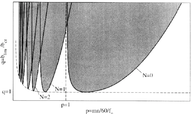
2.3.2 Stability Lobe Diagrams (SLDs)
Cutting with in-phase tool vibrations can be accomplished by cutting with a flute passing frequency at or near integer divisions of the natural frequency of the cutting
tool/spindle/machine system [9]. The flute passing frequency, ff, is the tool speed multiplied by the number of flutes. For example, if the spindle speed of a 2-flute tool is 15,000 rpm the flute passing frequency is:
(
flutes)
Hz rpmff 2 500
min sec 60
000 , 15
=
Regions of cutting stability lie near these flute passing frequencies. The importance of these stable cutting regions is that cutting depth can be significantly increased [10]. This increase in achievable cutting depth is depicted graphically on a Stability Lobe Diagram
(SLD), a plot of stable cutting depth vs. spindle speed. A representative SLD is shown in Figure 2.5.
Figure 2.5: Stability lobe diagram [39]
The limits of stable cutting depth are delineated with solid lines. Cutting depths above these lines (in the shaded areas) are unstable, while cutting depths below these limits
(unshaded regions) are stable. The flat dashed line represents the stability200
limit cutting depth blim, which is the maximum depth a stable cut can be made at all spindle speeds. Analytical derivations of SLDs were developed in the 1960’s by Merritt
The frequency response function (FRF) of the tool/spindle/machine system must be accurately known in order to create a SLD. The real component of this FRF generates
the stability lobes for regenerative chatter [33]:
(
FRF)
K b d s Re 2 1 µ −
= (2.2)
where:
b = stability lobe boundary (mm)
Ks = specific force of the workpiece material (N/mm2)
µd = directional orientation factor
Re(FRF) = real part of the tool/spindle/machine system FRF
The FRF also provides an estimate of the stability limit, blim for regenerative chatter [1]:
(
)
min s lim FRF Re K 2 1b = − (2.3)
The SLD in Figure 2.5 supports the intuitive reasoning that chatter can be eliminated by
decreasing the spindle speed, cutting depth, and feed rate [12]. At very low spindle speeds and feed rates the blim limit trends higher, indicating that deep stable cuts can be
made at these speeds. This increase in cutting stability at low spindle speeds is the results of process damping [39]. However, the SLD also shows that chatter can be eliminated by increasing the spindle speed to the next higher stability region. Working in these stability
reduced hand-finishing requirements. Since chatter is eliminated, damage to workpiece, tool, and milling machine is eliminated as well. Higher productivity is also a result, since the MRR has not been reduced to avoid chatter. Therefore, accurate prediction of
stability regions is a crucial enabling technology for HSM.
2.3 Predicting, Identifying, and Controlling Chatter
Chatter prediction generally involves analysis of system dynamics through mathematical relationships to generate a frequency response function, often through the use of finite
element analysis (FEA) programs. FEA can be used to predict the systems frequency behavior but not without the disadvantage of requiring validation with experimental
testing. To gain acceptance in industry, an automated process such as one developed by researchers at NIST that determines frequency response without any required skills from the end user is needed [9]. The idea behind this system is promising but involves a
permanent magnet as its actuation source, making it unable to control applied force magnitudes at any particular frequency.
The use of an electromagnetic actuator (EMA) allows for controllable force magnitudes and, when combined with receptance coupling analysis (RCSA), provides an automated
method of predicting stable cutting regions [18]. The basic idea behind the analysis is that the tool holder, spindle, and CNC machine have one frequency receptance while the tool itself has another. Initially, the entire system’s points of instability are analyzed with
ordinary machine cutting tools. The stable cutting regions are then realized for a variety of machine tools on the milling center.
An essential part of RCSA requires that the actuation and sensing methods do not interfere with the modal characteristics of the system and thus are non-contact. The
EMA provides effective non-contacting and controllable force input at a reasonable price. However, non-contact sensing poses a significant problem due primarily to associated costs. Thus, a fully functional, low cost, application-specific non-contacting
3. Capacitive Sensing
The reliable prediction of stable cutting regions for HSM applications requires accurate,
high-bandwidth displacement measurements to generate frequency response functions. Capacitive sensing can be used for such modal testing, provided the sensor is
appropriately designed. This section introduces the concept of capacitive sensing from an atomic level, briefly discusses displacement-sensing applications, reviews common sensor terminology, and presents design requirements for this application.
3.1 Overview
Capacitive sensing, as it relates to this application, involves monitoring the electromechanical changes in a variable-gap capacitor to infer distance measurements. The theory behind capacitive sensing relies heavily on Maxwell’s equations, particularly
the principles of electrostatics. The following sections provide a brief overview of electric field behavior and the constitutive relations that define the fundamentals of
capacitors.
3.2 Electrostatics, Electrodynamics, & Capacitance
Isolated point charges in free space (vacuum) can be visualized using electric field lines. The direction of a field line indicates the direction of an electrostatic force that would be
field lines for a positive point charge, two equally positive point charges, and two point charges of opposing polarity, respectively.
.
c
a b
Figure 3.1: Electric field lines for (a) a positive point charge, (b) two point charges of equal polarity, and (c) two point charges of opposite polarity [25]
The electric field lines in these figures demonstrate the tendency of like charges to repel and opposite ones to attract. These electric fields lines also represent associated attractive
or repulsive forces. However, the magnitudes of forces between charges, which can be calculated using Coulomb’s Law, are negligible for most capacitive sensor applications [20].
An electric field is created when two conductive parallel plates are charged with opposite
Displaced charges in electrostatic fields possess potential energy that is used to define voltage (V ), the potential energy per unit charge. Because electrostatic fields are
conservative, voltage equals the work required to move a test charge from a point of zero potential, often referred to as ground, to a point where the potential is measured. The
relation between the total charge (Q) accumulated on the plates and the potential energy
required to hold that charge is defined to capacitance (C), where
CV
Q= ( 3.1)
For the parallel plate configuration of Figure 3.2, the capacitance measured in
(
Coulombs Volt)
Farads is:
d A
C =εoεr ( 3.2)
where:
o
ε = dielectric constant (permittivity) of a vacuum, 8.8541878 ⋅10-12 F m
A = area in square meters
r
ε = relative permittivity of the medium with respect to a vacuum
d = distance between the plates in meters
causes a decrease in the local flux density and thus reduction in capacitance. There are techniques to reduce this inherent error in Equation 1.2, and they will be discussed during probe design (Section 6.2.3).
Current flow in a capacitive sensor can also be described at the atomic level, as shown in
Figure 3.3. Free electrons in the atoms of conductors drift in a direction opposite to the applied field, leaving a net positive charge in the direction of current. When two conductors are placed near each other but are separated by a non-conducting medium (a
dielectric material, as shown in
Figure 3.3), the medium determines the characteristics of current flow.
a b
Figure 3.3: (a) charge accumulation on plates [1] and (b) dielectric polar charges and dipole moments between charged parallel plates [13]
Displacement currents in dielectrics result from the reorientation of polar molecules. In highly resistive dielectric materials, the majority of current flows as the charges rush onto
current flows just long enough for the plates to reach equilibrium but then ceases. An alternating current (AC) source, however, the plates continually charge and discharge as long as the frequency of oscillation is shorter than the time required for the onset of
equilibrium.
3.3 Displacement Sensing
A vast array of sensor technologies exist for displacement measurement but not all are suitable for use in this HSM application. An introduction to non-contact sensing as it
applies to this application is presented, followed by a brief overview of capacitive displacement sensor technology.
3.3.1 Non-contact Sensing Technologies
There are numerous advantages of non-contact displacement measurement over
traditional methods, and these advantages have led to an increasing number of industrial applications. Though it is clearly evident, the most important advantage of non-contact sensing, as it relates to this application, is that it does not interfere with the mechanical
process being measured. Other attributes of non-contact sensing include the elimination of wear and damage to measured surfaces, improved reliability, and less required
maintenance. Primarily due to these advantages, there has been an increasing market trend toward non-contact sensors in the aerospace, medical, industrial, and automotive markets [8]. For example, the measurement of semiconductor substrates was drastically
by mechanical probes and eliminating contamination while maintaining high accuracy [37].
The appropriate sensor technology for this application was determined through design specifications such as cost, size, achievable resolution, and susceptibility to magnetic
field interference. LASER sensing technology generally cannot achieve sub-micrometer resolution, requires expensive machining, and exceeds the space limitations for the given application [34]. Inductive sensors, which utilize eddy currents induced on nearby
conductive targets, are influenced by nearby magnetic fields and are thus not suitable options for this application [35]. Ultrasonic sensors (often used for SONAR) are not
suitable for this application as they cannot detect such small displacement variations [36]. Generally, these non-contact sensors cannot achieve the resolution requirements of this application. Fiber optic displacement sensors, which use the emission and reception of
light to determine distance measurements, can easily meet the required resolution specifications [28] but are susceptible to variations in surface finish and are relatively expensive.
After eliminating most types of non-contact sensing techniques due to the
aforementioned limitations, a commercial capacitive sensor from a well-known manufacturer was tested to further validate that its suitability for this application. Bob Benjamin of Lion Precision [4] provided the capacitive sensor system with a universal
were comparable to those of the ODS and were validated through a series of EMA sweep tests.
Capacitive sensing offers several advantages that make it ideally suited to this application. The costs and required machining are not prohibitive. Sensors based on
capacitance technology meet the space requirements and are able to resist magnetically induced errors. Furthermore, capacitive sensing offers nearly unsurpassed accuracy in displacement sensing, design simplicity, immunity to light and sound, compensation for
environmental conditions, and probe shapes that can be refined to focus the sensing field on defined areas [7]. Also, these sensors can be built from a wide range of AC and DC
circuit topologies, depending on the application and design specifications.
Capacitive measurement applications include gap thickness, pressure, liquid level, and
flow rates. Figure 3.4 shows a capacitive displacement sensor from Polytech PI® that is capable of measurements down to 0.01 nm (10-12m), which is the highest commercially available resolution [29]. These sensors have a 3.0 kHz bandwidth, excellent long-term
Figure 3.4: Capacitive probe with sub-nanometer resolution [29]
3.4 Sensor Terminology
Capacitive sensing uses the constitutive relationships of capacitors (Equations 3.1 and
3.2) to infer displacement measurements that would be difficult or impossible to measure by other means. Capacitive sensors output a measurable electric quantity, typically a
voltage that is directly related to the state of a physical parameter, such as area or displacement. The sensor’s measured input-output relationship is called the calibration curve. Various characteristics related to the calibration curve quantify the performance
of the sensor, as defined below.
3.4.1 Linearity
It is desirable to have a perfectly linear relationship between the measured electrical output and the sensed physical parameter, but linear calibration curves are never
linear curve fit can be used to calculate linearity error [31]. This error can be expressed as a percentage of the sensor’s entire output range ‘% of F.S. (full scale)’ or as a percentage of the reading ‘% of R (reading).’
3.4.2 Sensitivity
The sensitivity is the change in output voltage that results from a change in the gap between target and sensor probe. The slope of the calibration curve, which plots the output voltage versus gap displacement, is essentially the sensor’s sensitivity over its
entire measurable range. This slope may change throughout the measurement range, though a high and constant sensitivity is always desired.
3.4.3 Resolution
The smallest change in gap that can be reliably measured is the sensor’s resolution. A
sensor’s resolution must be better than the required measurement accuracy. Often, the resolution of a sensor system is determined by electrical noise. Even for a constant gap, there are tiny, impulsive fluctuations in voltage that appear at the sensor output.
Resolution is then quantified by multiplying the sensitivity by these tiny fluctuations or noise floor. Also, because this low-level noise is spread through the entire frequency
3.4.4 Accuracy
Sensors are often characterized by their ability to provide an output that reveals the true value of the measured quantity. However, it is impossible to measure a true or perfect
quantity so a reference measurement is often made with a device of much higher resolution. The deviations from the reference value are then used to calculate error.
3.4.5 Precision
The capability of a measuring instrument to provide the same reading when repetitively
measuring the same quantity under the same conditions is referred to as precision. Precision implies an agreement between successive readings and a high number of
significant figures in the result. In a dartboard analogy, a precise player’s dart may hit the board repetitively in the same spot but an accurate and precise one would hit the bull’s-eye on each throw.
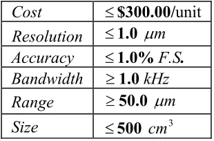
3.5 Capacitive Sensor Design Specifications
The most critical design requirement for this application, the sensor’s measurement
resolution, was determined from the electromechanical force capability of the actuator and the compliance of the tool/spindle system. As shown in Figure 3.5, the compliance
y = 0.0436x + 275.82 272.000 276.000 280.000 284.000 288.000
0.000 50.000 100.000 150.000 200.000
Applied Load (N)
To ol D efle ct io n (m ic ro ns )
Figure 3.5: Average compliance for Haas VF1 5-axis vertical spindle milling center
The tool displacement associated with an EM force of 30 N (<15% of the peak EM force)
is: m m N m N Compliance Force
d spindle 30 43.6 10 9 1.31 10 6 1.31µ
min
min = ∗ = ∗ ⋅ = ⋅ =
−
− ( 3.3)
Thus, a conservative sensor resolution of 1.0 um was selected as the design requirement.
The second most significant design requirement was sensor cost. Commercial sensors capable of 1.0 um resolution typically range in cost from $650 to $3000+ depending on type, quantity discounts, and included hardware. The second-generation EM chatter
prediction system, hereafter labeled VulcanCraft Performance®, utilizes EM actuation and non-contacting measurement to accurately determine a machine tool’s modal
be minimized. Multiple sensors may be required for this application, thus the final cost per sensor should be less than $300.
The required linear sensing range was determined by considering the maximum expected
tool deflection at resonance, dres, which increases by an order of magnitude:
m m
N N
Compliance Force
dres res 30 436 10 9 13.1µ
min ∗ = ∗ ⋅ =
= −
( 3.4)
The required sensor sensitivity, bandwidth, and accuracy were determined based on the
existing specifications of the existing EM chatter prediction system. The
9.1mV µmsensitivity of the ODS met all the needs of the existing system, and was set as
the benchmark for the CDS. Although the ODS has a sensor bandwidth of 20.0 kHz, 1.0
kHz was deemed appropriate based on typical modal characteristics of high-speed milling
spindles and tools (the first natural frequency of a 6” machine tool mounted in the spindle of a HAAS VF-1 5-axis milling machine is approximately 400 Hz). The requirement of
at least 1.0 % accuracy over the required measurement range of 30µm during operation
was determined to provide adequate prediction of modal characteristics using the receptance coupling technique [11].
Table 3.1: Summary of CDS Design Specifications Cost ≤$300.00/unit
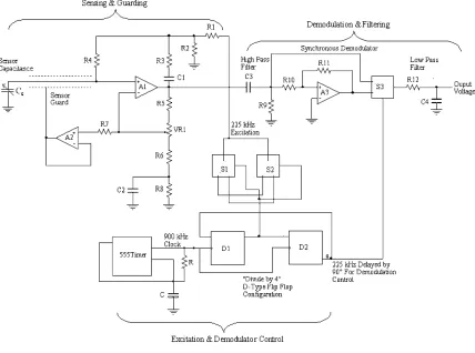
4. CDS Electrical Design
A primary objective of this research was to design a CDS circuit that met the functional specifications of an automated chatter prediction system for HSM applications. Various capacitive sensing circuits were evaluated, and a synchronous demodulation circuit was
selected. Characteristics and advantages of this circuit topology are presented through direct comparisons with alternative capacitive sensing circuits. Subsequently, factors that
influence circuit component selection are presented and described. This section concludes with an explanation of circuit operation with the selected components.
4.1 Capacitive Sensing Circuits
The simplest capacitive sensing circuit, Figure 4.1, applies a DC voltage to the sensing
plate of a variable gap capacitor. The other plate is ground-referenced through resistor R,
forming a high-pass filter. The amplified output voltage (V ) varies directly with gap
displacement at frequencies above
out
RC
12 −
1 , where R is the circuit resistance and C is the
sensor capacitance. Not only does this circuit suffer from low frequency data loss, it also provides no noise or interference filtering and may require specialized, ultra-high
impedance amplifiers [20]. A similar low-pass DC circuit can be realized by interchanging the R and C components of Figure 4.1. Although this may improve the
sensor’s low-frequency performance, an extremely large resistance would be needed to
achieve reasonable cutoff frequencies (on the order of 10 Ohms considering that the
capacitance C is on the order of 10 Farads). Because such large resistances would approach or exceed the input resistance of the op-amp, such a circuit is not practical for
this application. For these reasons, oscillator circuits are more commonly used for capacitive sensing applications requiring higher accuracy without low frequency losses.
Figure 4.1: DC sensor circuit schematic
The resonant frequencies of RC and LC circuits depend directly on capacitance, hence many types of oscillator and phase detection circuits exist for use with capacitive sensing
topologies. Figure 4.2 shows one example in which capacitance controls the frequency
output of a 555-type timer according to11.38RC. As the capacitance changes, the duty
cycle of the wave varies (see section 4.3.2 for timer description). A frequency counter or
time interval device then outputs a voltage based on accumulated pulses or time, respectively. This oscillatory circuit does not suffer from low frequency loss and is much
Though DC and oscillator circuits may be candidates for low or moderate accuracy requirements, respectively, the “most flexible and accurate method of measuring capacitance is to first apply a high frequency signal . . . through a known impedance to
the capacitor under test, then amplify the signal and apply it to a synchronous demodulator” [20]. This circuit topology, unlike DC and oscillator designs, does not require special high impedance amplifiers and can easily include shielding, guarding, and
filtering for noise reduction. Synchronous demodulator circuits are less sensitive to stray capacitance and can be built in either single-ended or bridge type configurations.
A typical AC bridge-type synchronous demodulation circuit topology is presented in Figure 4.3. In this circuit, an AC signal excites the variable-gap capacitor (C1 or C2)
under test while a multiplexer is used to demodulate its output before being converted to DC with a low-pass filter. Although AC bridge configurations have extremely high
sensitivity, they require precise calibration of a reference capacitor, are nonlinear with respect to the capacitive sensing element [26], generally have more circuit components, and thus are not ideal for low cost applications.
The single-ended synchronous demodulation circuit shown in Figure 4.6 also has high sensitivity, but with less components and complexity as compared to the AC bridge circuit. For this reason, it represents the ideal capacitive sensing circuit when
application-specific requirements (resolution, cost, maintenance and setup requirements, noise immunity, available space, and required accuracy) are considered. Noise immunity is important, as HSM machine shops often have electromagnetic noise emitting from
electric drives, fluorescent lamps, and power electronics. Also, magnetic actuation inside the VulcanCraft Performance® prototype is another source of possible interference.
Figure 4.6: AC, single-ended demodulation circuit schematic
4.2 Synchronous Demodulation Circuit
The single-ended synchronous demodulation circuit, hereafter referred to as the
Figure 4.7: Complete CDS circuit schematic with labeled subcircuitry
The excitation subsystem provides the sensor’s carrier signal and controls demodulation.
The modulated signal leaving the sensing and guarding subsystem is high-pass filtered, demodulated, and then low-pass filtered. The combined subsystems form a circuit that
i
Figure 4.8: CDS circuit functional overview
The operational details of each subsystem are described in following sections.
4.2.1 Excitation and Timing Control
This portion of the circuit creates an excitation signal for the sensing capacitance probe and a controlling signal for demodulation. A five-volt, 50% duty cycle square wave of
900 is passed from the TLC555 timer to two 74HC74 D-type flip flops (D1 and D2)
shown in Figure 4.9. These flip-flops are configured as ‘divide-by-four’ components; thus a 225 kHz square wave produced and supplied to the MAX4053 analog
multiplexers (S1 and S2). These multiplexers change the original 0 to square wave
kHz
V
5
wave, also 225 but delayed 90°, is output to the demodulation portion of the circuit.
This signal controls the timing of the synchronous demodulator, which is described in Section 4.3.3.
kHz
Figure 4.9: Excitation and demodulator control circuitry -5 V
+5 V
4.2.2 Sensing and Guarding
The 225 excitation signal produced by multiplexers S1 and S2 controls the sensing
and guarding sub-circuitry, which creates an output voltage that is inversely proportional to measured capacitance. Voltage drops through R1 and R2 attenuate the original
kHz
V
10
±
excitation signal to approximately ±2.5V in the feedback loop of the sensing AD823
amplifier (A1 of Figure 4.7). The current from this excitation signal charges the sensing
a
b
Figure 4.10: (a) Sensing and guarding circuitry (b) Sensing and guarding functional representation
The circuit topology with amplifiers A1 and A2 shown in Figure 4.10a produces linear
charging with proper gain adjustments. For linear charging, the negative feedback gain (shown in Figure 4.10b) must be adjusted to provide a constant gain difference between N1 to N2. The follower configuration of A2 allows the gain between the output of A1 and
to the plate at a constant rate, a triangular output wave is produced at A1 with a slope that is inversely proportional to sensed capacitance.
4.2.3 Demodulation and Filtering
The triangular waveform produced in A1 is high-pass filtered, synchronously
demodulated, and then low-pass filtered to produce an analog DC signal proportional to gap displacement. The high-pass filter (C3 = 0.01µF and R9 = 20k of Figure 4.7)
eliminates any low frequency interference coupled to the sensing element, such as 60 ambient noise (which is significantly below the carrier frequency of 225 Hz).
Synchronous demodulation is then performed by an inverting, unity-gain AD823 amplifier (A3, with R10 = R11 = 10k
Ω
Hz
Ω) combined with a MAX4053 analog multiplexer
(S3), which is controlled by the delayed 225 signal from the flip-flop sub-circuit described earlier. The multiplexer inputs are thus inverted and non-inverted versions of
signal A1
kHz
b
a
Figure 4.11: (a) Synchronous demodulator circuitry (b) Demodulation illustration occurring at S3
The delayed excitation signal controls the switching within the multiplexer to produce a
rectified triangle wave that is double the frequency, as shown in Figure 4.11b. By low-pass filtering this 450kHz signal (R12 = 2kΩ and C4 = 0.01uµF), an analog output
relative to average wave amplitude is realized. Thus, as the sensor gap displacement changes, the analog output varies directly with the associated triangle wave amplitude.
4.3 Component Selection
The CDS circuit allows for flexibility in the selection of electrical components based on
The electrical components used in sensing circuits modify the flow of electrons in discrete or continuous fashion. Digital components send current pulses, count these pulses, or have a similar on/off type of operation. Analog components alter or produce
signals in a continuous fashion and include common elements such as resistors, capacitors, and potentiometers. Most sensor circuits involve the use of both, either in the
actual sensing circuitry or when converting from analog to digital domain. Common circuits such as those that amplify or produce specific types of signals can be integrated onto one chip that is referred to as an integrated circuit (IC). The following sections
detail the selection process for critical IC components of the CDS circuit.
4.3.1 AD823 FET Operational Amplifier
Amplifiers, such as A1 and A2 of Figures 4.5 and 4.8, are analog devices that increase or amplify an input signal. Selecting the sensing amplifier for the CDS circuit, the Analog
Devices 823 FET operational amplifier, required careful consideration to ensure that the device’s specifications were appropriate for this application. Amplifier selection requires matching characteristics of input impedance, slew rate, bandwidth, current consumption,
and input current noise with application-specific values.
This sensing application requires an amplifier with high input impedance, or an AC resistance equivalent, to reduce any loading of the input signal. If the impedance of the signal were higher than the impedance of the amplifying device, current from the signal
Ω = ⋅ ⋅ ⋅ = = k pF kHz C Z h
h 23.6
30 225 2 1 1 π
ω ( 4.1)
and Ω = ⋅ ⋅ ⋅ = = k pF kHz C Z v
v 39.3
18 225 2 1 1 π
ω ( 4.2)
These required impedances are well below the AD823’s specified input resistance of
. Ω
13
10
When amplifying a high-frequency input signals, the amplifier will have a maximum rate
at which it can output the signal per unit of time, the slew rate. The primary concern for this application is that the slew rate be high enough not to interfere significantly with
waveform amplification. However, demodulating the signal after it has reached a stable voltage helps to eliminate any affects that may be caused by insufficient slew rate [3]. Considering the application-specific requirements, a 5% signal distortion due to slew rate
where
f = square wave frequency
p p
V − = maximum operational amplifier output voltage
d
P = allowable distortion percentage value
The specified slew rate of 22 s V
µ for the AD823is thus well suited to this application, as
it distorts the carrier signal by approximately 5%.
Sensor circuits often require amplifiers with high bandwidth ratings, which refers to the highest frequency it will track with less than a 3dB magnitude drop from input to output.
Square wave excitation was chosen for its simplicity and because it works well with this type of circuit topology. Though sine wave excitation could be used, it is much more
difficult to produce and is primarily used only in systems needing above 1MHz excitation [20]. To ensure adequate bandwidth when using square wave excitation, the designer should multiply the carrier signal frequency by a factor of ten [20]. With a
square wave circuit excitation of a 225kHz, the AD823’s bandwidth of 16 MHz easily
meets the requirements for the CDS circuit (2.25MHz).
inverse square root of operating frequency and originates, in part, from the field effect
transistor devices used within the operational amplifier. The AD823 is rated at
Hz nV 16
voltage noise and Hz fA
1 current noise. These values are well suited for the chosen
application as they contribute insignificant amounts to total output voltage and current
noise (34pV and 2.1pA, respectively).
Low current devices operate at lower voltage levels, resulting in reduced noise and power consumption. The AD823 uses only 2.6 of current, which ranks well against other
operational amplifiers while still satisfying the performance requirements for this application.
mA
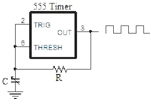
4.3.2 TLC555 Timer
Timer component selection was based primarily on power consumption and bandwidth
specifications. The TLC555 exceeded these and all other requirements for this application. The ‘555’ name actually comes from three 5.0 kΩ resistors that are
combined with transistors and other logic components inside the IC. These internal parts
combine to produce a digital pulse signal for this application. When configured for square wave operation in astable mode, external resistors and capacitors determine the
Figure 4.12: Timer operation diagram
4.3.3 MAX4053 Multiplexer
The MAX4053 multiplexer was selected for the excitation and timer control sub-circuit of Figure 4.7 based on its CMOS construction and low source voltage specifications.
When functioning as a switch, this analog device can be used to combine electrical signals. When provided two different input signals, a third controlling signal can be used
to determine the device’s output. For example, in Figure 4.11 input signals A and B are triangular and square waves, respectively. They will have a common output that is
either A, B, or a combination of the two. This signal output combination is determined
by a third controlling signal, C. In this situation, the time period when signal C is in the ‘on’ mode gives an output that is a portion of the triangular wave (A) and when in the
‘off’ mode, a portion of the square wave (B). The output signal, shown in Figure 4.12, is alternating square and triangular wave half cycles.
4.3.4 74HC74 Flip-Flop
A flip-flop (like D1 or D2 in Figure 4.7) is often used to reduce the frequency of a given square wave. Under basic operation, the clock input determines the value of two outputs,
high (on) or low (off). A square wave clock signal input creates two outputs of that same magnitude but at half frequency or ‘divided by two.’ This occurs because the output high
is only being triggered on every high pulse edge, skipping the mid-cycle low edge in between. Combinations of these devices can be configured to modify the frequencies in different ways, such as dividing a signal by four or eight. Also manufactured using
CMOS technology, the HC7474 is chosen for its low power requirements and adequate bandwidth.
4.3.5 Other Components & Cost
The previously described IC’s were chosen primarily based on function while other
components in the circuit, basic analog devices such as resistors, potentiometers, and capacitors, were selected with cost and availability in mind. Resistors and capacitors come in varying tolerances but the flexibility in circuit design as well as the application
parameters allows use of components without extreme attention to tolerance issues. Just as selection of these components is important to circuit operation, organizing them
together in a way that avoids interference is essential (see section 6.2.6 PCB design).
Electrical costs include the integrated circuits (ICs) and the analog components
5. CDS Circuit Analysis
To analytically ensure that the CDS circuit satisfies the performance requirements for chatter prediction in HSM applications, state equations were derived and PSPICE time-domain simulations were conducted. This chapter highlights the modeling and
simulation process. Simulation results validate the stability and accuracy of the sensor with selected components.
5.1 Overview
Circuit behavior can be analyzed and understood through the derivation and analysis of
dynamic models, the system state equations. These state equations enable the evaluation of gain relations as well as the system’s filtering characteristics. Circuit stability is
analyzed by calculating the system poles from these state equations. Time-domain simulations conducted in PSPICE® further verify circuit performance. The most influential sources of noise and nonlinearity on circuit behavior are then identified and
discussed.
5.2 Circuit Modeling
Kirchoff’s Current Law (KCL) and Kirchoff’s Voltage Law (KVL) can be used to obtain state equations for electrical circuits. To simplify the modeling and analysis, standard
Table.1: Circuit modeling assumptions Ideal square wave excitation
Infinite op-amp input impedance (zero input current) Zero differential input voltage for op-amps
Capacitors C1 and C2 are shorted at carrier frequency
5.2.1 Sensing Circuitry
Operational amplifier A1 of Figure 5.1, which amplifies the signal from the sensing
element, is configured for linear charging with square wave excitation. This linearity is ensured by proper adjustment of the linearity potentiometer, VR1, which causes a
constant gain difference between N2 and N1. Specifically, this adjustment causes the excitation square wave to provide a constant current source to the sensing element, which
through Ohm’s Law is
4 ) ( 1 2
R V VN − N ±
.
Combining Ohm’s Law with KCL at nodes N1, N2, and N3 of Figure 5.1 gives: 0 1 1 3 1 4 2 1 2 1 1 1 = + − + − + + − C j R V V R V V R V R V
VN in N N N N out
ω
( 5.1)
0
2 4
1
2 − + =
N s N
N j C V
R V
V ω
( 5.2)
0 ) 1 ( 8 2 8 6 6 8 2 3 5 3 = + + + + − R sC R R R R C j V R V
VN out N ω
( 5.3)
Realizing that V must equal V to satisfy the ideal operational amplifier assumptions
and capacitor assumptions listed in Table 5.1, the preceding equations can be simplified.
With approximately equal to zero at the excitation frequency of 225kHz, Equation 5.3
reduces to
2
N N3
2 C 6 5 1 R R V V + 2 N
out = or V
2
2 VN
out = ⋅ when R5 =R6. Similarly, C can be
eliminated from Equation 5.1 with capacitor assumptions and substituting for V ,
giving: 1 out 0 2 3 2 1 4 2 1 2 1 1
1 − + + − + − ⋅ =
R V V R V V R V R V
VN in N N N N N
To obtain a meaningful relationship between the sensing element capacitance and the
voltage output in the time domain,
dt dV
C N
s
s = 2
i can be substituted into Equation 5.2.
Then, by manipulating this equation, we obtain
0 1
0 4
1 2
2 =
−
+
∫
dtR V V C V t t N N s
N ( 5.5)
Note that the guarding amplifier, A2, was not taken into consideration for this analysis.
This amplifier is configured as a follower, which means that it forces the guard voltage to
equal the voltage at the sensing element. Since by assumption V equals V , no
current flows between these nodes.
2
N N3
From Equation 5.5, it is clear that the output voltage is directly related to sensing
capacitor displacement because is inversely proportional to plate motion. This is
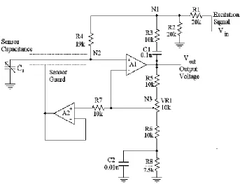
illustrated in Figure 5.2, which shows the linear charging and discharging of C at the
center of one period with the ideal circuit values listed in Figure 5.1. Note that R4 can be adjusted to any value to set the desired output gain and the excitation voltage is +10V and –10V for charging and discharging, respectively at a nominal capacitance of 50 microns.
s C
1.2 1.4 1.6 1.8 2 2.2 2.4 2.6 2.8 3 3.2
x 10-6
-2.5 -2 -1.5 -1 -0.5 0 0.5 1 1.5 2 2.5 Ou pu t ( V )
Time (s)
Voltageout
Figure 5.2: Linear charging/discharging of Cs
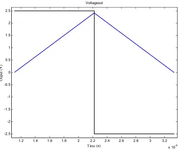
Nonlinear charging results when gain relations described earlier are not satisfied, which is primarily caused by variations in resistance from nominal values. The primary sources of non-adjustable nonlinearity include variations in R1, R2, R3, and output impedance of
the MAX4053 analog multiplexer. When these resistance values differ significantly from those presented in Figure 5.1, nonlinear charging results. An example of this is shown in Figure 5.3, where the value of R1 is changed from 20 kΩ to 20.1 kΩ to show the effect of
a 100Ω change caused by the output impedance from the analog switches S1 and S2.
Note that the plot values are scaled up from the actual 100Ω and a zoomed image with
Figure 5.3: Nonlinear charging/discharging of Cs (red)
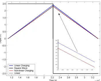
To compensate for inherent circuit nonlinearities, the linearity potentiometer VR1 must be
correctly adjusted. This potentiometer varies the resistance ratio between R5 and R6 to correct for nonlinearities in other parts of the sensing circuitry. Figure 5.4 demonstrates that VR1 adjusts the ratio of R5/R6 appropriately to correct for the nonlinearity in the
Figure 5.4: Adjustment of VR1 to correct charging nonlinearity and gain reduction
The preceding analysis related nodal voltages gains to circuit linearity; by adjusting VR1 for unity gain between N1 and N2, the square wave excitation creates constant current
and therefore linear charging and discharging of the sensing element. The non-inverting feedback combination of R5 and R6 give an approximate gain of 2.0 from sensing
element to output A1 when properly adjusted. Though the RC combination of R8 and C2 has little effect on the sensing element’s gain, it improves stability up to a bandwidth of approximately 2.0 kHz. Any resonance or oscillation at frequencies below this cutoff is
5.2.2 Filtering & Demodulation
The flexibility of this circuit allows for noise filtering at several locations, which is essential for maximizing the SNR. The circuit topology includes first-order low-pass and
high-pass filters as well as synchronous demodulation (Figure 5.5).
Figure 5.5: Demodulation Circuit Schematic
Extending the KCL and KVL circuit analysis to the high and low-pass filters at nodes N4 and N5, respectively, gives:
0 ) ( 9 4 1 4
3 − + =
R V V V C j N A N
ω ( 5.6)
0 12 4 5 5 4 = − + R V V V C
j N N
N
ω ( 5.7)

![Figure 2.3: Out-of-phase cut [39]](https://thumb-us.123doks.com/thumbv2/123dok_us/1342148.1167110/18.612.280.369.75.181/figure-out-of-phase-cut.webp)
![Figure 2.4: Rough surface finish caused by tool chatter [18]](https://thumb-us.123doks.com/thumbv2/123dok_us/1342148.1167110/19.612.237.413.228.403/figure-rough-surface-finish-caused-tool-chatter.webp)