ABSTRACT
KING, MATTHEW RUSSELL. Development of Phase Change Materials for RF Switch Applications. (Under the direction of Jon-Paul Maria and Elizabeth Dickey).
For decades chalcogenide-based phase change materials (PCMs) have been reliably
implemented in optical storage and digital memory platforms. Owing to the substantial
differences in optical and electronic properties between crystalline and amorphous states,
device architectures requiring a “1” and “0” or “ON” and “OFF” states are attainable with
PCMs if a method for amorphizing and crystallizing the PCM is demonstrated. Taking
advantage of more than just the binary nature of PCM electronic properties, recent reports
have shown that the near-metallic resistivity of some PCMs allow one to manufacture high
performance RF switches and related circuit technologies.
One of the more promising RF switch technologies is the Inline Phase Change Switch (IPCS)
which utilizes GeTe as the active material. Initial reports show that an electrically isolated,
thermally coupled thin film heater can successfully convert GeTe between crystalline and
amorphous states, and with proper design an RF figure of merit cutoff frequency (FCO) of
12.5 THz can be achieved.
In order to realize such world class performance a significant development effort was
undertaken to understand the relationship between fundamental GeTe properties, thin film
deposition method and resultant device properties. Deposition pressure was found to be the
deposition process produced GeTe films with a crystalline resistivity of 3 ohm-μm. Upon
implementing these films into IPCS devices, post-cycling morphological analysis was
undertaken using STEM and related analyses.
It was revealed that massive structural changes occur in the GeTe during switching, most
notably the formation of an assembly of voids along the device centerline and large GeTe
grains on either side of the so-called active region. Restructuring of this variety was tied to
changes in ON-state resistance with increasing pulse number, where initially porous and
granular GeTe was converted to large crystalline domains comprising the majority of the RF
gap. A phenomenological model for this morphology was presented in which the OFF pulse
melts a given width of GeTe and upon cooling the crystalline template outside the melt
region acts as a template for an inward-propagating crystalline growth front. This model was
further extended to explain observed morphology for ON pulses. The voids observed along
the device centerline were connected to increasing OFF state resistance and a relatively
stable ON state with increasing pulse number via a series resistance model. As a result of
this analysis, OFF state resistance was suggested as an early indicator of device reliability.
Finally, microstructural and electrical property observations were used as a basis for
implementing improvements to the GeTe deposition process in the form of a heated substrate
platform. It was shown that this provides a viable method for attaining stable as-deposited
GeTe morphology and a substantially improved crystalline resistivity (2 ohm-μm).
Development of Phase Change Materials for RF Switch Applications
By
Matthew Russell King
A dissertation submitted to the Graduate Faculty of North Carolina State University
in partial fulfillment of the requirements for the degree of
Doctor of Philosophy
Materials Science and Engineering
Raleigh, North Carolina 2016
APPROVED BY:
_______________________________ _______________________________
Dr. Jon-Paul Maria Dr. Elizabeth C. Dickey
Materials Science and Engineering Materials Science and Engineering
Committee Co-Chair Committee Co-Chair
_______________________________ _______________________________
Dr. Ramon Collazo Dr. Daryoosh Vashaee
Materials Science and Engineering Electrical and Computer Engineering
DEDICATION
BIOGRAPHY
Matthew Russell King was born in Longview, TX and ultimately raised in Eastern North
Carolina. Having mastered a love of pork and vinegar based barbeque, he attended North
Carolina State University for both his Bachelor of Science and Master of Science degrees.
After completing his M.S. in Materials Science and Engineering in 2009 he began full time
employment at Northrop Grumman Corporation in the Advanced Concepts and Technologies
Division of the Electronic Systems Sector. Located in the microelectronic research and
development facility known as the Advanced Technology Labs, Matthew was involved in
bulk synthesis of halide compounds for radiation detectors; synthesis and fabrication of
nanowire-based photodetectors; MOCVD growth of III-nitride films for high frequency
electronic devices; chalcogenide phase change material deposition and fabrication for RF
switch development; and a wide variety of other materials development efforts. During his
full time employment at NGC Matthew resumed his studies at NC State in pursuit of a PhD
in Materials Science and Engineering, at which point he worked alongside NGC colleagues
and remotely with Dr. Jon-Paul Maria and Dr. Elizabeth Dickey to study the relationship
between chalcogenide phase change material properties and attainable RF switch
ACKNOWLEDGMENTS
First and foremost I must acknowledge and express my thanks to NC State advisors Dr.
Jon-Paul Maria and Dr. Elizabeth Dickey. This was an unconventional degree program, to be
sure, and I appreciate you making this a reality. I appreciated your input and guidance
throughout the course of this process.
I am beyond grateful to Dr. Robert Young at Northrop Grumman. His persistent, thoughtful
and logical approach to problem solving in the face of many, many technical and
programmatic challenges has shaped my outlook greatly. His specific guidance during this
program was invaluable. The Phase Change Switch technical team at NGC deserves more
praise than I am capable of offering—I have never worked with such a talented, tenacious
and creative group of people and I’m positive without you I would not be where I am today.
Nabil El-Hinnawy in particular played a critical role in expanding my knowledge of
processing and device physics (among many other things) and to him I’m forever indebted.
The rest of the PCS team helped keep me honest and pushed me to understand materials
research in the context of a much larger application space—Pavel Borodulin, Brian Wagner,
Evan Jones, Andy Ezis, Carlos Padilla, Colin Furrow, Kate Malachowski, Doyle Nichols and
Mike Lee, I appreciate all of you. The technical staff in the ATL microelectronics facility
deserves much praise as well; without them we would not have the IPCS.
There were many other technical advisors at ATL who supported my continuous technical
Berghmans, Dr. Narsingh Singh, Dr. David Knuteson, David Kahler, Dr. Victor Veliadis, Dr.
Tom Ambrose, thank you! I must also thank the NGC management for allowing me to
pursue this degree and continuously affirming its value—John Fusco, Dr. Hong Zhang, Mike
Lee, Sandro Di Giacomo, Dr. Nicholas Paraskevopoulos, Tim Patterson and Dennis Fortner,
I am grateful for your support.
Of course I would not have pursued this degree in the first place if not for a history of superb
scientific advisors, perhaps most importantly Dr. Jerry Cuomo, Dr. Richard Guarnieri and
Dr. Chris Oldham. I would not be where I am today without you!
Someone who never expects acknowledgement or receives enough of it is Edna Deas in the
NCSU MSE department. She has helped me on more occasions than I care to mention in
departmental administrative tasks and without her I would likely have not been allowed to
finish. Thank you Edna!
I am deeply thankful for my loving and supportive family—my parents and my siblings
Christopher, Nick and Emily, thank you for allowing me to be myself all these years.
I want to also thank my son Charlie, who doesn’t know it yet but helped me write every line
on these pages.
Finally, perhaps most of all, I want to thank my love, my wife, Amy. You lift me higher
TABLE OF CONTENTS
LIST OF TABLES ... viii
LIST OF FIGURES ... ix
1 Introduction ... 1
1.1 Chalcogenide Based Phase Change Materials ... 1
1.1.1 Bonding in PCMs ... 2
1.1.2 Impacts of Resonant Bonding ... 8
1.1.2.1 Structural Properties of Prototypical PCM GeTe ... 8
1.1.2.2 Optical Properties of PCMs ... 12
1.1.2.3 Thermal Properties of PCMs ... 15
1.1.2.4 Electronic Properties of PCMs ... 22
1.1.3 The Phase Change Process... 30
1.2 Applications of Phase Change Materials ... 37
1.2.1 Optical Storage... 37
1.2.2 Non-Volatile Digital Memory... 38
1.2.3 RF Electronic Switches ... 46
1.2.3.1 The Inline Phase Change Switch ... 49
1.3 Summary of Scope ... 55
2 Experimental Methodology ... 57
2.1 Phase Change Material Deposition ... 57
2.2 Phase Change Material Characterization ... 60
3 Development of the GeTe Deposition Process ... 68
3.1 Abstract ... 68
3.2 Introduction ... 69
3.3 Experimental ... 70
3.4 Results and Discussion ... 72
3.5 Conclusions ... 82
3.6 Acknowledgements ... 82
4 Morphological Analysis of GeTe in 1st Generation Inline Phase Change Switches ... 84
4.1 Abstract ... 85
4.2 Introduction ... 85
4.3 Experimental ... 89
4.4 Results and Discussion ... 90
5 Morphological Analysis of GeTe in 2nd Generation Inline Phase Change
Switches ... 106
5.1 Introduction ... 106
5.2 Experimental ... 109
5.3 Results and Discussion ... 115
5.4 Conclusions ... 141
6 Development of an Improved GeTe Deposition Process ... 143
6.1 Introduction ... 143
6.2 Experimental ... 144
6.3 Results and Discussion ... 145
6.4 Conclusions ... 166
7 Conclusions and Future Directions... 168
7.1 Conclusions ... 168
7.2 Future Directions ... 169
LIST OF TABLES
Table 1.1. Optical properties of selected group IV, III-V and IV-VI compounds.14,28 ... 12
Table 3.1. Summary of deposition conditions and resultant electrical properties for sputtered GeTe films. ... 73
Table 4.1. Summary of pulse parameters and state of IPCS devices prior to AC-STEM imaging. ... 90
Table 5.1. List of devices and associated pulsing parameters ... 113
Table 5.2. Instrument settings for the Hitachi HD-2300 STEM. ... 114
Table 5.3. Instrument settings for the Hitachi HD2700 AC-STEM. ... 114
Table 5.4. Parameters for resistance model of pulsed, ON IPCS. ... 123
Table 5.5. Parameters for resistance model of as-fabricated, ON IPCS. ... 123
Table 5.6. Parameters for resistance model of pulsed, OFF IPCS. ... 126
LIST OF FIGURES
Figure 1.1. Common cations and anions which form the backbone of phase change materials. ... 2
Figure 1.2. Energy difference between rocksalt and chalcopyrite structures for Au(In,Sn,Sb)Te2, Ag(In,Sn,Sb)Te2 and Cu(In,Sn,Sb)Te2 PCMs as a function
of the number of valence electrons.16 ... 4
Figure 1.3. A map of phase change materials relating hybridization and ionicity. (a) Compounds from specific chalcogens tend to form co-located groups where increasing atomic number is found closer to the origin. (b) An expanded view of the Te and Sb-based compound section shows minimal hybridization and ionicity.8 ... 6
Figure 1.4. (001) slices of the elemental Sb structure where the left and right schemes represent possible bonding configurations given the number of available bonding electrons. The center figure depicts a resonant bonding scheme in which available electrons are shared between Sb atoms.14 ... 7
Figure 1.5. Crystal structure of GeTe arranged in the (a) cubic and (b) hexagonal framework.18 ... 10
Figure 1.6. Representative structural motif of a-GeTe including both tetrahedral and octahedral fragments.24 ... 11
Figure 1.7. Infrared reflectance spectra for amorphous and crystalline Ge1Sb2Te4 (dashed
lines modeled, solid lines measured). Text indicates optical signatures of various contributions in both states.14 ... 13
Figure 1.8. Calculated, normalized thermal conductivity of selected III-V (covalently bonded) and IV-VI (resonantly bonded) compounds.33 ... 16
Figure 1.9. (a) Thermal conductivity as a function of temperature for several III-V and IV-VI compounds. (b) Cumulative normalized thermal conductivity as a function of phonon mean free path for the same group of materials.33 ... 17
Figure 1.10. Experimentally measured thermal conductivity as a function of electrical conductivity for various (GeTe)x(Sb2Te3)1-x alloys. A curve depicting the
Figure 1.11. Modeled electron density and polarization for NaCl (a,c) and PbTe (b,d), indicating electron delocalization and polarization effects of 2nd, 3rd and 4th nearest neighbors.33 ... 20
Figure 1.12. Thermal conductivity as a function of annealing temperature for various (GeTe)x(Sb2Te3)1-x alloys.35 ... 21
Figure 1.13. (a) Germanium vacancy concentration and (b) Fermi level as a function of temperature for Ge-rich and Te-rich conditions.46 ... 24
Figure 1.14. Transport properties of GeTe as a function of temperature for various deposition temperatures.38 ... 26
Figure 1.15. Normalized cell resistance and threshold voltage (Vth) as a function of time
for an a-PCM.53 ... 28
Figure 1.16. Classical nucleation scheme showing Gibbs free energy as a function of nuclei radius comparing homogeneous and heterogeneous nucleation processes. Curves expressing surface and volume free energy terms are included for reference. ... 32
Figure 1.17. Generalized PCM time-temperature-transformation (TTT) diagram (left) atomic mobility (center) and driving force for crystallization (right) as a function of temperature.1 ... 33
Figure 1.18. Viscosity as a function of reciprocal temperature normalized to the glass transition temperature (Tg) for a variety of materials.67 ... 34
Figure 1.19.Crystal growth velocity of GeTe as a function of temperature, measured directly via transmission electron microscopy.69 ... 35
Figure 1.20. Relationship between the temperature at which maximum growth rate occurs (Tmax) and the glass transition temperature (Tg) for various materials.
The Tmax/Tg ratio is consistently 1.48±0.15 for all studied materials.63 ... 36
Figure 1.21. Schematic ternary diagram identifying important PCM compounds and related optical storage media technology nodes.7 ... 38
Figure 1.22. (a) Schematic of a PCM memory cell. Fabricated cell in the (b) ON/SET/crystalline state and (c) OFF/RESET/amorphous state.70 ... 39
Figure 1.24. Variation in electrical resistance with temperature for GeTe showing the transition from the amorphous (resistive) to crystalline (metallic) state. Data from71, model from60. ... 41
Figure 1.25. PCM cell resistance for an increasing number of cycles, demonstrating reliability up to 1012 cycles.70 ... 45
Figure 1.26. Insertion loss (left) and isolation (right) for a variety of RF switch technologies.85 ... 47
Figure 1.27. Simplified picture of an arbitrary reconfigurable RF circuit which integrates a collection of amplifiers and filters to demonstrate wideband performance. ... 49
Figure 1.28. Schematic layout of the inline phase change switch (IPCS) from the (a) top view and (b) cross section view, along the dotted line in (a). ... 51
Figure 1.29. Ge-Sb-Te ternary phase diagram with the (GeTe)x(Sb2Te3)1-x tie line
identified. Compositional dependencies of switching speed and OFF state stability (i.e. increasing Tcryst) are shown. GeTe is indicated as the lowest
resistivity PCM composition. ... 54
Figure 2.1. Schematic of experimental magnetron sputtering system. ... 57
Figure 2.2.Scattering geometry of RBS experiments performed at Evans Analytical Group. ... 63
Figure 3.1. Normalized resistance [R(T)/Rmax] as a function of temperature for GeTe
films sputtered at a variety of power and pressure conditions. (b) Expanded dotted line region in Figure 1(a) to show transition temperatures and final RON values. ... 72
Figure 3.2. Oxygen content (top) and deposition rate (bottom) of GeTe films as a function of deposition pressure and power. Oxygen incorporation was reduced to negligible levels with a 10 min pre-sputter process at 65 W and 5 mTorr. ... 74
Figure 3.3. Optical emission spectroscopy of the DC magnetron discharge at 65 W and 5 mTorr. The inset shows the absence of the oxygen triplet at 777 nm indicating gaseous oxygen is not present in the discharge. ... 75
Figure 3.4. Morphology of GeTe films as-deposited and post-crystallization, as a function of deposition pressure. Scale bars 500nm. ... 77
exhibit no crystalline reflections. Films deposited at 17 mTorr consist of GeO2 and TeO2 phases in the as-deposited state. ... 79
Figure 3.6. TLM measurements of crystalline GeTe sputtered at 65 W and 5 mTorr. Calculated Rc and ρcryst are 9.85x10⁻³ Ω-mm and 2.97x10⁻³ Ω-mm,
respectively. ... 81
Figure 4.1. Cross-sectional AC-STEM image of the as-fabricated IPCS device A. Insets represent NBD data from the associated symbols. Scale bar 300nm. ... 91
Figure 4.2. AC-STEM image of IPCS device B pulsed at MPA and left ON. Insets represent NBD data from the associated symbols. Scale bar 200nm. ... 93
Figure 4.3. EDS line scan of IPCS device E through the apex of the thin film heater. ... 94
Figure 4.4. AC-STEM image of IPCS device C pulsed at MPA and left OFF. Insets represent NBD data from the associated symbols. Scale bar 200nm. ... 96
Figure 4.5. AC-STEM image of IPCS device D pulsed at 3% below MPA and left OFF. Insets represent NBD data from the associated symbols. Scale bar 200nm. ... 97
Figure 4.6. AC-STEM image of IPCS device E pulsed at 15% above MPA and left OFF. Insets represent NBD data from the associated symbols. Scale bar 200nm. ... 99
Figure 4.7. STEM images of the interface between the active area and transition region for a device in the (a) ON and (b) OFF state. Scale bars 10nm. ... 100
Figure 4.8. Histograms of crystallite diameter for specified pulse conditions, where n is the total number of measured crystallites. ... 101
Figure 4.9. Proposed model for (a) melting and (b) solidification of GeTe in the IPCS device architecture during an OFF pulse (image is device C). Dotted lines representing the melt front were predicted using the modeling tool described in Ref 90 for times (progressing from inner to outer) of 40, 50, 60, 80, and 100ns, while the recrystallization lines are a qualitative representation of propagating crystal growth fronts resulting in a quenched central amorphous region smaller than the full melt zone. ... 102
Figure 5.1. Cross sectional dark field TEM image of as-fabricated 2nd generation IPCS devices with relevant layers identified. ... 108
Figure 5.2. Optical image of the 0.9x30μm IPCS device studied herein. ... 109
Figure 5.4. Cross-sectional STEM showing the perspective seen in plan view STEM images, where the image direction is through the GeTe thickness and the foil (blue dotted line) is composed of a Si3N4/GeTe/Si3N4 sandwich. ... 112
Figure 5.5. Device resistance as a function of pulse number for samples listed in Table 5.1. ... 116
Figure 5.6. SEM image during FIB preparation, in which the bottom of the W heater is exposed along with GeTe on either side of the heater. Asterisks indicate examples of preexisting voids in the GeTe layer. ... 117
Figure 5.7. In-process SEM images of FIB sections viewed from the (a) bottom and (b) top of the IPCS device. Voids directly above the W heater are observed while none are seen at the top of the GeTe. ... 118
Figure 5.8. Transmitted electron (TE) STEM images of plan view prepared IPCS devices with OFF pulse conditions indicated for each image. ... 120
Figure 5.9. Higher magnification TE STEM images of the samples in Figure 5.8. ... 121
Figure 5.10. Identification and relative size of 3 major regions in the IPCS device: active region, transition region and as-fabricated GeTe. ... 122
Figure 5.11. Effect of reduced cross sectional area (voiding) in the active region on ON-state GeTe channel resistance. ... 125
Figure 5.12. Effect of reduced cross sectional area (voiding) in the active region on OFF-state GeTe channel resistance. ... 127
Figure 5.13. Proposed model for melting, grain growth and quenching during an OFF pulse, mapped against a modeled thermal profile for the IPCS. ... 129
Figure 5.14. EDS elemental mapping for O, Si, Ti, Ge, Te and Pt for the MPA+5% amorphous state device. Top-most image is the original STEM image of the analyzed area. ... 131
Figure 5.15. Comparison between (a) MPA+5% and (b) MPA+15% OFF state morphology via TE mode AC-STEM. ... 133
Figure 5.16. Comparison between (a) MPA+5% and (b) MPA+15% ON state morphology via TE mode AC-STEM. ... 135
Figure 5.18. TE AC-STEM image of (a) OFF and (b) ON state morphology for MPA+5% OFF pulse. ... 137
Figure 5.19. MPA+5% at 2x RON sample where (a) substantial curtaining and mass thickness issues are seen in SE STEM mode and (b) subsequent TE AC-STEM analysis is obscured. ... 138
Figure 5.20. (a) OFF state TE AC-STEM image for MPA+5%. (b) Higher magnification image of the selected region. (c) SEM image of a blanket GeTe film after crystallization. ... 141
Figure 6.1. X-ray reflectivity data of (a) amorphous and (b) crystalline GeTe as a function of deposition pressure. ... 146
Figure 6.2. SEM analysis of a-GeTe and c-GeTe morphology as a function of deposition pressure. All scale bars 500nm. ... 149
Figure 6.3. Effect of deposition pressure on (a) germanium, (b) oxygen and (c) argon content in amorphous and crystalline GeTe films. ... 151
Figure 6.4. Te:Ge sputter yield ratio as a function of ion energy and angle.124 ... 152
Figure 6.5. SEM images of GeTe films deposited at various substrate temperatures and annealed at 280°C for 2hrs. Samples are viewed at an angle on a cleaved edge. Scale bars 1μm. ... 156
Figure 6.6. GIXRD data for GeTe films deposited at various substrate temperatures and annealed at 280°C for 2 hours. Data sets are shifted vertically for ease of comparison. Relevant GeTe reflections are identified. ... 159
Figure 6.7. GeTe resistivity as a function of deposition temperature, before and after annealing at 280°C for 2 hours. ... 160
Figure 6.9. (a) Cross sectional DF-TEM image of a 2nd generation IPCS device using the baseline GeTe deposition process, where cracks are observed over the W heater. (b) Cross sectional SEM image of an IPCS device with the improved GeTe deposition process, where no cracks are observed in the GeTe layer. Scale bars 200nm. ... 162
Figure 6.10. RON as a function of pulse number for IPCS devices with heated and
unheated GeTe deposition processes. ... 164
1
Introduction
1.1
Chalcogenide Based Phase Change Materials
It has been known for decades that a selection of compounds based on a group VI anion
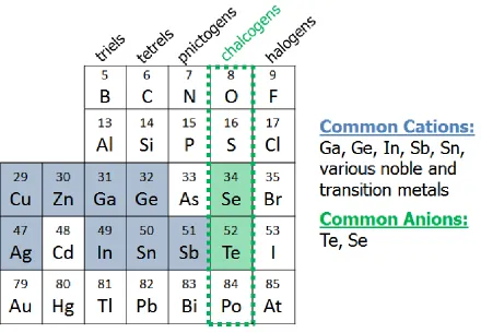
sublattice—that is, chalcogenides—have a wide array of unique material properties.1,2
Commonly employed elements for relevant compounds are shown in Figure 1.1.
Chalcogenides of various compositions have been shown to be superconducting3,
ferroelectric4 and thermoelectric5, and some have recently been identified as topological
insulators6. To date, the most technologically useful aspects of this class of materials,
however, are derived from the differences between their amorphous and crystalline states. In
particular, both the optical and electrical properties of these materials are remarkably
different depending on their structural framework or phase1,7,8. This is the origin of the
commonly used term phase change material (PCM). The question of how these materials are
able to sustain such an extensive array of properties continues to be an area of vibrant
research, even after nearly 50 years7,9–11. Given that our understanding of PCM physics is
continuously evolving, the following section will summarize the state of the field as it stands
today. This foundation will then be used to identify important technological thrusts which
Figure 1.1. Common cations and anions which form the backbone of phase change materials.
1.1.1
Bonding in PCMs
As is the case for all classes of materials, the aforementioned PCM properties originate from
a specific, and in the case of inorganic materials a somewhat unique, bonding modality. The
most commonly encountered global bonding types are metallic, ionic and covalent; however,
all PCMs exhibit a type of minimally mixed covalent-ionic character referred to as “resonant
bonding”.7 Resonant bonding has been noted in a variety of semiconductor materials12,13 but
Beginning with more commonly encountered bonding types, both covalent and ionic bonding
are characterized by strong electron localization, whether in the form of hybridized orbitals
for the former, or electron exchange interactions for the latter. Atomic and electronic
processes in these materials, then, tend to be influenced primarily by first nearest neighbor
effects where electron distribution perturbations are confined to locally coordinated atoms.
Furthermore, bonding between s-block and p-block elements typically obey the octet rule in
which a stable configuration of 8 valence electrons per atom is observed.
As a point of contrast, elemental Sb is often used as an exhibition of how PCM resonant
bonding departs from these characteristics seen ionic and covalent bonding8,14,15. The
electronic configuration of antimony—[Kr]4d105s25p3—exhibits a filled s-orbital and 3
available p-orbital electrons which can participate in bonds. Furthermore, antimony adopts a
6-fold coordinated octahedral structure, which is fairly over-coordinated (alternatively,
“hypervalent”) considering the number of available bonding electrons. Through DFT studies
of energetically favorable PCM structures, Luo et al. 16 previously showed that viable phase
change materials almost exclusively show a proclivity toward the 6-fold coordinated rocksalt
structure rather than the 4-fold coordinated chalcopyrite structure. Comparing the
configurational energy between the two structures for a variety of PCMs (∆𝐸𝐸= 𝐸𝐸𝑜𝑜𝑟𝑟𝑜𝑜𝑟𝑟𝑘𝑘𝑘𝑘𝑘𝑘𝑘𝑘𝑘𝑘−
𝐸𝐸𝑜𝑜𝑟𝑟ℎ𝑘𝑘𝑘𝑘𝑟𝑟𝑜𝑜𝑎𝑎𝑎𝑎𝑟𝑟𝑎𝑎𝑘𝑘𝑎𝑎) it was found that the rocksalt structure was energetically favorable if the
Figure 1.2. Energy difference between rocksalt and chalcopyrite structures for
Au(In,Sn,Sb)Te2, Ag(In,Sn,Sb)Te2 and Cu(In,Sn,Sb)Te2 PCMs as a function of the number
of valence electrons.16
To further generalize a method for identifying viable PCMs based exclusively on bonding,
Lencer et al.8 created a “treasure map” which relates ionicity and hybridization and found
that all PCMs fell within a very specific region (Figure 1.3). Using the work of
Littlewood12,13,17 as a foundation, ionicity and hybridization relate the radii of valence
electron s- and p-orbitals between anions and cations for candidate compounds. Ionicity is
defined as 𝑟𝑟𝜎𝜎′ =𝑟𝑟𝑎𝑎𝑘𝑘𝑎𝑎𝑎𝑎𝑜𝑜𝑎𝑎− 𝑟𝑟𝑎𝑎𝑟𝑟𝑘𝑘𝑘𝑘𝑎𝑎𝑜𝑜𝑎𝑎, where the difference in anionic and cationic p-orbital radii can be related to the more conventional measure of ionicity, i.e. the electronegativity
as 𝑟𝑟𝜋𝜋−1 =��𝑟𝑟𝑎𝑎𝑘𝑘𝑎𝑎𝑎𝑎𝑜𝑜𝑎𝑎 − 𝑟𝑟𝑘𝑘𝑘𝑘𝑎𝑎𝑎𝑎𝑜𝑜𝑎𝑎�+�𝑟𝑟𝑎𝑎𝑟𝑟𝑘𝑘𝑘𝑘𝑎𝑎𝑜𝑜𝑎𝑎− 𝑟𝑟𝑘𝑘𝑟𝑟𝑘𝑘𝑘𝑘𝑎𝑎𝑜𝑜𝑎𝑎��−1, where the differences in valence s- and p-orbital radii for anion and cation species provide a measure of tendency toward orbital
hybridization. Moving away from the origin along either axis in Figure 1.3, one quickly
leaves the area of viability for PCMs. Importantly, as stated previously, one finds a tendency
for strong electron localization in either the highly ionic or highly hybridized cases. As such,
understanding how this unique bonding modality originates will provide a means of
Figure 1.3. A map of phase change materials relating hybridization and ionicity. (a)
Compounds from specific chalcogens tend to form co-located groups where increasing
atomic number is found closer to the origin. (b) An expanded view of the Te and Sb-based
(a)
Returning to the example of antimony, Figure 1.4 shows schematic (100) slices of an Sb
crystal, where the left and right images portray possible bond arrangements. In both cases,
each Sb atom is surrounded by typical 2-electron covalent bonds which prevent a fully
bonded octahedral arrangement from occurring.
Figure 1.4. (001) slices of the elemental Sb structure where the left and right schemes
represent possible bonding configurations given the number of available bonding electrons.
The center figure depicts a resonant bonding scheme in which available electrons are shared
between Sb atoms.14
A more energetically favorable configuration (Figure 1.4, center) is one in which electrons
are delocalized and in a state of resonance about each Sb atom14. By virtue of this
delocalization, the state of each Sb atom depends not just on next-nearest neighbors—as is
found in most covalently bonded materials—but on second, third and fourth nearest
neighbors as well. As such, resonantly bonded structures are highly susceptible to disruption
via alloying, strain effects, dislocations and point defects—any electronic or structural
is important for PCMs because even a small amount of disorder can facilitate major changes
in observed material properties. In fact, technologically viable applications of PCMs are
founded entirely on reliably cycling PCMs between the ordered crystalline state and a
disordered, often amorphous state.
1.1.2
Impacts of Resonant Bonding
Before addressing the mechanisms with which PCMs are converted between crystalline and
amorphous states, important impacts of resonance bonding will be discussed. Given the
focus of this dissertation, optical properties will be very briefly discussed while structural,
thermal and electrical properties will be discussed in detail.
1.1.2.1
Structural Properties of Prototypical PCM GeTe
There are many structural nuances which are observed for various PCM alloy compositions;
however the discussion here will be restricted to prototypical PCM GeTe. This is for the
sake of simplicity, but also because GeTe is the exclusive PCM utilized in this body of
research. As mentioned in section 1.1.1, one common feature of PCMs is the distorted
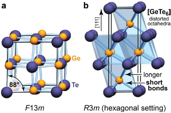
rocksalt-like structure. The stable room temperature phase of GeTe (α–GeTe) can be
characterized as having alternating cation and anion layers stacked along [111], but in a
departure from the true cubic structure, two distinct Ge-Te bond lengths are observed. This is
the basis of a rhombohedral distortion in the form of a shift in the primary unit cell angle
are converted from being periodic to stochastic in nature19. GeTe congruently melts at 998K
and in the solid state a relatively wide compositional phase space (~10 at%) exists for what is
nominally the 1:1 GeTe stoichiometry. Moving back to local bond arrangements, as a means
of lowering the overall crystal energy, long and short bonds alternate along [111] in what is
generally known as a Peierls distortion14,19. As another means of lowering the free energy of
the system7,20, crystalline α-GeTe presents an anomalously large number of Ge vacancies, in
the range of 8-10%21,22. This results from the tendency for structural relaxation away from
the rocksalt structure and annihilation of unfavorable antibonding Ge-Te states7. In order to
maintain stoichiometry, local Ge vacancies in c-GeTe lead to segregation of a
“quasi-amorphous” Ge phase collected at grain boundaries22. It will be seen in subsequent sections,
particularly Section 1.1.2.4, that these Ge vacancies are absolutely critical for characteristic
metallic-like conductivity observed in GeTe and are therefore the basis of many important
Figure 1.5. Crystal structure of GeTe arranged in the (a) cubic and (b) hexagonal
framework.18
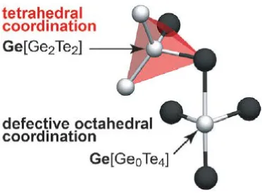
The commonly encountered disordered state of GeTe is similar to c-GeTe in that a
substantial number of octahedrally coordinated fragments remain7,23. In contrast to c-GeTe,
however, tetrahedrally coordinated units predicated on Ge-Ge homopolar bonds are also
observed (Figure 1.6)24. Kolobov et al.25 estimated that two thirds of Ge atoms retain
octahedral coordination, while the remaining one third take on a tetrahedrally coordinated
motif. Recalling the discussion of resonance from Section 1.1.1, a decrease in coordination
leads to an increase in the covalent character of the bond distribution and a concomitant
hyper-localization of bonding electrons. Furthermore, as is typical of amorphous glasses,
short range order in the form of tetrahedral and octahedral subunits have no long range
amorphous narrow gap semiconductor1,7,18 with very few remnant characteristics unique to
c-GeTe. Among the differences between the two states, a substantial increase in atomic
density is observed in the crystalline state, on the order of 8-12%26,27. Building on the
discussion of the considerable structural differences between a-GeTe and c-GeTe, resultant
material properties will be discussed in Sections 1.1.2.1-1.1.2.4.
Figure 1.6. Representative structural motif of a-GeTe including both tetrahedral and
1.1.2.2
Optical Properties of PCMs
One immediate outcome of electron delocalization is the substantial electronic polarizability
observed in crystalline PCMs. As an extension, spectroscopic reflectivity analyses by
Shportko et al.14 indicate PCMs have both a large optical dielectric constant and fairly
narrow band gaps (Table 1.1). Littlewood also noted this as a general feature of many IV-VI
cubic compounds12,13.
Table 1.1. Optical properties of selected group IV, III-V and IV-VI compounds.14,28
Material Optical Dielectric Constant, ε∞ Optical Gap, Eg (eV)
Si 11.9 1.12
Ge 16.2 0.66
GaAs 10.9 1.42
GaN 5.4 3.4
Ge1Sb2Te4 36.2 0.39
Ge2Sb2Te5 33.3 0.48
GeTe 33.2 0.55
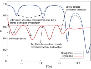
Quite interestingly, substantial differences in the reflectivity spectra—which originate from
contributions from the index of refraction, Drude oscillations, dielectric constant, optical gap
and sample thickness—can be seen when comparing the crystalline and amorphous states
(Figure 1.7). Based on the earlier discussion of PCM bonding, this difference can be
understood in the context of order and disorder. If polarizability and the optical dielectric
constant rely on electron delocalization (resonant bonding), then disruptions to long- or even
medium-range order can effectively alter these properties. Studies of amorphous PCMs19,23–
25,29–31
loss of complete octahedral coordination in all or part of the cation sublattice in favor of
tetrahedral coordination (e.g. tetrahedral Ge-Ge bonds in a-GeTe24). Discussions in
subsequent sections will further demonstrate how the presence or absence of resonance
control critical material properties in PCMs.
Figure 1.7. Infrared reflectance spectra for amorphous and crystalline Ge1Sb2Te4 (dashed
lines modeled, solid lines measured). Text indicates optical signatures of various
contributions in both states.14
(reflective) or amorphous (less reflective) material32. Comparing these states in other
semiconductors such as Si or Ge, one does not find similar differences in the optical
properties31. This is due to the fact that both amorphous and crystalline states still favor a
local bonding environment which is tetrahedral in nature—that is, strong electron localization
is found even if long range order is not present.
The spectroscopic signatures of PCMs, having their origins in the resonant bonding structural
motif, provide a means of evaluating the degree of resonance in a particular material.14
Specifically, the ratio of optical dielectric constants between crystalline and amorphous
states, 𝜁𝜁= [𝜖𝜖∞𝑟𝑟⁄𝜖𝜖∞𝑘𝑘]−1, and the ratio of optical band gaps, 𝛾𝛾 =𝐸𝐸𝑔𝑔𝑘𝑘𝑎𝑎𝑘𝑘 ⁄𝐸𝐸𝑔𝑔𝑘𝑘𝑎𝑎𝑟𝑟 , indirectly represent the extent to which resonance is affecting observed optical properties. Upon
calculating ζ for common PCMs one finds large values14
—Ge2Sb2Te5 (1.1), GeTe (1.5),
Ge1Sb2Te4 (1.2). While analyses such as x-ray absorption fine structure (EXAFS) can
provide more detailed structure and bonding information, the optical analysis described
above is an excellent “lab grade” method for determining resonant character in a candidate
material. Since resonant bonding affects many material properties, having an easily
obtained, quantitative metric for this characteristic allows one to quickly evaluate candidate
1.1.2.3
Thermal Properties of PCMs
Resonant bonding not only has a significant effect on PCM optical properties, it also controls
PCM thermal conductivities. Most, if not all, PCM-based technologies to date rely on
thermal energy to successfully switch between crystalline and amorphous states; hence a
discussion of the foundation of PCM thermal properties is warranted.
Most IV-VI compounds, including PCMs such as GeTe and SnTe, are known to have quite
low thermal conductivities5,33–37. This is fortuitous in a sense because deeply scaled, high
density optical and digital memory devices would be impractical if not for extreme
localization of thermal energy during a switching pulse. Many crystalline PCMs also have
high, near metallic, electrical conductivities5,38. A number of questions follow: What is the
origin of these properties? Also, if many PCMs exhibit metal-like electrical conductivity,
why don’t they have an equally large thermal conductivity? This section addresses thermal
conductivity in PCMs, while electrical conductivity will be addressed in Section 1.1.2.4.
In an effort to contextualize the relatively low thermal conductivities found in resonantly
bonded materials, Lee et al. [ref Lee 2014] modeled thermal conductivity as 𝜅𝜅=𝐵𝐵 ∙
��𝑀𝑀�𝑛𝑛1/3𝛿𝛿𝜃𝜃3� 𝛾𝛾⁄ �2 , where B is a numerical coefficient, 𝑀𝑀� is the average atomic mass, n is
the number of phonon branches, δ3 is the average atomic volume, θ is the acoustic Debye
temperature, and γ is the Gruneisen parameter. Comparing the thermal conductivities of
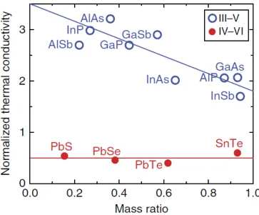
few striking differences (Figure 1.8)33. First, the chosen III-V compounds are all
substantially more thermally conductive, as much as a factor of 5 in some cases. Second,
there is a strong mass ratio dependence for III-Vs, while IV-VI compounds remain mostly
immune to this variable. This disparity is further exhibited across a wide temperature range
Figure 1.9a.33
Figure 1.8. Calculated, normalized thermal conductivity of selected III-V (covalently
Figure 1.9. (a) Thermal conductivity as a function of temperature for several III-V and IV-VI
compounds. (b) Cumulative normalized thermal conductivity as a function of phonon mean
free path for the same group of materials.33
By expressing thermal conductivity as an accumulation of phonon modes and respective
mean-free paths (Figure 1.9b)33, it becomes clear that the heart of this characteristically poor
thermal transport is tied to phonon scattering mechanisms. Indeed, first principle analyses
show the presence of low frequency transverse optical (TO) and longitudinal optical (LO)
phonon states specific to PCMs33,39. In addition to these “soft” phonon modes, point defects
in the form of cation vacancies serve as another substantial scattering mechanism35,39.
Interestingly, vacancy ordering in certain PCM compounds leads to an increase in thermal
conductivity via an overall reduction in this scattering mechanism. However, the overall
thermal conductivity is still substantially lower than one would expect from exclusively
metallic materials where electronic and thermal transport are directly related. The
relationship between electrical and thermal conductivity is theoretically described by the
Wiedemann–Franz law, in which thermal conductivity 𝜅𝜅= 𝜎𝜎𝐿𝐿0𝑇𝑇, where σ is electrical conductivity, T is temperature and L0 is the Lorenz number with a theoretical value of
2.45x10⁻⁸ WΩK-2. The extent to which the thermal conductivity of a material obeys this
relationship can be qualitatively interpreted as a tendency for lattice conduction versus
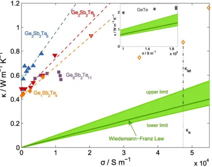
carrier-mediated thermal transport. Siegert et al.35 analyzed a group of (GeTe)x(Sb2Te3)1-x
alloys to determine the effect of composition and order/disorder on thermal conductivity.
When moving along the tie line toward the Sb2Te3 end member, the authors found an
increasing deviation from the Weidemann-Franz law, or, alternatively stated, an increase in
the tendency for lattice conduction (Figure 1.10). It is with these materials the observation of
increased thermal conductivity with annealing temperature—ascribed to reduced point defect
scattering via vacancy ordering—was made35. The other end member, GeTe, which does not
possess a tendency for vacancy ordering, exhibits a greater tendency for carrier based thermal
transport. One must again note, though, that even though GeTe is both the most electrically
and thermally conductive of the (GeTe)x(Sb2Te3)1-x alloys, at ~ 2 W/m-K it is still a quite
Figure 1.10. Experimentally measured thermal conductivity as a function of electrical
conductivity for various (GeTe)x(Sb2Te3)1-x alloys. A curve depicting the Wiedemann-Franz
law is also plotted for reference, with variations in the Lorenz number providing an upper
and lower limit. Data for GeTe is shown in the inset.35
Bringing this analysis full circle, it has been shown that resonant bonding at the same time
engenders electron delocalization, enhanced polarizability, and near-metallic electrical
conductivity, but also critically dampens phonon modes and causes phonon scattering via
point defects33,35,39. Comparing an ionic material such as NaCl to a resonantly bonded
neighbor interactions can be seen. This ultimately gives rise to strong anharmonicity, driven
by previously described soft TO modes, and substantially reduced phonon lifetimes. As
such, the link between resonant bonding and critical material properties continues to be
important.
Figure 1.11. Modeled electron density and polarization for NaCl (a,c) and PbTe (b,d),
indicating electron delocalization and polarization effects of 2nd, 3rd and 4th nearest
neighbors.33
Until now the discussion has focused on PCMs in general but it is important to note that
thermal conductivity in the crystalline and amorphous state can be quite different, and this
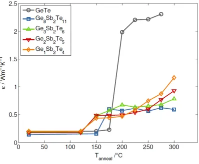
difference depends heavily on composition5,33,35,40. Figure 1.12 shows the thermal transport
properties of various (GeTe)x(Sb2Te3)1-x alloys, where a significant increase in conductivity
occurs at some annealing temperature for all samples. This phenomenon is related to PCM
crystallization which usually occurs in the range of 125-225°C. Amorphous glasses are
(a)
(b)
(c)
known to have generally poor thermal conductivity, as are amorphous semiconductors. In
both cases, severe disruption of long range order is the cause.
Figure 1.12. Thermal conductivity as a function of annealing temperature for various
(GeTe)x(Sb2Te3)1-x alloys.35
Microstructure can also play a large role in PCM thermal conductivity, as is seen when
comparing the bulk (6 W/m-K)37 and thin film (2 W/m-K)35 values for GeTe. Furthermore,
can facilitate in-plane and out-of-plane conductivity dispersion on the order of 55% 41. In
addition to differences in bulk conductivity between a- and c-PCMs, significant thermal
boundary resistance between the two states can exist42. For the case of GeTe, thermal
transport across the interface is dependent primarily on electron-phonon interactions, and is
highly dependent on carrier concentration42. In contrast, Ge2Sb2Te5 exhibits phononic or
lattice conductivity-controlled transport between the amorphous and crystalline phases43.
Moreover, even in the crystalline state, combining dissimilar PCMs in superlattice-like
fashion can cause as much as a 3x reduction in composite thermal conductivity due to
phonon dispersion at interfaces44.
The preceding discussion of PCM thermal properties on the one hand indicates substantial
and almost confounding variability across composition, configuration and structure. On the
other hand, with a detailed understanding of PCM structure one can indeed optimize the
thermal response in a device structure of interest.
1.1.2.4
Electronic Properties of PCMs
As previously mentioned, the diversity of properties observed with various PCM alloys is
extended to their electronic properties. Focusing exclusively on GeTe, distinctly different
characteristics are observed in the crystalline and amorphous states. Ordered GeTe is
presented as a degeneratively doped p-type semiconductor with a narrow band gap on the
electrical conductivity observed for c-GeTe. This property is derived from the fact that
vacancy concentrations as high as 10% are observed in c-GeTe at room temperature21,22, as
mentioned in Section 1.1.2.1. In an effort to understand the origin of metallic-like
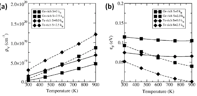
conductivity in c-GeTe Edwards et al.45,46 used density functional theory (DFT) calculations
to successively study the effect of Ge and Te vacancies in Ge-rich and Ge-poor conditions,
all at a variety of temperatures. Computing a perfect vacancy free structure, where the
Fermi level is found near mid-gap, the Ge vacancy formation energy ΔEfGe is negative while
ΔEfTe is positive and on the order of >1eV45. The formation of Ge vacancies in this state
pulls the Fermi energy toward the valance band until the point at which vacancy formation is
no longer energetically favorable. This occurs when the Fermi level is near or even inside
the valence band46, which explains the observation of metallic-like conductivity. Kolobov et
al.47 showed that Ge vacancies lead to restructuring in the local atomic arrangement such that
three Te atoms are left with lone pair electrons for each Ge vacancy.
Upon shifting the chemical equilibrium to a Te-rich state—recall from Section 1.1.2.1 that
“stoichiometric” GeTe can have a range of Ge:Te ratios around 1:1—was found to further
reduce the Fermi level and increase the vacancy concentration (Figure 1.13). Increasing the
temperature from 300-900K, as is the case for all semiconductors, drives the stabilization of
an even higher carrier concentration and (in the case of GeTe) a reduction in the Fermi
energy46. Huang et al. ascribed the low vacancy formation energy to a restructuring of bonds
of the group of balancing driving forces which stabilize the resonantly bonded,
hyper-coordinated, rhombohedrally distorted GeTe crystal structure.
Figure 1.13. (a) Germanium vacancy concentration and (b) Fermi level as a function of
temperature for Ge-rich and Te-rich conditions.46
Departing from the picture of modeled defective GeTe, it has been found that macroscopic
features inherent in the GeTe microstructure can significantly affect carrier concentration and
transport properties. For example, deposition method10,26,38,49, substrate temperature38 and
thickness38,50 have all been shown to strongly affect GeTe resistivity. Furthermore Ge:Te
ratio49,51 and dopants/alloying elements5,27,52 also affect GeTe resistivity. Transport
properties for GeTe in general are highly variable based on literature values—room
temperature mobility tends to be in the range of 5-100cm2/V-s and carrier concentration
temperature dependence of mobility and carrier concentration for various deposition
temperatures is shown in Figure 1.14. Note these samples were sputtered on glass substrates.
On the whole, it is interesting to note that irrespective of deposition method, substrate
temperature, annealing time, annealing temperature and to an extent composition, c-GeTe
retains a quite substantial electrical conductivity. Compared to most metals the conductivity
is not particularly impressive but compared to other semiconductors—of which GeTe is
one—GeTe appears unmatched in its conductivity. Furthermore, the microstructural
structural quality observed when attaining this high conductivity is nothing compared to the
perfection required for other commonly used semiconductors, e.g. Si, GaAs and GaN. That
is, GeTe can sustain substantial structural distortion and defectivity without sacrificing
conductivity, likely due entirely to the quite high carrier concentration. Ultimately this is one
of the primary reasons why GeTe and other PCMs have been so readily implemented in a
variety of technologically viable microelectronics applications. Furthermore, by not
requiring expensive high temperature epitaxial growth processes for a device active layer, a
range of new low cost applications are possible. This will be discussed in greater detail in
Figure 1.14. Transport properties of GeTe as a function of temperature for various
deposition temperatures.38
Moving on to the amorphous phase, the electronic properties of a-GeTe are quite different
from c-GeTe, as is to be expected from the structural discussion in Section 1.1.2.1. In fact,
the connection between structural features of a-GeTe and the resultant electronic properties
has been a focus of intense investigation9,19,23–25,30,31,53–57. In the amorphous state GeTe is
substantial amount of lattice disorder, a substantial reduction in vacancy content, and a
widening of the band gap as compared to c-GeTe by roughly 5%58,59. The loss of
conductivity is explained by the fact that, in contrast to the crystalline phase, the Fermi level
in a-GeTe remains firmly pinned in the midgap state1. In addition to the loss of long range
order, the a-GeTe structure is known to consist of a combination of octahedral and
tetrahedral fragments54,57, the latter of which contain Ge-Ge homopolar bonds25.
Interestingly, homopolar bonds are also observed in the liquid phase and become trapped in
the solid phase upon cooling25. Extensive disorder notwithstanding, the fact that a-GeTe
retains many structural fragments consistent with the crystalline phase is actually one
explanation for the capability of fast switching between amorphous and crystalline states.
That is, existing octahedral fragments can seed nucleation and growth processes,
Figure 1.15. Normalized cell resistance and threshold voltage (Vth) as a function of time for
an a-PCM.53
One other interesting, and possibly troublesome, electronic property of a-GeTe is the
observed increase in resistivity and threshold voltage as a function of time following the
melt-quench process53. As seen in Figure 1.15, the increase in each can be quite dramatic
over a relatively short timeframe. Since this property is detrimental to the PCM-based digital
memory community, methods to understand and ultimately manage it have received much
attention from the research community1,9,25,53,59. The most compelling explanation to date
changes in the bonding environment to electronic features such as band gap, resistance drift
coefficient, an Fermi energy9. Ultimately the authors found that, while the initial structure of
as-quenched GeTe contains Ge-Ge homopolar bonds and related tetrahedral fragments, the
global structure transitions to 6-fold coordination seen in c-GeTe and a loss of various defect
states are observed. In spite of the fact that the structure is relaxing toward the stable
c-GeTe, the magnitude of the Peierls distortion observed in relaxed a-GeTe is substantially
higher than that of c-GeTe. Hence, while a Peierls distortion is observed in many resonantly
bonded materials, it is actually a destructive feature for resonance, and taken to a more
complete extent it completely diminishes electronic features associated with resonant
bonding.
Having summarized the primary electronic characteristics for a-GeTe and c-GeTe it is clear
that the electrical properties of any device based on this material will critically depend on
both macroscopic and microscopic features. Therefore, on the one hand improving GeTe
thin film morphology can serve to improve device characteristics, and on the other hand
having an understanding of the connection between microstructure and electronic properties
will allow one to diagnose changes or degradations in device performance in the context of
micromorphology. It is these two points that form the primary motivation for this body of
work—that is developing and understanding how GeTe morphology can improve the
1.1.3
The Phase Change Process
The previous sections have discussed structural, optical and electronic characteristics of
a-PCMs and c-a-PCMs, and specifically how local order (or a lack thereof) and bonding motifs
control observed properties. The following section discusses the various mechanisms by
which PCMs are converted between these states, factors that control the switching process
and other important elements of the phase change.
At the most basic level, to amorphize any material it must be given enough energy to drive
randomization at the atomic level, followed by removal of that energy at such a rapid rate
that the atoms are not able to relax to a more energetically favorable—that is, ordered—state.
The amorphous state is a metastable one for many materials, a state only sustained by the
kinetic limitations of low atomic mobility. Amorphization is commonly achieved by using
thermal energy to heat a material above its melting point, followed by rapidly introducing the
material to a cold medium. To demonstrate this same process on a microscale, i.e. for thin
films, energy pulses of various types must be used. This is predominantly a thermal process,
although the source of thermal energy may have its origins in an optical or electrical source,
which is to say photon absorption or joule heating. The energy pulse must be large in
amplitude, short in duration and sufficiently localized. Furthermore the local environment of
the material must be able to rapidly move thermal energy into a larger thermal reservoir such
that the equalized temperature is low. Finally, the material itself must be conducive to
state is sustained. If any of these conditions are not met, the amorphous state will not be
achievable.
Taken again from a basic level, the process of crystallization can occur as a solid-solid
transformation (i.e. upon heating) or a liquid-solid transformation (i.e. upon cooling). In
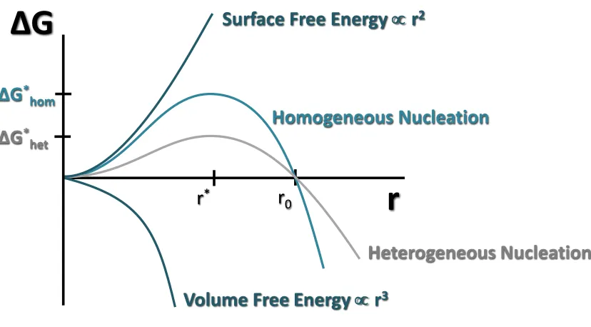
either case the driving force for nucleation in a classical sense is a balance between the
decrease in volume free energy, increase in surface free energy and increase in misfit strain
energy. This relationship is depicted schematically in Figure 1.16 as a function of nuclei
radius. Homogeneous nucleation is the process which occurs in an interface-free medium,
whereas heterogeneous nucleation involves the utilization of high energy surfaces (e.g. high
angle grain boundaries) as nucleation sites. In this case the surface energy term is a balance
between increased surface energy from the nuclei and decreased surface energy originating
from the destruction of preexisting surfaces. For both nucleation processes, the initial
increase in radius causes an increase in free energy, proportional to r2, as the surface
area-to-volume ratio is high and the surface energy term is large. At some point the nuclei will reach
a critical radius r*, beyond which the decrease in volume free energy, proportional to r3, fully
stabilizes the nucleation and growth process. In the case of heterogeneous nucleation the
required energy barrier is reduced significantly by differential surface energy reductions, but
Figure 1.16. Classical nucleation scheme showing Gibbs free energy as a function of nuclei
radius comparing homogeneous and heterogeneous nucleation processes. Curves expressing
surface and volume free energy terms are included for reference.
Moving now to the specific case of PCMs, since they are typically implemented as thin films
in a multilayer device stack the opportunity for heterogeneous nucleation is always present.
However, it has been found that the tendency for growth dominated crystallization (i.e. low
bulk nucleation rate) or nucleation dominated crystallization (i.e. high bulk nucleation rate) is
highly dependent on PCM composition and local environment61–66. A thorough discussion of
this topic can be found in Section 4.2. Beyond initial nucleation processes, the dynamics of
crystallization can be understood in the time-temperature-transformation (TTT) landscape,
where crystallization must be viewed as a balance between the driving force for nucleation
ΔG
r
r
0ΔG
* homΔG
* hetHomogeneous Nucleation
Heterogeneous Nucleation
Surface Free Energy
∝
r
2Volume Free Energy
∝
r
3retention time—i.e. the speed with which a metastable a-PCM spontaneously crystallizes as a
function of temperature—and maximum quench time allowed to achieve the a-PCM state.
Figure 1.17. Generalized PCM time-temperature-transformation (TTT) diagram (left) atomic
mobility (center) and driving force for crystallization (right) as a function of temperature.1
From Figure 1.17 it is clear that stabilizing the amorphous phase for PCMs can be a difficult
process, given the required quenching speed. The tendency of a liquid to be quenched into a
glassy state is identified with a measure of liquid “strength” or “fragility”. By plotting
viscosity as a function of inverse temperature normalized to the glass transition temperature
Figure 1.18. Viscosity as a function of reciprocal temperature normalized to the glass
transition temperature (Tg) for a variety of materials.67
Around the glass transition temperature atomic mobility (inverse viscosity) is by definition
very low; however, for PCMs very slight positive deviations in temperature facilitate a sharp
increase in atomic mobility. This can be seen in Figure 1.19, where growth velocity peaks
Figure 1.19.Crystal growth velocity of GeTe as a function of temperature, measured directly
via transmission electron microscopy.69
As a point of reference for this discussion, Figure 1.20 shows for a wide variety of materials
the relationship between temperature at which maximum growth rate is observed (Tmax) and
the glass transition temperature (Tg) follows a 1.48:1 ratio within 10%63. This establishes an
upper limit to the margin for amorphization. Of critical importance, PCMs fall within a
normal thermal deviations from room temperature and (2) not so high as to be inaccessible
with reasonably applied thermal energy sources.
Figure 1.20. Relationship between the temperature at which maximum growth rate occurs
(Tmax) and the glass transition temperature (Tg) for various materials. The Tmax/Tg ratio is
consistently 1.48±0.15 for all studied materials.63
Of course the preceding discussion has important implications for device structure
Having an understanding of fundamental PCM properties, the discussion is now extended to
PCM applications.
1.2
Applications of Phase Change Materials
Section 1.1 discussed the nature of amorphous and crystalline PCMs, as well as the diversity
of their resultant physical properties. The following sections will summarize how these
properties were harnessed to create platforms for optical storage, digital memory and
electronic switch technologies.
1.2.1
Optical Storage
Applications involving the optical properties of PCMs are mentioned here only briefly, as
they are an important part of the PCM development timeline but are somewhat tangential to
the present body of work. Yamada et al.32 successfully demonstrated that (GeTe)x(Sb2Te3)1-x
alloys in an optical disc configuration could be successfully cycled between the amorphous
and crystalline state using ns-scale laser pulses. The authors found an energy landscape in
which laser pulse amplitude and duration were varied to stabilize both the melt-quenched
amorphous and crystallized phases. Relying on the previously described optical contrast
attainable with PCMs, this became a cost-effective, scalable technology for rewritable optical
storage media. As the thin film structure and PCM material properties were optimized,
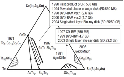
storage capability and write speed were dramatically increased7. Figure 1.21 shows relevant
Figure 1.21. Schematic ternary diagram identifying important PCM compounds and related
optical storage media technology nodes.7
1.2.2
Non-Volatile Digital Memory
As early as 1968, phase change materials were observed to have an electrically switchable
“memory effect”, where high and low resistance states could be repeatedly attained2. In the
subsequent decades an entire industry was built around this concept, now called “storage
class memory”, which represents a much faster and non-volatile storage option compared to
Figure 1.22. (a) Schematic of a PCM memory cell. Fabricated cell in the (b)
ON/SET/crystalline state and (c) OFF/RESET/amorphous state.70
To achieve high storage densities required by modern computing technologies, multilevel
arrays based on the PCM “mushroom cell” (Figure 1.22) have been developed. In this
structure a PCM is sandwiched between a top and bottom electrode and surrounded by an
insulator. These devices are self-switching in nature, where the OFF state is achieved by
passing a current directly through the PCM, joule heating induces melting and rapid removal
of thermal energy establishes a quenched amorphous state. The ON state is achieved by
establishing an electric field between top and bottom contacts, the magnitude of which is
large enough to create a small crystalline filament that draws enough current to heat the local
environment above the crystallization temperature. Lastly, a much lower amplitude voltage
READ pulse is applied to assess the resistance state of the device. The temporal nature and
relative amplitude of each pulse are shown schematically in Figure 1.23.
Figure 1.23. Schematic showing voltage pulse magnitudes and durations to required achieve
“SET” and “RESET” states, as well as “READ” voltage. After ref70.
Critical aspects of PCM-based NVM include OFF-state retention time, crystallization
temperature, crystallization speed, threshold voltage and melting temperature. At an even
more basic level, the memory cell architecture and chosen materials must remain stable when
exposed to high temperature excursions and potentially reactive materials. OFF-state
retention for phase change memory is related to the stability of the PCM amorphous state as a
function of temperature and time. Since the “RESET” state is a critical part of the binary
memory cell operation, any change to the measured properties of this state will negatively
affect device performance. This can include the upward resistance drift discussed in Section
1.1.2.4 or a reduction in cell resistance due to full or partial recrystallization of the
amorphous state. The complete loss of cell data associated with the latter point prompted the
critical design specification of a minimum 10 year state retention at 80°C 70. Fortunately
Voltage
Time
T
cryst
T
melt
RESET
SET
there are many materials which can match this criterion while also fulfilling other
specifications. A relatively straightforward way to predict OFF-state retention in a memory
cell is to measure the crystallization temperature (Tcryst) of blanket PCM films.
Figure 1.24. Variation in electrical resistance with temperature for GeTe showing the
transition from the amorphous (resistive) to crystalline (metallic) state. Data from71, model
from60.
As is shown in Figure 1.24 for GeTe, measuring the resistance of the initially amorphous
PCM as a function of temperature one can observe the abrupt drop in resistance which occurs
0
50
100
150
200
250
R
es
is
ta
n
ce (
Ω
)
Temperature (
oC)
when the PCM crystallizes. This method has its limitations, however, since it represents the
composite effects of nucleation and growth processes, is sensitive to temperature ramp rate
and because it has been shown that as-deposited amorphous PCMs crystallize very
differently than melt-quenched PCMs72. As such, crystallization is often evaluated using
various types of Kissinger analyses67 which account for crystallization kinetics by
incorporating heating rate and ultimately provide a composite crystallization activation
energy. Since this method also does not distinguish between nucleation and growth
processes electron microscopy methods can be used to directly visualize the transformation
process50,65,69,73–76. From these analyses it can be seen that PCMs of different compositions
often crystallize in vastly different fashions; that is, growth velocity, nucleation activation
energy and crystallization temperature all depend on composition, structural history of the
PCM and surrounding device architecture55,60,61,63,64,77–83. Given the wide range of observed
crystallization behaviors and associated OFF state retention capabilities, proper PCM
selection is extremely important.
In an extension of relevant OFF state properties and crystallization mechanics, NVM cells
rely on a phenomenon called threshold switching to convert from the amorphous to
crystalline state. Threshold switching is a moniker derived from the concept that a voltage
applied to an OFF state PCM cell, above a certain threshold, will cause spontaneous state
conversion. Microscopically, this process is understood to consist of voltage induced
formation of crystalline filaments within the amorphous matrix which are needle-like in