ABSTRACT
TAN, KAI. Development of Solid State Circuit Breakers for 380V DC Microgrid Protection. (Under the direction of Dr. Alex Q. Huang and Dr. Iqbal Husain).
Development of Solid State Circuit Breakers for 380V DC Microgrid Protection
by Kai Tan
A dissertation submitted to the Graduate Faculty of North Carolina State University
in partial fulfillment of the requirements for the degree of
Doctor of Philosophy
Electrical Engineering
Raleigh, North Carolina 2017
APPROVED BY:
_______________________________ _______________________________ Dr. Alex Q. Huang Dr. Iqbal Husain
BIOGRAPHY
The author, Kai Tan was born in Lanzhou, Gansu, P.R. China and received a Bachelor degree in Electrical Engineering from the Department of Electrical Engineering, Tsinghua University, Beijing, P. R. China in 2007.
ACKNOWLEDGMENTS
First and foremost, I would like to thank my advisor Professor Alex Qin Huang for his guidance, encouragement, and support during the past six years. His broad knowledge and insightful understanding of power electronics have helped me enormously.
The help from faculties and staffs in the FREEDM system center are appreciated. I would especially thank my committee members, Professor Iqbal Husain, Professor Srdjan Lukic, and Professor David Lubkeman, who have given me lots of useful suggestions to improve the quality of this dissertation. Thanks, Professor Xiangwu Zhang from College of Textiles for serving as the graduate representative in my Ph.D. committee.
I am also very grateful to my fellow students with whom I have worked together in FREEDM system center in last 6 years. I’d like to thank Dr. Xiaohu Zhou, Dr. Jun Li, Dr. Qian Chen, Dr. Gangyao Wang, Dr. Zhigang Liang, Dr. Yu Du, Dr. Pochih Lin, Dr. Zhengping Xi, Dr. Sanzhong Bai, Dr. Zhan Shen, Dr. Xu She, Dr. Xunwei Yu, Dr. Edward Van Brunt, Dr. Sumit Dutta, Yalin Wang, Dr. Yen-mo Chen, Dr. Xing Huang, Huan Hu, Li Jiang, Xingchen Yang, Dr. Xiang Lu, Dr. Arun Kadavaelugu, Dr. Dany Fregosi, Ryan Meitl, Philip Funderburk, Dr. Mengqi Wang, Dr. Wencong Su, Dr. Gahzal Falahi, Dr. Rui Wang, Dr. Fei Wang, Dr. Meng-chia Lee, Dr. Xiaomin Li, Dr. Ankan De, Dr. Elie Najm, Dr. Mohammad Ali Rezaei, Rui Gao, Suxuan Guo, Yang Lei, Yizhe Xu, Dr. Changjian Hu, Dr. Xiaoqing Song, Fei Xue, Dr. Chang Peng, Qi Tian, Dr. Xijun Ni, Dr. Xiaofeng Yang, Dr. Dong Chen, Dr. Wenxi Yao, Dr. Wu Chen, Dr. Qiwei Lu, Yang Xu, Haotao Ke, Qingyun Huang, Zhiping Chen, Qianglai Zhu, Liqi Zhang, Pengkun Liu, Siyuan Chen, Zheyuan Cheng and many more who are not mentioned here.
TABLE OF CONTENTS
LIST OF TABLES ... VIII LIST OF FIGURES ... IX
CHAPTER 1 INTRODUCTION ... 1
1.1 Research background ... 1
1.2 Review of 380V DC Microgrid Eco System ... 3
1.3 Issues in DC Microgrid Protection and Proposed Solution ... 5
1.3.1 Arcing ... 5
1.3.2 DC Bus Capacitance ... 6
1.3.3 Protection Speed ... 7
1.3.4 Proposed solution ... 9
1.4 Dissertation Outline ... 11
CHAPTER 2 SOLID STATE DEVICES FOR DC CIRCUIT BREAKER APPLICATION 14 2.1 Introduction and Motivation ... 14
2.2 Specific Characteristics for DC Circuit Breaker Application ... 16
2.2.1 Typical Operations Stages of DC Circuit Breaker Application ... 16
2.2.2 Characteristics criteria for circuit breaker application ... 20
2.3 Candidates for 380V DC Microgrid protection ... 23
2.3.1 Characteristics for node solid state circuit breaker ... 24
2.3.2 Characteristics for branch circuit breaker ... 31
2.4 Conclusion and summary ... 39
CHAPTER 3 HOT SWAPPABLE OUTLET FOR 380V DC SYSTEM ... 41
3.1 Introduction and Motivation ... 41
3.2 State of Art DC Outlet ... 43
3.2.1 Saf-D-Grid® plug and receptacle ... 43
3.3.2 Operation Modes Analysis for Hot Swappable Outlet ... 54
3.3.3 High Ratio Buck DC/DC Converter PSU ... 56
3.3.4 Dual Threshold Over Current Protection ... 57
3.3.5 Over Temperature Protection ... 58
3.4 Experimental Results of Hot Swappable Outlet ... 58
3.5 Conclusion and Summary ... 62
CHAPTER 4 SOLID STATE CIRCUIT BREAKER FOR 380V DC SYSTEM ... 65
4.1 Introduction and Motivation ... 65
4.2 State of Art DC Circuit Breaker ... 66
4.2.1 CX-series DC circuit breakers ... 66
4.2.2 Ultrafast autonomous SiC JFET circuit breaker ... 68
4.2.3 400V DC SiC-SIT circuit breaker by NTT Japan ... 70
4.3 Hardware Design and Analysis ... 72
4.3.1 Circuit topology ... 72
4.3.2 Interleaved hiccup start up with inrush current strategy ... 73
4.3.3 Transient and steady state real-time junction temperature monitoring ... 76
4.3.4 High impedance fault protection ... 78
4.4 Experimental Results of Solid State Circuit Breaker ... 79
4.4.1 Hardware design ... 79
4.4.2 Interleaved hiccup start up with inrush current strategy ... 81
4.4.3 Steady state thermal performance ... 84
4.4.4 Dual threshold over current protection ... 87
4.4.5 Transient real-time junction temperature monitoring ... 91
4.5 Conclusion and summary ... 96
CHAPTER 5 HYBRID CIRCUIT BREAKER FOR 380V DC SYSTEM ... 98
5.1 Introduction and Motivation ... 98
5.2 Hardware Design and Analysis ... 99
5.3.1 Feature analysis for DC circuit breaker application ... 101
5.3.2 Mechanism analysis of selected high current relay ... 104
5.3.3 Novel driving strategy with performance enhancement ... 111
5.5 Experimental Test and Verification ... 114
5.5.1 Insulation test and verification ... 114
5.5.2 Driving strategy test and verification ... 116
5.5.3 Transient of current commutation test ... 126
5.6 Conclusion and Summary ... 128
CHAPTER 6 SUMMARY AND FUTURE WORK ... 130
6.1 Summary ... 130
6.2 Future Work ... 133
LIST OF TABLES
Table 2.1 Definitions of MOSFET Parameters... 14
Table 2.2 Characteristics of Solid State Devices for DC Circuit Breaker Application .. 24
Table 2.3 RDS,SP(ON) comparison of 4 candidates... 24
Table 2.4 Thermal impedance of 4 candidates ... 25
Table 2.5 VGS and RG_external values for each device in long pulse test ... 34
Table 2.6 Characteristics of Solid State Devices for Long pulse turn-off test ... 39
LIST OF FIGURES
Figure 1.1 DC micro grid in FREEDM systems center ... 2
Figure 1.2 Summary of 380V DC eco-systems ... 3
Figure 1.3 HP 2U DL380 servers and 4U 980 servers ... 4
Figure 1.4 DC power strips from multiple manufacturers ... 4
Figure 1.5 Snapshots of arc behavior in 400V DC disconnection[21] ... 5
Figure 1.6 DC Voltage endurance envelope proposed by EPRI and IEEE[26] ... 7
Figure 1.7 15A MCCB trip curve[30] ... 8
Figure 1.8 Circuit protection hierarchy for DC data center application ... 9
Figure 2.1 Proposed operation strategy for circuit breaker... 17
Figure 2.2 RDS(ON)-TJ coefficient of 4 candidates for steady state ... 26
Figure 2.3 (a) Short pulse saturation test setup, (b) Typical short pulse test with saturation current ... 27
Figure 2.4 Saturation current vs. Junction temperature ... 28
Figure 2.5 Long pulse saturation current sharing of paralleled Si CoolMOSTM ... 28
Figure 2.6 Long pulse saturation current sharing of paralleled SiC JFET ... 30
Figure 2.7 Multiple pulse saturation current sharing of paralleled SiC JFET ... 31
Figure 2.8 Long Pulse Test Circuit for high current turn-off capability under 400V DC bus ... 32
Figure 2.9 Hardware bench setup for high current saturation turn off test ... 33
Figure 2.10 Switching waveforms of C2M0025120D under RG_external = 2.5Ω and 5Ω . 34 Figure 2.11 Test results of Si MOSFET STY145N65M5 in high current saturation turn off test ... 35
Figure 2.12 Test results of Si MOSFET IPW65R019C7 in high current saturation turn off test ... 36
Figure 3.2 (a) Hardware configuration of FUJITSU® DC Outlet (b) Specifications of
FUJITSU® DC Outlet ... 46
Figure 3.3 (a) Characteristic of PPTC materials and circuit scheme (b) Comparison of test under 550V / 20A DC ... 48
Figure 3.4 (a) Circuit topology of DC outlet (b) Proposed control scheme ... 49
Figure 3.5 (a) DC hot swappable outlet (b) Hardware of outlet ... 50
Figure 3.6 Topology and state (a) & state (b) of designed hot swappable outlet with connected 380/48 V DC/DC load (c) Hardware configuration of embedded hot swappable outlet circuit ... 53
Figure 3.7 Operation modes of proposed outlet... 54
Figure 3.8 Buck converter for supply drive power ... 56
Figure 3.9 Dual thresholds off strategy for over current trip ... 57
Figure 3.10 Hot pluggable outlet hardware ... 58
Figure 3.11 Plug in process waveforms of DC hot pluggable outlet ... 59
Figure 3.12 Hiccup startup process waveforms of DC hot pluggable outlet ... 59
Figure 3.13 Normally on Steady state thermal image ... 60
Figure 3.14 Unplug process waveforms of DC hot pluggable outlet ... 60
Figure 3.15 Lower threshold with timer over current protection waveforms of DC hot pluggable outlet ... 61
Figure 3.16 instantaneous over current protection waveforms of DC hot pluggable outlet ... 61
Figure 3.17 Over temperature protection waveforms of DC hot pluggable outlet ... 62
Figure 4.1 (a) Hardware configuration of CX-series DC circuit breaker (b) Trip time curve of CX-series DC circuit breaker ... 66
Figure 4.2 (a) Hardware of Autonomous SiC JFET circuit breaker (b) Circuit schematic configuration (c) Short circuit waveforms of self-powered SiC JFET SSCB ... 68
Figure 4.3 (a) Hardware of SiC-SIT NTT DC circuit breaker (b) Circuit schematic configuration (c) Experimental waveforms comparison of original and proposed gate voltage ... 70
Figure 4.4 Circuit topology of proposed solid state circuit breaker ... 72
Figure 4.8 RDS(ON) vs. junction temperature ... 78
Figure 4.9 Hardware of solid state circuit breaker (140 mm × 110 mm × 40 mm) ... 80
Figure 4.10 Interleaved hiccup close loop startup waveform for 190V/100uF/10A ... 82
Figure 4.11 Zoom in multi-channel close loop constant ID control waveform ... 83
Figure 4.12 Cooldown interval of each group ... 84
Figure 4.13 Hard configuration of steady state thermal test ... 84
Figure 4.14 Thermal image of heatsink surface view in steady state ... 85
Figure 4.15 Thermal image of side view in steady state ... 86
Figure 4.16 Lower threshold OCP with 32A threshold and 800us timer ... 87
Figure 4.17 Adaptive gate voltage of Si MOSFET as instance ... 88
Figure 4.18 Zoom in waveform of programmed adaptive gate voltage in low threshold OCP ... 89
Figure 4.19 High threshold OCP with saturation current close loop control... 90
Figure 4.20 Adaptive gate voltage for saturation current control in high threshold OCP ... 90
Figure 4.21 Short pulse test with 7.5A ID and different TJ and VDS ... 92
Figure 4.22 Data points from short pulse test for 7.5A and 3D curve fitting result ... 92
Figure 4.23 3D surface data linear polyfit curve fitting... 93
Figure 4.24 VGS and VDS of first saturation pulse ... 94
Figure 4.25 Result of transient junction temperature monitoring ... 94
Figure 4.26 (a) Transient thermal impedance of tested device (b) Pulse length of first saturation pulse ... 95
Figure 5.1 Circuit topology of hybrid branch circuit breaker ... 99
Figure 5.2 Control strategy of hybrid branch circuit breaker ... 101
Figure 5.3 Picture of high current mechanical relay ... 103
Figure 5.4 Hardware configuration of high current mechanical relay ... 105
Figure 5.10 Force analysis of ON to OFF... 111
Figure 5.11 official recommended drive waveform and proposed drive waveform ... 111
Figure 5.12 Proposed driving scheme to reduce contact resistance ... 112
Figure 5.13 Force analysis of ON state with proposed Von ... 113
Figure 5.14 Steady state insulation test setup ... 114
Figure 5.15 Steady state insulation test voltage drop waveforms ... 115
Figure 5.16 test circuit for proposed driving strategy ... 117
Figure 5.17 Typical turn off transient waveform ... 117
Figure 5.18 Pulse voltage on reset coil ... 118
Figure 5.19 The current waveforms on reset coil for 12V to 60.1V ... 119
Figure 5.20 The current waveforms on diode for 12V to 60.1V ... 120
Figure 5.21 The voltage drop on relay for 12V to 60.1V ... 121
Figure 5.22 Hardware of hybrid branch circuit breaker ... 121
Figure 5.23 Minimized current commutation loop in PCB design ... 122
Figure 5.24 The delay of turn off for 30V and 50V ... 123
Figure 5.25 The turn off test for 200A and 50V driving voltage ... 124
Figure 5.26 Zoom in waveform for 200A and 50V driving voltage ... 125
Figure 5.27 Conducting resistance on Mechanical relay without driving voltage and with 5V driving voltage ... 126
Figure 5.28 Phenomenon of pre-commutation ... 127
Figure 5.29 Transient process of current commutation ... 128
C
HAPTER
1
Introduction
1.1 Research background
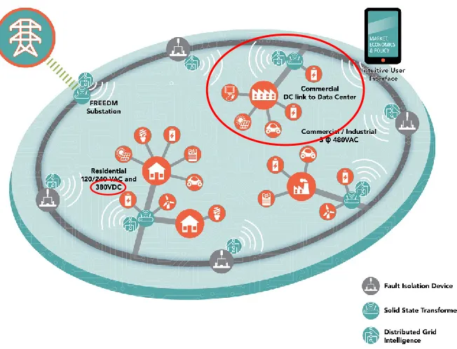
Figure 1.1 shows the DC microgrid in the plan of Future Renewable Electric Energy Delivery and Management System[1]. The DC microgrid system is a port with bi-directional power flow capability and high efficiency since the skip of low voltage DC/AC inverter which is the lowest efficient part in SST. [2]
Besides DC microgrid in FREEDM system, the DC distribution system has also been investigated in DC shipboard, airplane system, telecommunication system, DC buildings, and DC data centers, etc. [3]–[15]
1.2 Review of 380V DC Microgrid Eco-System
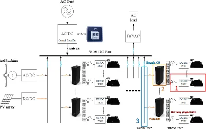
For 380V DC system, the eco-system[16] from chip to the grid is being built and developed by many manufacturers. Figure 1.2 shows a brief summary of 8 kinds of equipment. The DC circuit breaker, power distribution strip, connector and ICT load are the equipment our research most interested in.
In Zurich, Switzerland, May 30, 2012, ABB and Green® launched 380V DC data center employing HP servers with ±190V DC bus. HP provided the HVDC-enabled IT for this technology showcase, including servers and storage, such as HP X1800 G2 Network Storage
The power rating is about 2A for DL380 2U and 3.5A for DL980 4U. Figure 1.4 shows how the servers connected with power strips [16]. Each server is plugged into one socket. About 4 sockets are protected with a circuit breaker or fuse.
Figure 1.3 HP 2U DL380 servers and 4U 980 servers
HP ProLiant DL980 G7 Server (4U)
For your largest and most demanding enterprise-class workloads 1400W kit
HP ProLiant DL380 G9 Server (2U)
Compute and storage ideal for essential data center needs 800W power kit *2 (G7 is 750W*2,consider the redundancy)
1.3 Issues in DC Microgrid Protection and Proposed Solution
Although there are many benefits for applying DC distribution system in above applications. There are several issues in DC system protection which are not critical in AC system. Those issues slow down the speed of DC distribution system development in industry.
1.3.1 Arcing
1.3.2 DC Bus Capacitance
The second important issue is the large capacitance connected to the DC bus. It helps to keep the DC voltage stiff with small ripple and filter the high-frequency harmonics to decouple the power with limited line inductance. However, the inrush current may cause unexpected circuit breaker trip when the user’s capacitance is connected to the DC grid and bus. And the
1.3.3 Protection Speed
Another important aspect is the trip speed of circuit breaker. Figure 1.7 gives the trip curve of a 15A MCCB[27], [28]. The trip speed of 15A MCCB is slow (10~100ms) with a high
All other PSU will also be affected because the long trip time has already exceeded the low voltage ride through capability of PSU. The DC bus voltage will drop to a low value and affect the whole neighborhood. For avoiding this low voltage, all PSU nearby need to have larger capacitance for stronger low voltage ride through capability which deteriorates the second aspect above. In sum, the slow trip speed of traditional mechanical circuit breaker requires larger bus capacitors to meet hold up time requirement for slow fault clear speed.
1.3.4 Proposed solution
Considering all above aspects, a 380V DC system protection architecture is proposed with 3-level hierarchy circuit protection architecture[29]. A DC datacenter application with unidirectional power flow is employed to demonstrate the protection system in Figure 1.8.
1) PSU level 1
Each 2U or 4U server of the data center is connected with a hot-swappable solid state outlet. It has basic overcurrent protection and current limiting capability with the fastest speed to trip the downstream fault in zone 1 without impacting other servers in the neighborhood. The inrush startup capability is designed for capacitive 0-380V startup. More importantly, the outlet extinguishes the arcing with embedded solid state devices makes the plug and unplug similar to traditional AC distribution outlet. The nominal current rating is designed at 5A and 2kW for typical 2U or 4U server PSU unit.
2) Nodes level 2
3) Branch level 3
Finally, a hybrid branch circuit breaker is proposed and designed for large current application and multiple nodes. It is a combination of a fast-mechanical switch and solid-state devices to trip high current (180~200A) without arcing and conduct with low loss. The trip speed is slower than solid state device but faster than other traditional mechanical solutions to limit the discharge current and isolate the fault within the branch as in zone 3. Each branch is isolated with hybrid branch circuit breaker without affecting others.
All three levels proposed have current limiting and tripping with fast speed and arcing free, makes the whole system can have stronger low voltage ride through capability with smaller capacitance.
1.4 Dissertation Outline
In Chapter 3, a hot-swappable outlet is developed with the innovative scheme with energizing pad to have zero standby power feature. It also helps to avoid the arcing at the time of disconnection. The operation modes are presented with inrush current limiting, dual threshold overcurrent protection and over temperature protection to enhance its safety and reliability. Experimental results are displayed to verify the implementation of all proposed features.
In Chapter 4, the node solid state circuit breaker is proposed and developed. Multi-channel interleaved hiccup startup and dual threshold overcurrent protection are invented and realized with innovated analog driver circuit close loop control. It helps to trip the fault and saturate the current without influencing other nodes in the neighborhood which can reduce the capacitance in all nodes and redefine the voltage endurance envelope without voltage outrage during node fault. This development helps strengthen the robust of DC microgrid and reduce the cost of capacitors and loss on voltage outrage.
C
HAPTER
2
Solid State Devices for DC Circuit Breaker
Application
2.1 Introduction and Motivation
In this Chapter, multiple solid-state devices are analyzed and evaluated particularly for 380V DC circuit breaker application. As we known, the characteristics and parameters of solid state devices vary at different static and dynamic conditions. Table 2.1 shows part of common definitions of the majority characteristics of a MOSFET as an example.
Table 2.1 Definitions of MOSFET Parameters
Symbol Description
V(BR)DSS Drain-source breakdown voltage
VGS(th) Gate threshold voltage
RDS(on) Static drain-source on-resistance
Qg Total gate charge
Tj Max. operating junction temperature
Most of them are related and determined by the principle of semiconductor physics & devices. These factors affect each other and make the device selection optimization for each hardware design is required.
In traditional switching application, one important method for evaluating MOSFETs is according to Figure of Merit (FOM). It compares the gate charge (Qg) against the static on-state resistance (RDS(ON)).
FOM = 𝑄𝑔× 𝑅𝐷𝑆(𝑂𝑁) (2.1)
In semiconductor devices, the lower the RDS(ON) the higher the Qg will be. So, this multiplication can be used to have a like-for-like comparison and evaluate certain device technologies.
Some other similar methods for comparing devices were also proposed. The “Baliga
However, the concerns for DC solid state circuit breaker is different with previous FOM consideration. Besides, the new SiC devices introduce some new advantage and good features compare with Si devices. It also needs to be considered with foresight. All three circuit breakers have different requirement because of the hardware design and feature differences which is also need to be considered.
In sum, a new method for analysis, evaluation, and optimization in device selection is proposed and defined based on multiple Si and SiC devices. The different criteria for devices between pure solid state and hybrid circuit breaker application are also presented in this chapter.
2.2 Specific Characteristics for DC Circuit Breaker Application
2.2.1 Typical Operations Stages of DC Circuit Breaker Application
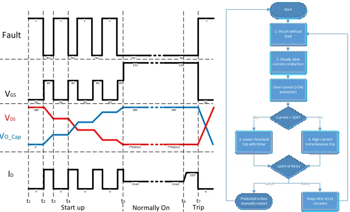
The proposed operation modes and flowchart is shown in figure 2.1. It can be identified as latch off mode, inrush hiccup startup mode, normally on mode, dual threshold over current trip and over temperature trip.
A. Latching off mode:
Before t2 and after t7, the whole circuit breaker is latched off. The devices are controlled in open circuit to trip the main circuit due to over current or over temperature fault. The fault indicator is high to indicate a fault condition.
0V 380 0V 12V 8V 0V 8V 0V 8V 0V 8V VDS VGS
Start up Trip
1
VO_Cap
0 I*Rds(on)
380
0 0 0 0
Fault
ID
I load I load I*Rds(on) 380
12V
0
Normally On
t1 t2 t3 t4 t5 t6 t7
OCP No
1 1 1
No No No
1
No
Figure 2.1 Proposed operation strategy for circuit breaker Start
1. Inrush without load
2. Steady state current conduction
Over current (>5A) protection
Current > 10A?
3. Lower threshold trip with timer
4. High current instantaneous trip
Latch or Retry
Keep retry try to recovery Protected unless
manually restart
No Yes
B. Hiccup startup mode:
At the moment of t2, the circuit breaker is set up to start manually or remotely with fault been cleared. The sum of the drain to source voltage on devices of two bus is equaled to 380V because the output bus capacitor voltage is zero. The devices are still in off state with only leakage current. From t2, the control circuit initializes the designed hiccup startup and generates a low VGS close to threshold VT to ensure the devices works in the saturation region to limit the current with a short pulse (t2-t3). The output capacitor is charged a train of pulses like this and its voltage is increased. The drain to source voltage on devices is still large which makes power stress large during the pulse because it operates in saturation. Therefore, the pulse width and the value of limited current need to be designed within the safe operation area (SOA) of the N channel MOSFET device to avoid the device failure due to the excessive power dissipation. After each short pulse, the device is off again from t3-t4 to control the average power stress and cool the device down. The voltage on the device and capacitor remain the same during this period.
C. Normally on mode:
The solid-state circuit breaker works in normal conduction mode. The devices keep fully turn on to keep lowest RDS(ON) so the power loss on the solid-state device is minimized.
D. Overcurrent trip:
The strategy is implemented by a controller to monitor over current or short fault. The current threshold ILimit is used to trip the real over current fault and filter nuisance transient noises.
E. Over temperature trip:
2.2.2 Characteristics criteria for circuit breaker application
One of the most crucial components in DC solid state circuit breaker is the embedded solid-state device. Traditionally, Si devices including MOSFET, IGBT and etc. are considered the best options among all solid state devices in low voltage range[35]–[37]. And a lot of researchers proposed and developed many new designs based on SiC devices due to the development of power devices technology in recent years[32], [38]. For developing the proposed 380V/15A solid state circuit breaker using paralleled devices, the criteria for choosing the solid-state device in proposed design is discussed[39]. From the analysis in the previous section, the most important characteristics of solid state device for 380V DC circuit breaker application are listed:
1. Static conduction resistance (RDS(ON)):
2. Thermal impedance in steady state and transient state:
The steady state thermal resistance can be calculated with:
𝑅𝑡ℎ= 𝐿
𝑘𝐴 (2.2)
L is the thickness of the material (cm), A is the area of the material (cm-2), and k is the thermal conductivity (W∙cm-1∙K-1).
For the SiC, this value is about 4.9 and Si is about 1.5 [40], [41]. This makes the steady state thermal resistance of SiC device much better than Si device with same L and A. It also means that the die size of SiC device can be saved to achieve equivalent thermal resistance with larger die size Si device.
For the same heatsink design and power loss, the device junction temperature will be lower if the steady-state thermal resistance is smaller. It means that the smaller steady-state thermal resistance can work with more compact heatsink design to save the cost.
3. Temperature coefficient in the steady and transient state:
The steady state temperature coefficient is important to achieve evenly current sharing for paralleled operation. The MOSFET device is better than IGBT on this characteristic makes it can be easily used for multiple MOSFET parallel operation to share the large steady-state current and thermal stress.
For the hiccup startup, the saturation current is a function of the drain to source voltage, the gate voltage, and junction temperature:
𝐼𝐷 = 𝑓(𝑇𝐽, 𝑉𝐺𝑆, 𝑉𝐷𝑆) (2.3)
The paralleled devices have same VDS and VGS. However, the threshold voltage VT of devices varies in ±1V makes the initial ID on each device are not equal. The larger saturation ID brings larger thermal stress and higher junction temperature with self-heating.
𝑃1 = 𝐼𝐷1∙ 𝑉𝐷𝑆 > 𝐼𝐷2∙ 𝑉𝐷𝑆 = 𝑃2 (2.4)
4. Temperature range:
The SiC devices can work with much higher junction temperature than Si device, which makes SiC devices have more margin for hiccup startup, over current and over temperature trip and lower risk in failure due to the high junction temperature.
5. Drive circuit power consumption:
The power consumption of driver circuit is a part of total power loss besides the device conduction loss. The normally ON feature of SiC JFET from USCi makes it can consume the least power on driver circuit with 0V VGS. The current driven BJT will consume more power in driver circuit compare with voltage driven MOSFET.
2.3 Candidates for 380V DC Microgrid protection
2.3.1 Characteristics for node solid state circuit breaker
Characteristics and Specifications Analysis and comparison:
1. Static conduction resistance (RDS(ON)):
As stated above in section III, the RDS(ON) can be evaluated with considering its die size, the specified value is listed in table 2.3.
From Table.3 2, the SiC JFET is the best candidate considering the die size. Value of SiC devices is 1/3 to 1/4 of Si devices. This makes SiC devices very competitive in circuit breaker application with smaller die size and lower power loss compare with Si devices.
Table 2.2 Characteristics of Solid State Devices for DC Circuit Breaker Application
Type Manufacturer Part No. V(BR)DSS
(V) @25 °C(mΩ)RDS(on) Die Size (mm2)
Si MOSFET Infineon IPW65R019C7 650 19 68.29
Si MOSFET ST STY145N65M5 650 14 121.88
SiC MOSFET WOLFSPEED C2M0025120D 1200 25 26.02
SiC JFET USCi UJN1205K 1200 45 9.42
Table 2.3 RDS,SP(ON) comparison of 4 candidates
Type Manufacturer Part No. @25 °C(mΩ)RDS(on) Die Size (Cm2) Rds,SP(ON)@25
°C(mΩ*cm2)
Si MOSFET Infineon IPW65R019C7 19 0.6829 12.9751
Si MOSFET ST STY145N65M5 14 1.2188 17.0632
SiC MOSFET WOLFSPEED C2M0025120D 25 0.2602 6.505
2. Thermal impedance in steady and transient state
The typical steady-state thermal resistance is listed in table 3. And specified value is calculated with die size.
The calculated results are close to previous analysis in section 2.2. The SiC devices have larger thermal conductivity makes its thermal resistance is about 1/3 to 1/4 of Si devices with same die size or SiC devices can have similar thermal resistance with 1/3 to 1/4 die size compared with Si devices.
3. Temperature coefficient in steady and transient state
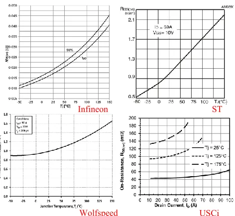
The all four candidates have positive RDS(ON) -TJ coefficient which is good for steady state current sharing with the paralleled operation. It is shown in Figure 2.2.
Table 2.4 Thermal impedance of 4 candidates
Type Manufacturer Part No. RTH , J-c
( °C/W) Die Size (Cm2)
RTH , J-c (sp)( °C/W
*cm2)
Si MOSFET Infineon IPW65R019C7 0.28 0.6829 0.1912
Si MOSFET ST STY145N65M5 0.2 1.2188 0.2438
SiC MOSFET WOLFSPEED C2M0025120D 0.24 0.2602 0.0624
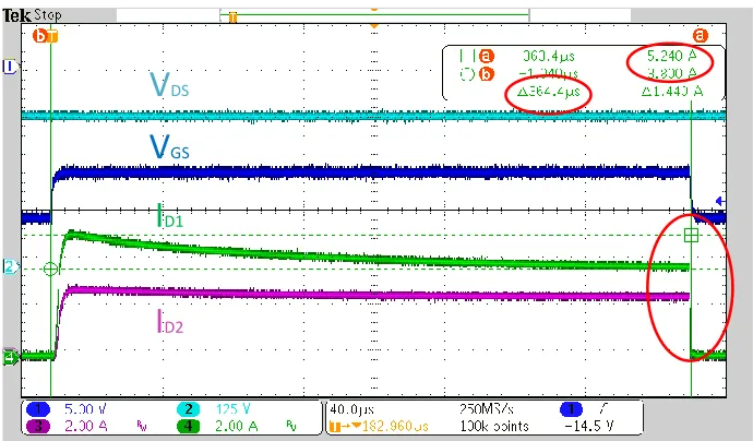
As analyzed above, the transient ID-TJ coefficient is very important during hiccup startup with multiple devices parallel. Figure 2.3 shows the test setup with different junction temperature and a typical saturation current waveform with short pulse test with minimum self-heating. The ceramic heat plate is used to heat the junction and a very short pulse (10us) is tested to avoid the temperature rise due to internal power dissipation.
Infineon ST
Wolfspeed USCi
In Figure 2.4, all four devices saturation current is listed under different junction temperature for same VGS in each device itself. The SiC JFET from USCi is the only device has the negative coefficient, which makes it the best option for dynamic current sharing during hiccup startup mode.
(a)
(b)
Figure 2.4 Saturation current vs. Junction temperature
I
D1I
D2V
GSV
DSFigure 2.5 to 2.7 shows the differences. The Fig. 2.5 shows the current sharing of paralleled Si CoolMOSTM under long pulse self-heating. The saturation current will increase and the current differences between two paralleled MOSFET will become larger, which is dangerous for hiccup startup with multiple devices parallel. The other two devices are similar to Figure 2.5.
Figure 2.6 shows the current sharing of paralleled SiC JFET under long pulse self-heating. The saturation current will decrease and the current differences between two paralleled SiC JFET will become smaller. It is a very good feature for hiccup startup with multiple devices parallel. Fig. 2.7 shows the continuous pulses current sharing of SiC JFET.
On the contrary, the SiC JFET has shown negative temperature dependency of the saturation current, which is desirable for current sharing during hiccup startup operation in solid state circuit breakers.
I
D1I
D2V
GSV
DSThe SiC devices in candidates obviously have a wider temperature range for safe operation compare with Si devices. And the SiC JFET normally on characteristic consumes lowest driver power compare with other three voltage driven MOSFETs.
The concern for SiC JFET is also its normally-on characteristic. The circuit breaker should be better in OFF state if the grid is from powered off to recover. The standard related to 380V DC solid state circuit breaker application need to be further defined by the whole system.
2.3.2 Characteristics for branch circuit breaker
Different from above application, the paralleled single piece solid state device won’t load
I
D1I
D2V
GSV
DSGenerally, the most important characteristic of solid state devices for branch circuit breaker applications is the turn-off capability. It can be interpreted as the maximum current rating that the device can turn off. This section presents comparative test results on turn-off capability of listed candidate devices for branch circuit breaker application in the 380VDC delivery system. Turn-off capability of each device is evaluated and compared for the first time. It also mimics the turn-off condition of the main switch in a DC hybrid circuit breaker as shown in Figure 2.8. The hardware setup is displayed in Figure 2.9.
Figure 2.8 Long Pulse Test Circuit for high current turn-off capability under 400V DC bus
Ids
Air-core
+
-+
-Vgs
Vds
All parameters, such as gate-to-source voltage (VGS) and external gate resistance (RG_external) are selected according to the datasheet of each device based on their normal operation, shown in Table 2.5. One exception is Wolfspeed C2M0025120D. Based on its datasheet, RG_external need to be 2.5Ω, but it results in large VDS overshoot and ringing under high IDS. Figure 2.10 shows the waveform of turn-off transient under 282A current, and VDS overshoot reaches 888V. For safety consideration, RG_external is increased to 5Ω, and its corresponding waveform shows that the VDS overshoot is 624V with much less ringing.
Figure 2.9 Hardware bench setup for high current saturation turn off test
DUT SiC diode
54uF DC cap
500uF DC cap
Fan
12V Power Supply 400V
Power Supply
Figure 2.11-2.14 shows the test waveforms for 4 candidates in long pulse over current saturation test with 400V DC bus voltage. The comparison with die size, peak power density, and other characteristics is listed in table 2.6.
Table 2.5 VGS and RG_external values for each device in long pulse test
Figure 2.11 Test results of Si MOSFET STY145N65M5 in high current saturation turn off test
104us
Vgs (20V/div)
Vds (100V/div)
Ids (200A/div) 688A
Vgs (20V/div)
Vds (100V/div)
Ids (200A/div) 688A
Figure 2.12 Test results of Si MOSFET IPW65R019C7 in high current saturation turn off test
72.6us
Vgs (20V/div)
Vds (100V/div)
Ids (100A/div) 524A
Vgs (20V/div)
Vds (100V/div)
Ids (100A/div)
250V
Figure 2.13 Test results of SiC MOSFET C2M0025120D in high current saturation turn off test
66us
Vgs (20V/div)
Vds (100V/div)
Ids (100A/div)
454A
Vds (100V/div)
Ids (100A/div) 454A
360V
Figure 2.14 Test results of SiC JFET UJN1205K in high current saturation turn off test
43.5us
Vgs (20V/div)
Vds (100V/div)
Ids (100A/div) 344A
Vds (100V/div)
Ids (100A/div) 344A
Vgs (20V/div)
In comparison, similarly with RDS(ON), the high current turn-off capability is related to die size. Moreover, the SiC also is better than Si devices in Ioff per area and Peak power density performance which has excluded the die size influence. In SiC devices, the SiC JFET is the best for characteristic needed for DC circuit breaker application. However, the naturally-on characteristic of SiC JFET needs the driver circuit to be carefully designed to have the breaker tripped off in a fault condition.
2.4 Conclusion and summary
In sum, the criteria of the characteristic for 380V DC circuit breaker is investigated and defined. Four devices are selected as candidates for 380V DC circuit breaker application. Comparison and evaluation of four devices have been analyzed and verified with experiment. The SiC devices perform much better and should be the best solution for DC circuit breaker
Table 2.6 Characteristics of Solid State Devices for Long pulse turn-off test
Type Manufacturer Part No. RDS(on)
@25 °C(mΩ) Ioff(A)
Die Size
(mm2) (A/mmIoff / A 2)
Peak P density (VA/mm2)
Si MOSFET Infineon IPW65R019C7 19 524 68.29 7.67325 2762.34
Si MOSFET ST STY145N65M5 14 688 121.88 5.6449 2032.16
SiC MOSFET Wolfspeed C2M0025120D 25 454 26.02 17.4481 6281.32
C
HAPTER
3
Hot Swappable Outlet for 380V DC System
3.1 Introduction and Motivation
Power outlets and power strips are needed for both traditional 120V/220V AC distribution system and proposed 190V, 270V or 380V DC distribution system. In AC system, the plugs and sockets are mature and regulated with different voltage and current ratings in different countries, such as IEC 60906-1 standard in Europe and NEMA standard in North America. Because of the zero crossing point in each half cycle in AC system, the electrical arc is not a severe problem for 120V or 220V voltage rating. [46]–[49]
However, the electrical arc has become a significant issue in DC power system due to lack of zero crossing point. The arcing and related potential risks of fire and human touch is a primary safety concern in the DC application.
3.2 State of Art DC Outlet
3.2.1 Saf-D-Grid® plug and receptacle
(a)
(b)
Figure 3.1 (a) Hardware configuration of Saf-D-Grid® Plug and Receptacle
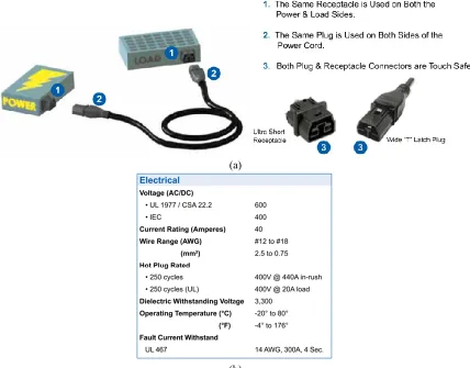
Currently, there are several solutions and products designed for 380V and similar DC voltage rating. Figure 3.1 shows the hardware and specifications of a Saf-D-Grid® [49]from Anderson Power Products®. The DC voltage and current ratings are 400V and 40A. The design is still optimized only on mechanical design. The designed short receptacle and long plug with Hi Temp Nylon and Polycarbonate housings contain the arc whether connectors are mated or unmated while under load to minimize the risk to operators. The first mate, last break ground contact and integral latch features are considered to enhance the safety and reliability.
3.2.2 FUJITSU DC outlet
3.2.3 PPTC solution from TE Connectivity®
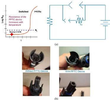
Figure 3.3 gives PPTC solution from TE Connectivity®.[48] PPTC stands for Polymer Positive Temperature Coefficient materials. It is a blend of polymer and conductive particles which can create a network of conductive paths. The resistance of PPTC increases with temperature rise.
(a)
(b)
Figure 3.2 (a) Hardware configuration of FUJITSU® DC Outlet
With such characteristics of PPTC, it is designed to be parallel with the main current path but with the first mate, last break connection. The current in PPTC heat itself to have current limiting capability. During unplugging, the PPTC reduce the final turn off current to shorten the arc between contacts into a safe region. Figure 3.3 (b) shows the comparison of tests results under 550V/20A DC.
(a)
(b)
3.2.4 Proposal from Virginia Tech
In 2011, CPES proposed a DC plug and socket in its DC Nano grid system.[51] Figure 3.4 gives more details. The basic idea is to treat the circuit as a buck converter. Extra power pin is necessary for driving circuit. For turn on, increasing the duty cycle makes the output voltage increase from 0 to Vin. For turn off, decreasing the duty cycle makes the output voltage decrease from Vin to 0. Only ideal circuit is proposed and simulated. Too many contacts are needed and the driver scheme is complicated. And the inrush current is not considered with SOA of solid state devices.
3.3 Design of Hot-Swappable Outlet
3.3.1 Circuit topology
The designed hot-swappable outlet is presented in Figure 3.5. Each socket is designed for 380V DC and 5A nominal current rating, which is about 2kW power rating. It covers most 2U to 4U power supply unit shown in Chapter 1. The earth wire is the default and ignored for showing more details in the diagram.
(+)
(-)
380V
DC BUS
Hot pluggable outlet
DC Load (e.g. Data Center) 1 Socket per server
(a)
Two major challenges to realize in developing hot pluggable outlet with solid state device in DC distribution system are the inrush current caused by the output bus capacitance in DC/DC converter (shown as in Figure 3.6 (b)) at the time of plugin and the arc discharge at the time of unplugging. The inrush current acts as a short circuit current because the voltage across the capacitor is zero at the moment we plug the bus capacitance into the source. [46] The inrush current is higher if the capacitive load is bigger and as a consequence, will damage the embedded device. It has to be limited in the safe operation area (SOA) of MOSFET when designing and developing the hot-pluggable outlet. The undesired arc discharge phenomenon in DC distribution system will have detrimental effects on both equipment and human safety. It can be avoided by cutting off the current with the embedded solid-state device before disconnecting the main circuit.
VGS Vgnd P N Energize (-)¹ N-MOS +380V Controller VDD DC/DC Vsen (+) (-) Load Plug (a) VGS Vgnd P N Energize (-)¹ N-MOS +380V Controller VDD DC/DC Vsen (+) (-)
Load Plug 380 DC / 48 DC
Output Bus C
3.3.2 Operation Modes Analysis for Hot Swappable Outlet
The operation modes are demonstrated in Figure 3.7. They are the standby mode, startup mode, normally on mode and unplug mode.
Standby mode: Before t1 and no load and plug, the whole circuit in the outlet is not powered since the energized pad is not connected. The NMOS is naturally open circuit because zero gate to source voltage. The power consumption in this mode is zero.
0V 380 0V 12V 8V 0V 8V 0V 8V 0V 8V VDS VGS
Start up Unplug
OFF VDD OFF VO_Cap 0 I*Rds(on) 380
0 0 0 0
VDD
ID
I load I load I*Rds(on) 380 12V
0
Normally On
t1 t2 t3 t4 t5 t6 t7
VDD
Normally on mode: The plug remains in position b in Figure 3.6. And the NMOS keeps fully turn-on to get lowest RDS(ON) to reduce power loss on solid state device.
Unplug mode: The plug is unmated and separated from energizing pad and the VDD becomes 0 at t5. The NMOS is off. There is only leakage current going through the device. The voltage of output capacitor will keep decreasing because of the working converter load until UVLO occurs. The drain to source voltage on NMOS will increase. At the moment of t7, the plug is fully unplugged with no arc because NMOS is off and only leakage current which is very small. There is also no inrush and arc for the energize pad as the total control circuit power consumption is only about 0.4W which is about 1mA steady state current consuming for 380V.
3.3.3 High Ratio Buck DC/DC Converter PSU
3.3.4 Dual Threshold Over Current Protection
Besides normal plugin and unplug features in the traditional outlet, the overcurrent protection on the negative bus can be also implemented at the same time which helps this outlet partially perform as a circuit breaker.
A dual threshold of overcurrent protection strategy is implemented by a controller to monitor over current or short fault. These two thresholds ILimit and ISC are adapted to trip the real over current fault and filter nuisance transient noises.
ILimit – Fault timer runs if ILoad>ILimit and the circuit breaker trip when the timer runs out of set up T(fault) which is usually been used to filter nuisance transient noises.
ISC – Short circuit threshold (typically 1.3 to 2.5 times of ILimit). ISC current limiting feature before final 1-10 us instantaneous trip.
ON
OFF
I I limit
I SC
T fault
ON
OFF
I I limit
I SC
Timer
3.3.5 Over Temperature Protection
An over-temperature protection is designed to limit the inrush hiccup cycles. The threshold is set with margin to 125 ̊C as the transient junction temperature is not accurately monitored in hot swappable outlet. The accurate junction temperature is monitored in Chapter 4 with more analysis and experimental results.
3.4 Experimental Results of Hot-Swappable Outlet
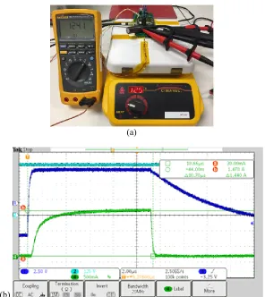
Figure 3.10 displays the developed hardware. The NEMA 6-20 T slot is a good candidate can be adopted because it naturally tells the positive and negative bus with two different shapes and the peak of 240V AC is close to 380V DC rating. The embedded circuit is about 1.5-inch square with one TO-247 MOSFET.
Figure 3.11 shows the waveforms from t1 to t5. The circuit spends about 3ms to start the 1.5 inch
1
.5
in
ch
Figure 3.12 presents the full waveform of hiccup startup mode. The inrush current is limited as about 9A as ID. The VGS is controlled for saturation to charge the output capacitor. The 47uF capacitor on output side takes about 70ms to be charged to 380V. This value can be programmed as long as the power stress of MOSFET is under SOA.
V
EnergizeV
DDV
GSV
DSFigure 3.11 Plug in process waveforms of DC hot pluggable outlet
ID VO_CAP
VDS
Figure 3.13 shows the thermal image in the steady state of 380V 5A normally on mode. The power loss is about 1W on this device with 33mohm RDS(on) and the hot spot is about 60.5 ̊C on the thermal pad.
Figure 3.14 shows the unplugging mode. After the energize pad disconnecting, it takes 56ms to fully power off the control circuit and turn off the MOSFET. This value can be reduced by decreasing the capacitance in power supply circuit.
Figure 3.13 Normally on Steady state thermal image
V
EnergizeV
DDV
GSFigure 3.15 shows the waveforms of dual threshold overcurrent protection. From waveforms, we can find that once the sensed current is over Ithreshold (=5.2A), the controller will trip the circuit after the preset tfault (=680us) timer. Once the controller decides to trip, the circuit only spends about 1us to finish this process like an instantaneous trip.
Figure 3.16 shows the instantaneous threshold trip with high current.
VDS
ID VGS
Figure 3.15 Lower threshold with timer over current protection waveforms of DC hot pluggable outlet
VDS
ID VGS
Figure 3.17 gives the waveforms of over temperature protection. From waveforms, we can find that once the sensed temperature reaches 100 ̊C (1.23V from Vo of sensor), the circuit will be tripped by the controller in about 1.68 us.
3.5 Conclusion and Summary
In sum, a hot-pluggable outlet is proposed and developed for 380V DC distribution system. There are several novel and useful features as follows:
1. The standby power of the outlet is zero because there is no drive power needed and gate voltage can be naturally pulled down to 0V to turn off the embedded MOSFET. The input power for buck converter is zero since the energize pad is not connected during standby.
VTemp
VDS
ID
VGS
VTemp VGS
VDS
ID
2. The mechanical structure is novel and simple. The energize pad which is designed at the bottom of the socket makes the plug compatible with traditional 3 pole system (one is earth). Only one pole is used to shorten the positive bus and energize pad. Meanwhile, the bottom energizing pad naturally implements “the last energize, first de-energize” for protecting and safety of device and operator. The similar mechanical structure can be optimized to replace a simple pad as long as the contact sequence is same.
3. The embedded solid-state device helps to limit the inrush current and eliminate the arc with low power consumption. The total power loss from the control circuit and MOSFET are about 1.4W under 380V, 5A which is about a 2kW load.
4. The dual threshold current trip can be realized because of the embedded MOSFET. It notably helps in preventing short circuit and other faults in DC downstream.
5. Under voltage lockout on input bus voltage is designed for isolating the downstream load from the bus for protecting both bus voltage on upstream and load on downstream. 6. Over-temperature protection is designed and embedded for protecting the solid-state
C
HAPTER
4
Solid State Circuit Breaker for 380V DC System
4.1 Introduction and Motivation
As stated in Chapter 1 and 2, the circuit breaker is a mandatory component and has a significantly vital position in 380V DC power system. The mechanical circuit breaker and fuses are still being used in DC system protection nowadays. The problem of this kind of circuit breaker is the trip speed cannot meet the requirement of system protection in DC system. The trip current threshold is too large compared with the nominal current rating and the speed is almost above 10ms. Another challenge is the arc during contacts breaking in DC system, which limits the lifetime of the mechanical circuit breaker.
In this chapter, a solid-state circuit breaker with paralleled devices is proposed, designed and analyzed. The interleaved startup strategy is introduced to improve the thermal stress sharing for reducing the system unreliability. It is also a benefit for enhancing the speed of startup. Additionally, a novel real-time junction temperature monitoring strategy is proposed, analyzed and tested for protecting the embedded solid-state device.
4.2 State of Art DC Circuit Breaker
4.2.1 CX-series DC circuit breakers
(a) (b) Figure 4.1 (a) Hardware configuration of CX-series DC circuit breaker
Figure 4.1 shows the latest Hydraulic/Magnetic Circuit Breaker designed specifically for 380V DC system[53]. It has been optimized mainly for solving the arc issue in DC system. Permanent magnets combined with the upper and lower arc runner increase the magnetic blow out force and aid in motivating the arc off of the contacts and into the arc chamber. The arc chamber features arc splitter retainers with integrated pressurizing walls, which facilitates heat transfer from the arc providing additional cooling and allowing quick transition into the magnetically induced by splitter plates. [53]
4.2.2 Ultrafast autonomous SiC JFET circuit breaker
(a)
(b)
(c)
Figure 4.2 shows a self-powered circuit breaker with SiC JFET.[54] As described in Chapter 2, the SiC JFET is very competitive because of its large short circuit current capability and negative temperature coefficient. In the current design, the author utilizes the voltage drop on the device for large fault current (>100A). The 4.5V voltage drop (45mOhm RDS(ON)) is used to provide a voltage supply for the local isolated driver circuit to generate a negative VGS to turn off the normally on SiC JFET. This period could be very fast and less than 1us.
The self-power is the most appealing and innovative feature of this paper. The drive circuit needs no power for the normal operation because of the normally on SiC JFET.
However, the self-power needs two latent premises. The multiplication of the RDS(ON) and threshold current need to be large enough to energize the drive circuit. But for products in the real world, both two parameters are the smaller the better.
4.2.3 400V DC SiC-SIT circuit breaker by NTT Japan
(a) Dimension of SiC-SIT CB: 45 mm(W) 100 mm(H) and 370 mm(D)
(b)
(c)
Figure 4.3 (a) Hardware of SiC-SIT NTT DC circuit breaker (b) Circuit schematic configuration
In figure 4.3, a SiC-SIT DC circuit breaker developed by Chiba University and NTT Japan is displayed.[55] The power rating is 400V/12.5A. The most important feature is the programmed slope gate drive voltage for suppressing the overvoltage on VDS during turn-off. Without local snubber circuit, the overvoltage spike can be 950V for only 2.4A turn-off due to large line inductance. With proposed slope gate drive voltage, this overvoltage can be remarkably reduced to 660V with 6A turn-off current and 140uH line inductance. As a result, the price is the increased turn-off speed which is approximate to 22uS.
4.3 Hardware Design and Analysis
4.3.1 Circuit topology
The main circuit of the designed solid-state circuit breaker for 3 wire 2 phase 380V DC system is shown in figure 4.4.
1. Two paralleled solid-state device modules are located on positive and negative buses for limiting and tripping the current flow.
2. A µController is embedded to control the circuit and make all parameters programmable.
3. Input capacitors and freewheeling diode on the output side is designed to minimize
(+) (-) P N E +190V -190V +380V DSP Input Output Paralleled SSCB V I I I I I I
4. The operation modes are similar to the one in Chapter 3 with inrush startup, normal operation, and dual current thresholds trip.
4.3.2 Interleaved hiccup startup with inrush current strategy
As demonstrated in Chapter 2, most solid-state devices have a positive feedback on saturation current and junction temperature. During paralleled operation, this characteristic will make the saturation current diverge under same gate voltage. The device with the largest saturation current at the beginning will fail in a short period although all other devices are still under low thermal stress.
t1 - t2: The whole circuit starts the startup process with saturation current limitation. The paralleled solid-state devices work under saturation mode with closed-loop control till t2. The output voltage keeps rising due to the limited saturation inrush current. This makes the drain to source voltage on paralleled devices keeps decreasing.
OFF ON OFF Paralleled MOSFET 3 OFF Paralleled MOSFET 1 OFF OFF OFF OFF OFF OFF OFF OFF ON ON Paralleled MOSFET 2 380 0 I*Rds(on) 380
t1 t2 t3 t4 t5 t6
V
DSV
O_Capt2 – t3: All devices are fully turned off because every device is still in cooling mode due to large thermal stress come with saturation pulse. This period is the shorter the better, although still limited by thermal limitation. Both voltages keep the same value as only leakage current exists.
t3 – t4: Interleaved saturation pulses start to repeat again because the cooling mode ends for the first device. It is the repeat stage of t1 - t2.
t4 – t5: All devices are fully turned off because all of them are in cooling mode. It is also the repeat stage of t1 - t2.
t5 – t6: The interleaved startup repeats again and again until the output voltage reaches input bus voltage. All devices are fully turned-on with high VGS because the saturation mode is no more needed and the VDS is already equal to ID×RDS(ON)
4.3.3 Transient and steady-state real-time junction temperature monitoring
In this design, the junction temperature of solid state devices changes in a large range during inrush startup. And for most of the operation period, the normally on operation is the dominant mode. One major reason fails the solid-state devices is the thermal stress. So, the reliability of device could be significantly enhanced if the junction temperature is monitored accurately.
Figure 4.6 exhibits the saturation curves of the same IPW65R019C7 from Infineon CoolMOSTM. All other devices have a similar characteristic with the exception of the SiC JFET being on opposite trend, which is introduced in Chapter 2.
From this figure, it is evident that the saturation current is associated with the junction temperature, gate voltage VGS and drain to source voltage VDS.
𝐼𝐷 = 𝑓(𝑇𝐽, 𝑉𝐺𝑆, 𝑉𝐷𝑆) (4.1)
Obviously, the junction temperature can also be derived as:
𝑇𝐽 = 𝑓(𝐼𝐷, 𝑉𝐺𝑆, 𝑉𝐷𝑆) (4.2)
Once constant I startup is utilized within designed SOA, there is one parameter which can be neglected, making equations 4.2 to 4.3.
𝑇𝐽 = 𝑓(𝑉𝐺𝑆, 𝑉𝐷𝑆) (4.3)
For steady state, one important parameter RDS(ON) helps us to monitor junction temperature, which is widely used to sense ID in other applications. Figure 4.9 shows such characteristic.
In figure 4.8, the low temperature-coefficient sensing resistor is designed and applied to sense the drain current. Once the accurate ID is known, the VDS can be measured to calculate the RDS(ON) and then the junction temperature during steady state is obtained.
4.3.4 High impedance fault protection
The high impedance fault is a challenge for system protection. It is always treated as regular load by circuit breaker which usually causes a fire hazard with high impedance
Thanks to the symmetrical 3 wires 2 phase circuit breaker design, the high impedance fault between positive and ground, negative and ground can be sensed and protected as a result of the unbalanced line currents on positive and negative buses.
4.4 Experimental Results of Solid State Circuit Breaker
4.4.1 Hardware design
Each device is equipped with its own input snubber capacitor, output freewheeling diode, current sensor and driver circuit which make them a single module and easy to scale up.
The power density is about 20W/cm3 for 380V (±190V) and will be larger when applied with ±380V.
4.4.2 Interleaved hiccup startup with inrush current strategy
The hardware of solid state circuit breaker has been developed with 2 groups of paralleled MOSFET to share specified current to reduce the thermal stress under steady state. However, as analyzed in 4.3.2 and Chapter 2, the inrush current need to be considered with interleaved hiccup strategy due to the positive temperature coefficient during transient current sharing.
In figure 4.10, an interleaved hiccup startup for 190V positive DC bus with 100uF capacitive load and 10A constant current closed-loop control is shown. In each group, 4 devices are closed-loop controlled with constant 10A as figure 4.7.
Figure 4.11 shows one group of saturation current closed-loop control on 10A with 200uS pulse width on every single MOSFET. The gate voltage of the 1st and 4th device is shown in channel 1 and channel 3. They are controlled with an adaptive voltage with DAC on DSP and a related analog drive circuit. The delay of each interleaved pulse is controlled as 500uS.
Figure 4.10 Interleaved hiccup close loop startup waveform for 190V/100uF/10A
Vout
Vgs1
Vgs4
Figure 4.12 shows the time delay of each group is 10mS. This delay is the cooldown time for the single device to control the thermal stress. All parameters stated above, such as 10A, 200uS pulse width, 500uS pulse delay and 10mS cooldown time, can be programmed and modified under different load condition.
Figure 4.11 Zoom in multi-channel close loop constant ID control waveform Vout
Vgs1
Vgs4
4.4.3 Steady-state thermal performance
For solid state circuit breaker, most of the working time is normally conducting. So, the temperature rises under heavy load and high current need to be tested.
Figure 4.12 Cooldown interval of each group
Vout
Vgs1
Vgs4
Figure 4.13 shows the hardware bench setup and DC power supply.
As shown in figure 4.14, the steady-state temperature on the heatsink is about 50.3C after 40 minutes with 20C room temperature. It is a safe temperature for human touch. It also means there is enough margin for some other application with severe temperature conditions such as summer in Arizona.
So, the power loss on every single MOSFET can be calculated as in equation 4.4:
𝑃𝑆𝑖𝑛𝑔𝑙𝑒 𝑀𝑂𝑆𝐹𝐸𝑇 = 𝐼2𝑅
𝐷𝑆(𝑜𝑛)𝑇_𝑑𝑖𝑒 = 7.5𝐴2× 17𝑚𝑂ℎ𝑚 × 1.3 = 1.243𝑊 (4.4)
The junction temperature can be derived with thermal resistance and heatsink temperature:
𝑇𝐽𝑢𝑛𝑐𝑡𝑖𝑜𝑛 = P ∗ 𝑅𝑡ℎ(𝐷𝑖𝑒−𝐻𝑒𝑎𝑡𝑠𝑖𝑛𝑘)+ 𝑇𝐻𝑒𝑎𝑡𝑠𝑖𝑛𝑘
= 1.243𝑊 × (0.2 + 0.35)℃
𝑊+ 50.3℃ = 51℃
4.4.4 Dual threshold overcurrent protection
Similar to design in Chapter 3, the dual threshold overcurrent protection can be also applied to solid state circuit breaker. The DSP calculates the total current flow through 4 paralleled MOSFET and turns off the circuit with programmed time delay. In Figure 4.16, it shows the test results for lower threshold overcurrent protection. The threshold is 32A and load is set to 38A to verify the protection.
Figure 4.17 shows the gate voltage change from 12V to -2.5V to trip the breaker.
In figure 4.18, the solid-state circuit breaker is tripped with adaptive ramp down digital to analog circuit with 10us time constant to reduce the voltage stress on solid state device. Both current threshold and this ramp speed are also programmable.
In figure 4.19, the high threshold overcurrent protection is demonstrated. The current threshold is programmed as 50A. Once the current hit the high threshold, the solid-state circuit breaker starts the adaptive gate voltage control to saturate the circuit and limit the current with a 200us time delay.
Figure 4.19 High threshold OCP with saturation current close loop control 6.6V
4.4.5 Transient real-time junction temperature monitoring
In the previous description, the junction temperature of the solid device in the transient state can be monitored with equation 4.3 when the saturation current is closed-loop controlled during transient startup.
An experiment has been carried out to verify this proposal. The drain current is set to 7.5A on single device STY139N65M5. The equation 4.6, yields,
𝑉𝐺𝑆 = 𝑓(𝑇𝐽, 𝑉𝐷𝑆) (4.6)
Figure 4.21 briefs the experiment, which helps us get obtain the equations 4.3 and 4.6. The short pulse VGS is adopted for getting saturation current ID=7.5A under various junction temperature TJ and drain to source voltage VDS.
From multiple short pulse tests, a group of data points can be obtained. Corresponding 3D curve fitting is given in figure 4.23.
Figure 4.21 Short pulse test with 7.5A ID and different TJ and VDS
Although some of the data points are not on the fitting surface of the linear model above, the equations still have the edge for DSP easily processing with fast speed to implement real-time monitoring.
Figure 4.24 gives the VGS and VDS of first saturation pulse with ID=7.5A being constant. The VGS changes from 5.50V to 5.38V as both junction temperature and the drain to source voltage change on the 3D surface.
The monitored junction temperature is in figure 4.25. The result indicates that the junction temperature changes from 36.28 ̊ C to 60.99 ̊ C in coordinated 421us. This monitored temperature can be examined with transient thermal impedance of used device. The comparison is given in figure 4.26.
(a)
Figure 4.24 VGS and VDS of first saturation pulse
![Figure 1.7 15A MCCB trip curve[27]](https://thumb-us.123doks.com/thumbv2/123dok_us/1349919.1167870/22.612.203.425.293.552/figure-a-mccb-trip-curve.webp)