Design and Simulation of Low Power Wide
Range Bidirectional Level shifters
Sreekumar R, Reshmi P B
Assistant Professor, Dept. of ECE, Govt Engineering College, Idukki, Kerala, India1
PG Student (VLSI), Dept. of ECE, Govt Engineering College, Idukki, Kerala, India 2
ABSTRACT: Level shifter converts digital signals from one standard logic level to other. Wide-range level shifters play critical roles in ultralow-voltage circuits and systems. Although the existing level shifters can convert a subthreshold voltage to the standard supply voltage, they may have limited operating ranges. Therefore a new level shifter, of which the operating range is from a deep sub threshold voltage to the super threshold voltage and includes upward and downward level conversion. The proposed level shifter is a hybrid structure consisting a modified Wilson current mirror and generic CMOS logic gates.
The result is a bidirectional level shifter in 90 nm technology with minimal operating voltage was less than 100 mV. The proposed level shifter has the power dissipation of 287nW for 200mV to 1200mV conversion. And propagation delay of the proposed level shifter circuit also reduces to 46.9nS.
KEYWORDS:Level shifter, stacking, Wilson current mirror, Power consumption. .
I.INTRODUCTION
Level shifter (LS) is a interfacing circuit which can interface low voltage to high input-output voltage. They are also called voltage translator. In the present devices like mobile phone, battery powered electronic systems consists of more and more circuit that may be designed on a single chip. But the operating range of these circuits are different. Therefore level shifter circuits are necessary. Low power dissipation is the one of the important design criteria of high performance level shifter. However conventional level shifters have disadvantage of large power dissipation, delay issues and circuit fail to operate at low supply voltage [2] [1].
The growing market devices especially in the case of portable devices demand the design of microelectronic circuits with low power dissipation. Hence low power dissipation level shifter with low input voltage is very important. The subthreshold operation is the emerging method to achieve ultra-low power consumption.it leads to the development of some crucial application like intelligent sensors, miniature health care devices. Subthreshold operation are limited to the part of digital processing elements [8]. It also contain other system components that have distinct supply voltage constraints, where sub to suprathreshold level conversion is unavoidable. General purpose application also require wide range level shifters mainly in the case of dynamic voltage scaling applications.
II.LEVEL SHIFTERS
Small area for sub threshold level conversion.
Low power consumption in super threshold Operations.
Balancing rising and falling delay in the operating Range. Bidirectional level conversion.
Size & Vth Insensitivity.
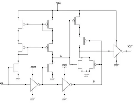
In this paper proposed level shifter is compared with two different level shifters. The existing LS is a hybrid structure consist of a modified Wilson current mirror and CMOS logic gates. Here sub-threshold voltage to the standard supply volt-age conversion is possible. This gives the better performance and the low power consumption based level shifter for dynamic voltage scaling applications. Fig 1 shows the modified Wilson current mirror based level shifter. The LS circuit contains 3 blocks, first the modified Wilson current mirror circuit, second delay circuit and third one is CMOS OR gate for the level shifting operation. For this type of level shifter the standard and sub-threshold voltages are given to the circuit. The standard supply voltage (VDD2) is given to Wilson current mirror circuit and the sub-threshold voltage (VDD1) is given to the inverter. Modified Wilson current mirror is located with the help of 4 transistors which balance the rising and falling delay of circuit. But when the input and output levels are close to each other there is a problem of skews. That is caused by insufficient drive current of cascade PMOS transistors which increases rising delay. This rising delay compensated by the delay circuit consisting of two inverters which acts as buffers. CMOS OR gate circuit provide proper output and limits the leakage current.
Fig. 1. MWCMHB level shifter.
The operating condition of MWCM based LS is given below. When Vin increases, rising signal at Node A and B achieves trip point voltage more quickly determine the rise of the output signal.in the case of up conversion voltage signal at node A achieves trip point first. That is VDD2 is higher than VDD1+V.where V is the voltage drop related to MWCM output. The MWCM has similar rising and falling delays. When Vin falls, voltage at node A and B must be low in order to trigger the fall of output. But the falling signal at node A is slow because of the NMOS length of MWCM is upsized to reduce mismatch. Therefore falling of Vout waits falling signal at Node A to achieve trip point. The two inverter used to balance the rising and falling delays when VDD2 is less than VDD1[8].
A. POWER REDUCTION METHODS
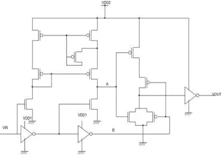
Wilson CM based LS to reduce power [7]. Out of which stacking technique shows better performance. Fig 2 shows modified Wilson CM based LS using stacking technique.
In stacking technique pull down network is not modified. Only pull up network is modified by stacking approach. In the existing LS PMOS transistors in the CMOS OR circuit splits into two each transistor having size half of that existing transistors. When two transistors are turned off together which induced reverse bias condition between two transistors results reduction in leakage power. The leakage through two series off transistors much lower than that of single transistor because of stacking effect [10].
Fig. 2. MWCM based LS using stacking technique.
III.PROPOSED LEVEL SHIFTER
IV.RESULTS AND COMPARISONS
This section presents results and comparison of delay, power of proposed and reference level shifters. The proposed and reference LSs are simulated using a 90 nm technology. For a fair comparison of circuit structure, the key transistors used the same Vth, width and length. The sizes were assigned for MWCM based LS as follows,
Wp/Lp of MWCM circuit =400nm/150nm Wp/Lp of CMOS OR gate = 200nm/150nm Wn/Ln =350nm/150nm
Wp/Lp of inverter = 200nm/150nm
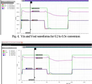
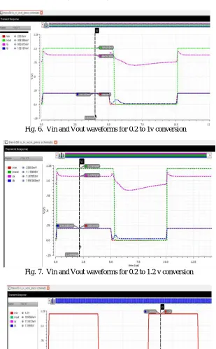
Wn/Ln of inverter = 120nm/150nm this lS modified using stacking technique in order to reduce leakage power. All the transistors having the same size except PMOS transistors in CMOS OR gate. All the PMOS transistors in CMOS OR gate are resized to 120nm/150nm according to stacking technique.in the proposed circuit all NMOS and PMOS transistors are resized to 120 nm/200nm except for inverters. Inverters are resized as follows Wp/Lp of inverters = 200nm/200nm Wn/Ln of inverters =120nm/200nm Fig 4-8 shows four simulation waveforms of the proposed LS. The input level is constant at 0.2V.the output levels are 0.5V,0.8V, 1V and 1.2V .The input frequency is 100kHz. The rising signal at node A triggers the output in all cases .the high signal at node A is VDD2-V which triggers the output voltage in most cases. When VDD2 low a weak voltage trigger he rise of output as shown in the first case. Fig 7 shows simulated waveform for downward conversion. Where the input voltage is 1.2V and output is 0.2V.in the proposed level shifter the range of conversion also increased ie from 0.1v to 1.2 v and vice versa.
Fig. 4. Vin and Vout waveforms for 0.2 to 0.5v conversion
Fig. 6. Vin and Vout waveforms for 0.2 to 1v conversion
Fig. 7. Vin and Vout waveforms for 0.2 to 1.2 v conversion
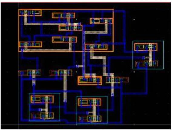
Table 1 shows the details of power consumption for all range conversion. A power consumption rise observed for converting deep sub threshold voltage. This high power consumption caused by the slow input slew rate. The proposed level shifter having area of 12.5u by 10.9u as shown in Fig10.
Table 1. Average power consumption diagram for all conversions
Fig. 10. Complete layout of the proposed LS
A. COMPARISONS
Fig. 11. Vin and Vout waveforms for 1.2 to 0.2v conversion Fig. 12. Vin and Vout waveforms for 1.2 to 0.2v conversion
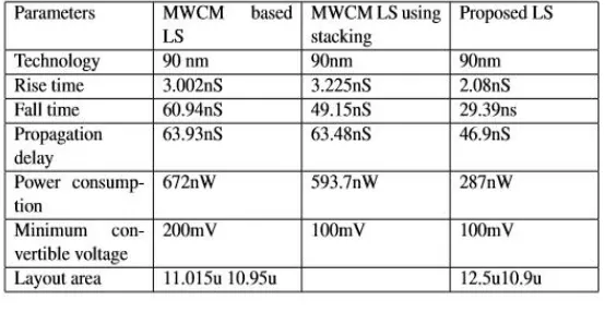
Table 2. Comparison
VI.CONCLUSION
In this work effort is made to understand various topologies of existing level shifter circuits and identify the limitation in these circuits. The bidirectional wide range level shifter for low power consumption applications was designed to produce a power consumption of 287nW for sub threshold to super threshold range ie for 200mV to 1200mV range. Here the minimum operating voltage in 100mv.Propagation delay of the proposed level shifter circuit also reduced from 63.48nS to 46.9nS.The delay, power consumption, rise time and fall time of proposed level shifter were verified for the full range operability. The power consumption of the proposed level shifter is verified using 90nm technology.
REFERENCES
[1] A. Hasanbegovic and S. Aunet, Low-power subthreshold to above thresh-old level shifter in 90 nm process, in Proc. Conf. NORCHIP, pp. 14,2009.
[2] ] S. Ltkemeier and U. Rckert, A subthreshold to above-threshold level shifter comprising a wilson current mirror, IEEE Trans Circuits Syst. II, Exp. Briefs, vol. 57, no. 9, pp. 721724, Sept. 2010.
[3] Chang, J. Kim, K. Kim, and K. Roy, Robust level converter for subthresh-old/ super-threshold operation:100 mV to 2.5 V, IEEE Trans. VLSI Syst, vol. 19, no. 8, pp. 14291437, Aug. 2011.
[4] ] Y. Osaki, T. Hirose, N. Kuroki, and M. Numa, A low-power level shifter with logic error correction for extremely low-voltage digital CMOS LSIs, IEEE J. Solid-State Circuits, vol. 47, no. 7, pp. 17761783, July 2012.
[5] M. Lanuzza, P. Corsonello, and S. Perri, Low-power level shifter for multi-supply voltage designs, IEEE Trans Circuits Syst. II, Exp. Brief , vol. 59, no. 12, pp. 922926, Dec. 2012.
[7] Harshvardhanupadhyay Comparison among different CMOS inverter with stack keeper approach in VLSI design, IJERA vol.2, issue 3,, , pp.640-646, May-Jun 2012.
[8] S. C. Luo, C. J. Huang, and Y. H. Chu, A wide-range level shifter using a modified wilson current mirror hybrid buffer, IEEE Trans. Circuits Syst. I, Reg. Papers , vol. 61, no. 6, pp. 16561665, Jun. 2014.
[9] Raj Kumar Tiwari, Sachin Kumar and G R Mishra ,a study on techniques of improvement in current mirrors using Wilson scheme. IJECET ISSN, 2012 Volume 3, Issue 2.
[10]Sehunkim Sleepy keeper: a new approach to low-leakage power VL.
[11]A vignesh “Performance analysis of various Level shifters using LECC,” International Journal of advanced research in electrical vol.2, issue 4, April 2013.