Comparative Study of Seven Level Boost
Inverters Using Sinusoidal Multicarrier PWM
Technique
Bhagyalakshmi P S1, Beena M Varghese2 , Jeena Joy3
PG Student, Dept. of EEE, Mar Athanasius College of Engineering, Kothamangalam, Kerala, India 1 Professor, Dept. of EEE, Mar Athanasius College of Engineering, Kothamangalam, Kerala, India 2, 3
ABSTRACT: This paper presents the comparative study of various seven level Boost inverters using Multicarrier Pulse Width Modulation technique. Conventionally, Seven Level Boost inverter can be generated by cascading three full bridge inverter in series. The maximum output voltage generated from the cascaded inverter is the sum of dc voltage values of the three full bridge inverter cells. Another boost inverter output generation is from the switched capacitor multilevel inverter. There are three different switched capacitor topologies are exist. Switched capacitor multilevel inverter gives higher voltages than the input dc voltage with help of series-parallel conversion operation. The maximum output voltage is the sum the voltage across the capacitors and input dc source voltage. In this work, above four boost inverter topologies are studied using the sinusoidal PWM technique based on the THD spectrum and device count. Simulation of multilevel inverter circuit is carried out using MATLAB/Simulink.
KEYWORDS: Cascaded multilevel inverter, switched capacitor multilevel inverters (SCMLI), Multicarrier PWM Technique, Total Harmonic Distortion, Output Voltage, Output Current.
I. INTRODUCTION
In recent years, electrical energy systems, electric vehicles, dispersed generation and renewable energy sources like PV, fuel cell etc are focused & plays a vital role against the global environmental issues. As a provision of this issue, multilevel inverters have gained much attention in recent years due to its advantage in high power with low harmonic applications. Multilevel inverters produce a staircase output voltage waveform, which is similar to that of sinusoidal waveform.
Multilevel inverters produce a stepped output phase voltage with a refined harmonic profile when compared to a two-level inverter. The concept of multitwo-level inverters, introduced about 30 years ago, entails performing power conversion in multiple voltage steps to obtain improved power quality, lower switching losses, better electromagnetic compatibility, and higher voltage capability. Nowadays, there exist three commercial topologies of multilevel voltage source inverters: the most popular being the diode-clamped, flying capacitor and cascaded H-bridge structures. These multilevel inverters with more number of levels are more efficient than the conventional two level inverter, but it has some drawbacks like requirement of more no of switching devices, manufacturing cost etc. Some of the topologies like the cascaded H- bridges uses multiple number of sources to obtain higher levels of output. The diode clamped or neutral point clamped has the difficulty of increase in the number of clamping diodes as level increases. Similarly, in case of flying capacitor multilevel inverter the number of capacitors increases and system becomes bulkier [6]. Among these inverter topologies, cascaded multilevel inverter reaches the higher output voltage and power levels, and the higher reliability due to its modular topology and the simplicity. In all the above topologies, the peak amplitude value of the output will be only the source voltage, with the rest of the levels being only a fraction of input voltage.
the input voltage sources are connected in parallel, the capacitors are charged. When the several capacitors and the input voltage sources are connected in series, the capacitors are discharged. The charge pump output the sum of the voltages of the capacitors and the input voltage sources [1] [3].
Multilevel inverter possesses the advantage of reduced harmonics, high-power and high-voltage capability. The multilevel inverters are mainly controlled with sinusoidal PWM technique and the harmonic contents can be reduced by using multicarrier PWM techniques. The multicarrier pulse width modulation cascaded multilevel inverter strategy enhances the fundamental output voltage and reduces total harmonic distortion. Multilevel inverters include an array of power semiconductors and capacitor voltage sources, the output of which generate voltages with stepped waveforms. In this paper inverter introduced which outputs larger output voltage with help of switching capacitors in series and parallel is analysed with help of different PWM techniques and analysed for the less total harmonic distortion (THD) less voltage ripple in output voltage and effective reduction in losses.
II. CASCADED SEVEN LEVEL INVERTERS
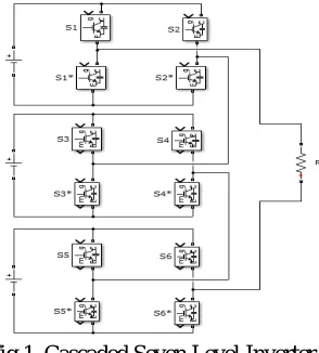
Conventionally, seven level inverter is by cascading the similar full bridge inverter in series. A single phase full bridge inverter gives 3 level stepped inverter output. (2n+1) levels are obtained from cascading n number of single phase full bridge inverters. In this work 3 full bridge inverters are cascaded in order to generate 7 output levels and the maximum voltage is n.Vdc = 3Vdc .Fig 1 shows the 7 level cascaded full bridge inverter.
Fig 1. Cascaded Seven Level Inverter
As the number of levels increases the output more approximated to sinusoidal signal, THD spectrum thus improved. Another advantage of cascaded inverter is that the output is more than the input dc voltage. Disadvantages of cascaded inverter are that it requires separate dc sources for three different full bridge inverter cells. And also single full bridge consists of four power switches. So cascading connection increases number of power switches, here 12 switches are used.
III. SWITCHED CAPACITOR MULTILEVEL INVERTER
A. TOPOLOGY 1
In Switched Capacitor Multilevel Inverter Topology 1, switched capacitor cell consists of three power switches and one capacitor. Each cell is connected in parallel and series by switching the power switches alternately.
Fig 2 shows the circuit diagram of switched capacitor multilevel inverter.
Fig 2. Switched Capacitor Seven Level Inverter Topology 1
B. TOPOLOGY 2
In Switched Capacitor Multilevel Inverter Topology 2, switched capacitor cell consists of two power switches, one diode and one capacitor. Each cell is connected in parallel and series by switching the power switches alternately. Fig 3 shows the circuit diagram of switched capacitor multilevel inverter.
Fig 3. Switched Capacitor Seven Level Inverter Topology 2
C. TOPOLOGY 3
Fig 4. Switched Capacitor Seven Level Inverter Topology 3
IV. CONTROL STRATEGY
To synthesize multilevel output AC voltage using different levels of DC inputs, semiconductor devices must be switched ON and OFF in such a way that desired fundamental is obtained with minimum harmonic distortion. There are different types of approaches for the selection of switching techniques for the multilevel inverters.
In this work Multicarrier Sinusoidal Phase Disposition PWM method is employed and all the carriers are in phase with each other. And all the carriers have the same frequency and amplitude. This method uses (n-1) carrier signals to generate n- level inverter output voltage. It is based on the comparison of a sinusoidal reference waveform with vertically shifted carrier of higher frequency.
The reference waveform has amplitude Am and frequency fm and placed at zero reference. The reference wave is continuously compared with each of the carrier signals. If the reference wave is more than a carrier signal, then the active devices corresponding to that carrier are switched ON. Otherwise, the device switched OFF. Switching pulses are generated by comparing the six carriers with the low frequency modulating wave. Pulse instant is determined by the instant at the cross over points between the modulating and carrier wave. When sinusoidal wave is greater than the carrier, then pulse is created.
Fig 5. Multicarrier Sinusoidal Phase Disposition PWM
A. SIMULINK MODEL FOR PULSE GENERATION
Fig 6. Switching Pulse Generation Subsystem
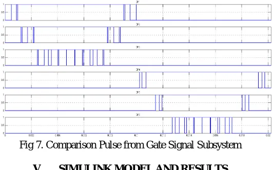
Switching pulses are generated using logical functions (OR, NOT) of the six comparison outputs (CP1,CP2...,CP6). Figure shows the six comparison outputs.
Fig 7. Comparison Pulse from Gate Signal Subsystem
V. SIMULINK MODEL AND RESULTS
Simulation is done with following parameters as shown in TABLE 1. MOSFETs are used in place of switching devices. Table 1. Simulation Parameters
Parameters Value
Input voltage 5V Switching frequency 1.6 kHz
Carrier Amplitude 1 units Modulating frequency 50Hz Modulating Amplitude 3 units
A. SIMULINK MODEL
Fig 8. Simulink Model of the Cascaded Seven Level Inverter
Fig 8 shows the simulink model for the Cascaded Seven Level Inverter. Gate pulse subsystem generates the switching pulses to the respective switches. Output current and voltage are measured separately and THD is measured using THD block.
Fig 9 shows the simulink model for the Switched Capacitor Multilevel Inverter Topology 1. Gate pulse subsystem generates the switching pulses to the respective switches. Output current and voltage are measured separately and THD is measured using THD block.
Fig 9. Simulink Model of the Switched Capacitor Seven Level Inverter Topology 1
Fig 10. Simulink Model of the Switched Capacitor Seven Level Inverter Topology 2
Fig 11 shows the simulink model for the Switched Capacitor Multilevel Inverter Topology 3. Gate pulse subsystem generates the switching pulses to the respective switches. Output current and voltage are measured separately and THD is measured using THD block.
B. SIMULATION RESULT
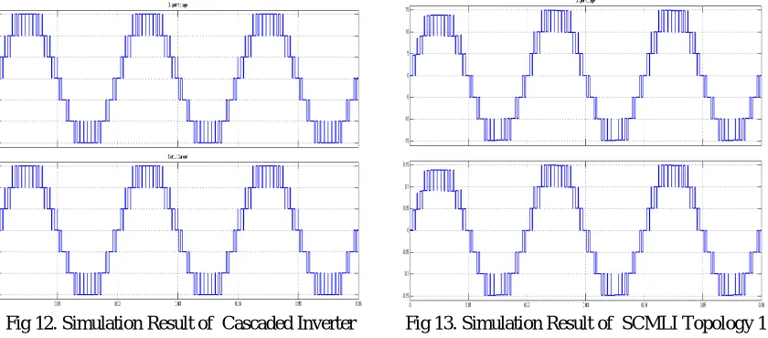
Figure shows the output voltage and output current of the above four circuits. Voltage and current are in phase because of the resistive load of 100ohm is used for simulation.
Fig 12. Simulation Result of Cascaded Inverter Fig 13. Simulation Result of SCMLI Topology 1 Fig 12 shows the output voltage and current of Cascaded Seven Level Inverter. Here the output is 15V from a 5V dc input. Output current is 0.15A for a 100ohm resistive load.
Fig 13 shows the output voltage and current of Switched Capacitor Topology 1. Here also output voltage is 15V from a 5V dc input. Output current is 0.15A for a 100ohm resistive load.
Fig 14 shows the output voltage and current of Switched Capacitor Topology 2. Here output voltage is some volt less than15V from a 5V dc input. Output current is 0.13A for a 100ohm resistive load.
Fig 15 shows the output voltage and current of Switched Capacitor Topology 3. Here output voltage and output current is less than 15V expected. But this topology possesses less switching devices compared to rest three seven level circuits.
VI. COMPARATIVE STUDY
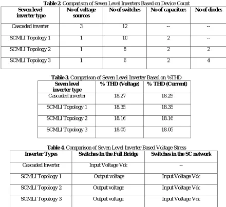
Table 2. Comparison of Seven Level Inverters Based on Device Count
Seven level inverter type
No of voltage sources
No of switches No of capacitors No of diodes
Cascaded inverter 3 12 -- -- SCMLI Topology 1 1 10 2 -- SCMLI Topology 2 1 8 2 2 SCMLI Topology 3 1 6 2 4
Table 3. Comparison of Seven Level Inverter Based on %THD
Seven level inverter type
% THD (Voltage) % THD (Current)
Cascaded inverter 18.27 18.29 SCMLI Topology 1 18.35 18.35 SCMLI Topology 2 18.16 18.16 SCMLI Topology 3 18.05 18.05
Table 4. Comparison of Seven Level Inverter Based Voltage Stress
Inverter Types Switches In the Full Bridge Switches in the SC network
Cascaded Inverter Input Voltage Vdc --
SCMLI Topology 1 Output voltage Input Voltage Vdc SCMLI Topology 2 Output voltage Input Voltage Vdc SCMLI Topology 3 Output voltage Input Voltage Vdc
Comparative study of above four boost inverter is compared on the basis of device count and THD Spectrum. Three comparisons are presented. Table 2 is performed with the number of devices used in those particular circuits. But Table 3 listed the values of percentage of Total harmonic Distortion in the output voltage and output current. Voltage stresses across each switches of four above multilevel inverters are listed in Table 4.
From the analysis cascaded seven level inverter consists of more switching devices and higher %THD is for Switched Capacitor Seven Level Inverter Topology 1, compared to others.
VII. CONCLUSIONS
decreases considerably. Cascaded inverter generates boosted output but it requires separate dc sources. But in Switched Capacitor MLI gives higher output using voltage balancing capacitors. Output of the inverter topologies gives 15 V as amplitude from an input of 5V. So the problem with the circuit having boost converter at the input side or a transformer at the output side can be reduced. From the comparative study, the Total Harmonic Distortion was seen to be reduced for Switched Capacitor MLI Topologies.
ACKNOWLEDGEMENT
Fore mostly, I would like to express my sincere gratitude to our Principal Dr. Soosan George T and HOD Prof. Elizabeth Sebastian for imparting fundamental idea, which helped me a lot for my project. I express my deep sense of gratitude to Prof. Beena M Varghese, for the valuable guidance as well as timely advice which helped me a lot in completing the paper successfully.
REFERENCES
[1] K.W.E. Cheng, “A Step-Up Switched-Capacitor Multilevel Inverter with Self Voltage Balancing”, IEEE Transactions On Industrial Electronics , 2013.
[2]Amrita Mariam Varghese, Beena M Varghese, Elizabeth Sebastian, “FPGA based Single Phase Switched Capacitor Boost Multilevel Inverter”, IJSRD - International Journal for Scientific Research & Development, Vol. 3, Issue 07, 2015 | ISSN (online): 2321-0613.
[3] Fahmida Iqbal , Masarath Unnisa, “Multilevel Inverter With A Step-up Switched-capacitor & Self Voltage Balancing ”, International Journal of Science, Engineering and Technology Research (IJSETR), Volume 4, Issue 11, November 2015.
[4] Elyas Zamiri, Reza Barzegarkhoo, “A Hybrid Switched-Capacitor Multilevel Inverter with Self Charge Balancing and Less Number of Switches”, The 6th International Power Electronics Drive Systems and Technologies Conference, February 2015.
[5] Elyas Zamiri, Naser Vosoughi, “A New Cascaded Switched-Capacitor Multilevel Inverter Based on Improved Series-Parallel Conversion with Less Number of Components”, IEEE Transactions On Industrial Electronics , 2015.
[6] Jos Rodrguez, Jih-Sheng Lai and Fang Zheng Peng, “Multilevel Inverters: A Survey of Topologies, Controls, and Applications”, IEEE transaction on industrial electronics Vol. 49, No. 4, August 2002.
[7] Akira Nabae, Isao Takashi, “A New Neutral-Point-Clamped PWM Inverter”, IEEE transaction on industrial applications, Vol. IA-17, No. 5. September/October 1981.
[8] “A New Boost Switched Capacitor Multilevel Inverter Using Different Multi Carrier PWM Techniques”, International Conference on Circuit,
Power and Computing Technologies, 2014.
[9] S.S. Deshmukh, “Effective Loss Reduction Analysis in New Switched- Capacitor Boost-Multilevel Inverter Using Series/Parallel Conversion”, IEEE Students Conference on Electrical, Electronics and Computer Science, 2014.