University of South Carolina
Scholar Commons
Theses and Dissertations
2018
Structurally Integrated Reconfigurable Wideband
Array For Conformal Applications
Michael Damon Wright
University of South Carolina
Follow this and additional works at:https://scholarcommons.sc.edu/etd Part of theElectrical and Computer Engineering Commons
This Open Access Dissertation is brought to you by Scholar Commons. It has been accepted for inclusion in Theses and Dissertations by an authorized administrator of Scholar Commons. For more information, please [email protected].
Recommended Citation
S
TRUCTURALLYI
NTEGRATEDR
ECONFIGURABLEW
IDEBANDA
RRAY FORC
ONFORMALA
PPLICATIONS byMichael Damon Wright
Bachelor of Science
University of South Carolina, 2013
Submitted in Partial Fulfillment of the Requirements
For the Degree of Doctor of Philosophy in
Electrical Engineering
College of Engineering and Computing
University of South Carolina
2018
Accepted by:
Mohammod Ali, Major Professor
Grigory Simin, Committee Member
Guoan Wang, Committee Member
Juan Caicedo, Committee Member
ii
iii
DEDICATION
I am going to dedicate this dissertation to my cat, Bussy. Mostl y
because I can, but also for all of her help and for being fluffy and not very
iv
ACKNOWLEGEMENTS
Professor Ali obviously deserves acknowledgment for dealing with
contracts, grant expirations, equipment loans, leaking ceilings, monthly reports
to contracting companies who likely will neither read nor understand even if
they do read them, and in general dealing with ridiculous amounts of
government and university bureaucratic nonsense that allowed me to slowl y
chip away at this work with relatively few distractions.
The gentlemen at the multifunctional structures group at the AFRL also
deserve recognition. Mr. Dave Zeppettella for defending our project to
management who were not always the most receptive of the CLAS idea. Mr.
Jason Miller for diligently working on everything we requested of him, even
though some ideas prove brighter than others.
I would also like to thank Evonik Foams, Inc. for their generous samples
v
ABSTRACT
Structurally integrated conformal antennas offer significant advantages
over traditional bolt on antennas , especially for air vehicle applications. The
ability to leverage the entire structure allows for unconventionally large
antennas and arrays to be implemented in a manner which does not detract from
the aerodynamic, structural or aesthetic qualities of the vehicle. Works along
this line have included Slotted Waveguide Antenna Stiffened Structures
(SWASS), conformal helix and spiral antennas, Log Perio dic Dipole Arrays
(LPDA), and other antennas.
An area which has not been investigated to date is the possibility of
implementing reconfigurable antennas in a structural environment. There are
inherent challenges with this approach including the performanc e of electronic
switches when embedded in structural epoxy, the use of non -standard
substrates on RF performance, process challenges brought about by using
uncommonly large substrates with severe temperature restrictions as antenna
substrates, and the use of additively manufactured conducting traces as a
surface for MEMS instrumentation. These challenges or bott lenecks are
addressed in detail in this dissertation.
This dissertation presents the ideas and methods associated with creating
structurally embedded frequency reconfigurable aperture coupled patch
vi
reconfigurable wideband pixelated patch antenna for 1 -2 GHz frequency range
is presented. This antenna demonstrates 41% band width with 7.2 dB peak gain
on one tenth of a wavelength thick structure at 1.8GHz. A similar MEMS
reconfigurable 1-2GHz antenna using additively manufactured conducting
traces on structural laminates is presented next. Measured results demonstrate
nearly 41% bandwidth with 7.8dB peak gain. A 4 -band varactor diode
reconfigurable pixel patch antenna with 54% bandwidth and 7.5dB peak gain
is designed for use in a conformal phased array. Finally, a 6 -element, 4-band
varactor reconfigurable phased array ant enna is presented. The 5ft long arra y
contains 1080 varactor diodes and numerous ultra -thin graphite fibers.
Measured results demonstrate array performance from 400 -720MHz with a
peak gain value above 13dB. The array successfully demonstrates broadside
vii
PREFACE
viii
TABLE OF CONTENTS
Dedication ... iii
Acknowledgements ... iv
Abstract ... v
Preface ... vii
List of Tables ... ix
List of Figures ... x
Chapter 1 Introduction ... 1
Chapter 2 L-Band MEMS Reconfigurable Pixel Patch Antenna ... 9
Chapter 3 MEMS Reconfigurable L-Band Patch Antenna in a Structural Sandwich Coupon with Direct Written Conducting Traces ... 71
Chapter 4 UHF Four Band Varactor Reconfigurable Pixel Patch Antenna ... 85
Chapter 5 UHF Varactor Reconfigurable Phased Array Antenna ... 101
Chapter 6 Conclusions ... 141
ix
LIST OF TABLES
Table 2.1 Reconfiguration States of Pixel Patch Antenna ... 16
Table 2.2 Voltage Data from First Structural Coupon ... 39
Table 2.3 Approximate Resistance Values for the Graphite Bias Lines ... 56
Table 2.4 Simulated Electric Field Magnitudes in DC Bias Wires ... 56
Table 4.1 Varactor Diode Electrical Parameters ... 88
Table 4.2 Reconfiguration States of UHF Pixel Patch Antenna ... 97
Table 5.1 Predicted Performance Metrics of Proposed Array ... 113
Table 5.2 Calculated Delay Values for 70mm Line Sections ... 115
Table 5.3 Simulated Results from Phase Shifter... 116
Table 5.4 Simulated Gain and -3dB Beamwidth of Complete Model ... 127
Table 5.5 Measured Delays from Phase Shifter ... 134
x
LIST OF FIGURES
Figure 2.1 Proposed antenna coupon ... 11
Figure 2.2 Alignment of the radiating slot to the feedline and pixel with DC bias wiring shown in red ... 12
Figure 2.3 Groundplane substrate trace dimensions in millimeters ... 12
Figure 2.4 Pixel patch substrate trace dimensions (in millimeters) ... 13
Figure 2.5 The three reconfiguration states for the pixel patch and feedline with active pixels shown in green and inactive regions shown in black ... 14
Figure 2.6 The RF MEMS switch and mounting method ... 17
Figure 2.7 Photographs of the etched transmission line specimens ... 20
Figure 2.8 Measured data from the etched transmission line specimens ... 21
Figure 2.9 Photographs of the First Non−Structural Antenna ... 23
Figure 2.10 Locations of the 8 RF MEMS missing from the First Non−Structural Antenna ... 24
Figure 2.11 Measured S11 from First Non−Structural Antenna ... 24
Figure 2.12 Measured gain from the First Non−Structural Antenna ... 25
Figure 2.13 Measured radiation patterns from the First Non−Structural Coupon ... 26
Figure 2.14 Photographs of the First Structural Coupon ... 27
Figure 2.15 Location of RF MEMS missing on the First Structural Coupon ... 29
Figure 2.16 Measured S11 for the First Structural Coupon ... 30
Figure 2.17 Measured radiation patterns from the First Structural Coupon ... 31
Figure 2.18 Measured gain and efficiency from the First Structural Coupon ... 31
xi
Figure 2.20 Graphical representations showing the correct amount of conductive epoxy to
use during MEMS instrumentation ... 42
Figure 2.21 Images of conductive epoxy on the MEMS contacts ... 42
Figure 2.22 Photographs of the Second Structural Coupon ... 44
Figure 2.23 Measured S11 from the Second Structural Coupon ... 45
Figure 2.24 Measured gain and efficiency data for the Second Structural Coupon ... 46
Figure 2.25 Measured radiation patterns from the Second Structural Coupon ... 46
Figure 2.26 Simulated S11 measurements showing the effect of DC bias wires on the antenna ... 49
Figure 2.27 Simulated electric field distributions for the pixel patch and DC busbar traces without the introduction of DC bias wiring ... 50
Figure 2.28 Simulated electric field distributions for the pixel patch after the introduction of DC bias wiring ... 51
Figure 2.29 Layout of the DC bias lines redesigned as graphite meander traces (in millimeters) ... 55
Figure 2.30 Simulated S11 plots comparing the model before the introduction of DC bias wires (No Wires), after DC bias wiring was included (Wires), and after the conversion to High-impedance graphite bias lines (Graphite) ... 57
Figure 2.31 Simulated electric field distributions with graphite bias lines ... 58
Figure 2.32 Layout of the sawtooth shaped graphite lines (in millimeters) ... 59
Figure 2.33 Simulated S11 from the pixelated patch antenna with high-impedance sawtooth shaped graphite bias lines ... 61
Figure 2.34 Simulated electric field magnitudes from the pixelated patch antenna with high-impedance sawtooth shaped graphite bias lines ... 62
Figure 2.35 Photographs of the Sawtooth Graphite Pseudo Coupon ... 63
Figure 2.36 Measured S11 from the Sawtooth Graphite Pseudo Coupon ... 65
Figure 2.37 Measured gain and efficiency results from the Sawtooth Graphite Pseudo Coupon ... 66
xii
Figure 3.1 Optical profileometer scans of the surface of the Mesoscribe deposited conducting traces before and after smoothening. All images taken at the same μm scale ... 77
Figure 3.2 Experimental results of the sanded and gold plated Mesoscribe transmission line specimens ... 79
Figure 3.3 Magnified images of sections of graphite fibers under the pixel patch antenna ... 81
Figure 3.4 Photographs of the fully structural pixel patch antenna with additively manufactured traces ... 82
Figure 3.5 Measured results from the fully structural pixel patch antenna with additively manufactured conducting traces ... 82
Figure 3.6 Measured radiation patterns from the fully structural pixel patch antenna with additively manufactured conducting traces ... 83
Figure 4.1 Package dimensions of the Skyworks 1265 varactor diode in millimeters ... 87
Figure 4.2 Illustrations of the pixel patch biasing scheme and varactor diode schematics ... 88
Figure 4.3 Illustrations of the different diode configurations simulated in HFSS ... 90
Figure 4.4 Simulation results of switches created out of the diode configurations of Fig. 4.3 ... 90
Figure 4.5 Transmission line specimens with the varactor diode switching element ... 92
Figure 4.6 Measured S21 data from the measured transmission line specimens compared to simulated projections ... 92
Figure 4.7 Sequence of converting a basic aperture coupled patch to the varactor reconfigurable pixelated patch antenna using 140×200mm patch, 120×20mm slot, 18mm stub, and 50mm core ... 94
Figure 4.8 Simulated S11 results showing the effect of converting the aperture coupled element to a pixelated antenna. ... 95
Figure 4.9 Layout and configurations of the 4−band varactor reconfigurable UHF pixel patch ... 96
Figure 4.10. DC biasing used in the simulation model for the UHF pixel patch ... 98
xiii
Figure 4.12 Simulated radiation patterns from the UHF 4−band varactor reconfigurable pixel patch antenna ... 100
Figure 5.1 Simulation model for evaluating mutual coupling between two EHB and two LB antenna elements ... 107
Figure 5.2 Simulation results showing mutual coupling between two elements based on variation in element spacing ... 108
Figure 5.3 Simulation results showing S11 response of an element based on proximity to a second element based on variation in spacing ... 108
Figure 5.4 Normalized plots of the array factor for the proposed array plotted over 0 ≤ θ ≤
π for selected frequencies. θ0 = 90° indicates broadside, θ0 = 55° indicated 35° beam steering... 112
Figure 5.5 Simulation model of the designed phase shifter. Dimensions of substrate are 103.27mm by 426mm ... 116
Figure 5.6 Simulation results from the phase shifter of Fig. 5.5 ... 116
Figure 5.7 Simplified simulation model of the proposed array. Dimensions in
millimeters. ... 119
Figure 5.8 Simulated S11 results from the simplified 6−element varactor reconfigurable array ... 119
Figure 5.9 Simulated mutual coupling between antenna elements from the simplified 6−element varactor reconfigurable array ... 120
Figure 5.10 Simulated realized gain patterns from the simplified 6−element varactor reconfigurable array ... 120
Figure 5.11 Layout of the DC bias lines (in blue) and DC power connections for the proposed array with the width of the bias lines exaggerated for clarity... 124
Figure 5.12 Simulated S11 results from the complete 6−element varactor reconfigurable array with DC bias and superstrate ... 125
Figure 5.13 Simulated mutual coupling between antenna elements from the complete 6−element varactor reconfigurable array with DC bias and superstrate ... 126
Figure 5.14 Simulated realized gain patterns from the complete 6−element varactor reconfigurable array with DC bias and superstrate ... 126
xiv
Figure 5.16 Measured S11 results from the six antenna elements before integration into an
array ... 132
Figure 5.17 Photograph of phase shifter with copper tape shorted delay lines ... 133
Figure 5.18 Measured results from the presented phase shifter... 134
Figure 5.19 Photographs of the UHF varactor reconfigurable array ... 135
Figure 5.20 Measured S11 results of the array elements as they appear in the presence of the array ... 136
Figure 5.21 Measured S−parameter results from the 4−band varactor reconfigurable array ... 137
Figure 5.22 Measured gain versus frequency plots for the 4−band varactor reconfigurable array with solid line being gain as measured by the Satimo, dashed line being gain minus the losses from the cables and coupler, dotted line directivity ... 137
1
CHAPTER 1
INTRODUCTION
1.1
Motivation
Antennas which possess the characteristics of being conformal,
wideband, and highly directional are of significant interest to both the
commercial and defense industries due to the benefits they provide. The
widespread use of unmanned aerial vehic les (UAVs) for a variety of civil and
defense related tasks magnifies the desire for high -gain antennas suitable for
communications and radar related roles. However, due to the limited payload
capacity in aircraft and smaller UAV’s in particular, such ant ennas must add
minimal weight and drag to the vehicle while retaining the bandwidth and gain
performance which made the antenna attractive originally. This dissertation
undertakes the challenge of designing a highly directional and wideband array
antenna which is electrically efficient and aerodynamically invisible. The
aperture coupled microstrip patch ant enna will be used as the base element for
the array design. To achieve wideband and directional antenna performance
from the microstrip patch antenna, two main research areas will be utilized:
pixelated antennas, and electronic frequency reconfiguration. Additionally,
the array should add negligible weight to a structure along with not degrading
2
designed around non-standard dielectric substrates and materials and employ
the concept of conformal load-bearing antenna structures (CLAS). The
conceptual platform designed for is a large, composite skin UAV with 10’s
sq−ft of relatively planar surface area available for the design to occupy. This
consideration dictates that any fa brication techniques used be translatable to
unconventionally large substrates making many of the traditional antenna
fabrication techniques, such as photochemical etching, significantly more
challenging or altogether unfeasible. Finally, once an antenna design has been
developed which satisfies the above guidelines, the design will be expanded so
that the developed antenna forms the element in a wideband, conformal beam
steering array which will offer superior gain and bandwidth on a low-profile.
Microstrip patch antennas are widely employed due to their low profile
and high directivity. However, a fundamental limitation of the microstrip
patch antenna is the inherently narrow impedance bandwidth which is typicall y
in the vicinity of 3%. Research seeking to increase the bandwidth of the patch
antenna yielded the aperture coupled patch antenna [1-5], including stacked
patch designs which can have bandwidths greater than 50%. Aperture coupled
patch antennas maintain the high directivit y quality of microstr ip patch
antennas, and are well known to greatly increase the impedance bandwidth of
the antenna. The tradeoff for increasing the bandwidth is increased thickness
for the structure, which in some cases can be 0.2λ where λ is the free-space
3
The goal of achieving wideband performance from a microstrip patch
antenna while minimizing its thickness is an area of ongoing investigation [6
-10]. A popular method of achieving a lower profile structure while retaining
high gain performance is to incorporate “U” or “E” shaped slots o n the patch
[11-18], for which a total thickness of approximately λ/10 is typical. The
consequence of imposing the thickness constraint, even in the presence of the
“U” or “E” slots, is a reduction in bandwidth under what would be possible
with a thicker structure. It remains a challenge to maximize both gain and
bandwidth while minimizing thickness for the microstrip patch antenna.
A concept that demonstrates a patch antenna with good gain and
bandwidth with a relatively thin profile is presented in [11]. This paper details
an E-shaped patch antenna with two parallel slots in the patch. This design
achieves a 30.3% bandwidth with a peak gain of approximately 8dB on a 15mm
thick structure for operation between 1.8 -2.5 GHz.
Antennas that utilize electronically controllable switches to reconfigure
with respect to frequency, pattern and polarization etc. have been widely
researched with applications in multiple fields [19 -42]. Of particular interest
are pixelated antennas [19, 43-46], for which the antenna geometry is divided
into multiple subwavelength dimension segments, or pixels. These pixels are
then either connected or disconnected using switches, bringing about the
possibilit y of altering the size and shape of the a perture on demand. A common
choice of switch used is the PIN diode [20 -23, 25-34, 37-39, 41, 43], but
4
demonstrated as well [24, 36, 40, 42]. PIN diodes demonstrate reasonable
isolation and transmission loss at frequencies spanning the L -band and below.
However, PIN diodes are current controlled devices with a biasing circuit
which will dissipate power in the various components. Varactor diodes do not
suffer the disadvantage of requiring a power dissipating DC bias circuit, as a
varactor diode is a voltage controlled device with negligible current draw. The
drawback to varactor diodes is the inherent capacitance ratio of the device
which will begin to limit the isolation and transmission loss performance as
the operating bandwidth becomes wider.
A third choice of electronically controlled switch which has grown in
popularit y in recent years is the micro electro -mechanical switch (MEMS) [44,
47-53]. MEMS can provide insertion loss and i solation performance
comparable to or exceeding what a PIN diode is capable of, and maintain that
performance at much higher frequencies than the PIN diode. Additionally,
MEMS are voltage controlled devices , and similar to a varactor diode, MEMS
require the DC power supply to source nearly zero current. A significant
drawback to implementing MEMS in a design is the question of reliability.
Due to the device containing moving parts which in some cases come into
physical contact with each other, MEMS have a host of failure mechanisms not
present in either PIN diodes or varactor diodes [54 -57]. Additionally, MEMS
are commonly monolithically integrated directly onto the antenna traces [44,
47-48, 50-51, 53]. While convenient for smaller specimens, monolithi c
5
cost involved with attempting to microfabricate MEMS on a 10’s of sq -ft large
area of aircraft skin laminate would be prohibitive, if the fabrication was even
technically feasible to begin with.
An alternative to monolithic fabrication of MEMS devices was made
commercially available by Radant MEMS, Inc. in the form of an individuall y
hermetically sealed package, cantilever beam MEMS chip [58]. The Radant
series of MEMS devices claim low insertion loss (0.24dB @ 2.4 GHz) and high
isolation (27 dB @ 2.4 GHz) with a long lifetime (> 100 billion cycles @
30dBm). These devices have been successfully demonstrated to work for
reconfigurable antenna designs [49, 52] as well as a 25,000 MEMS device
electronically steerable antenna array [59]. The Radant chip opens the
possibilit y for us to integrate a MEMS device with our designs without needing
to microfabricate devices on unconventionally large substrates.
Conformal Load Bearing Antenna Structure (CLAS) [60-61] concepts
merge the antenna with its surrounding structural environment resulting in a
single article which fulfills the loadbearing requirements of the structure while
also providing the radiation property requirements of the mi ssion. This concept
provides a solution with significantly reduced weight and drag values over
conventional parasitic antenna integration schemes. The integration efficiency
of CLAS enables an air vehicle to host unconventionally large antenna leading
to increased antenna performance potential. However, the CLAS concept of
antenna design does not allow for Rogers or other low loss Teflon based
6
suitability for structural bonding and its lack of structural stiffness . The
antenna substrates are therefore limited to fiberglass, Kevlar, or other materials
which are suitable for use in fabricating structural panels.
1.2
Contributions
This dissertation presents a pixelated, MEMS frequency reconfigurable,
conformal, wideband patch antenna for L-band; a fully structural MEMS
frequency reconfigurable, conformal, wideband patch antenna for L -band with
additively manufactured conducting traces; a varactor diode frequenc y
reconfigurable, conformal, wideband CLAS patch antenna for UHF; a UHF
array antenna with the UHF pixel patch as the base element suitable for
structural integration. Both the L-band and UHF designs proposed here are
designed and fabricated as part of a structural material environm ent and have
wide ranging applications, such as radar, cognitive radio communications, and
satellite communications.
The first contribution is the MEMS frequency reconfigurable conformal
wideband pixel patch antenna for CLAS which functions in the 1 -2 GHz
frequency range. To the best of our knowledge, the patch antenna element
achieves an unprecedented combination of gain and bandwidth for a patch
antenna of similar electrical thickness. Additionally, novel fabrication
techniques were developed to enable a low-cost fabrication procedure s which
do not require specialized micro -fabrication facilities. The patch antenna
7
transmission line feed. Both the patch and the feedline are frequenc y
reconfigurable to three distinct states through the use of MEMS. These three
reconfiguration states correspond to three separate but overlapping frequenc y
bands which cover a range of frequencies much wider than what is typically
possible for a patch ante nna without allowing the thickness of the coupon to
grow. Measured impedance and gain data are presented for a fully functioning
protot ype pixel patch antenna with MEMS installed.
The second contribution builds on the L−band MEMS reconfigurable
pixel patch antenna by demonstrating a fully functioning structurall y
integrated antenna with additively manufactured conducting traces. The
resulting specimen is the embodiment of the CLAS concept, with no portion of
the fabrication unable to be applied to unconventionally large and curved
surfaces. Measured impedance and radiation pattern data with functioning
MEMS are presented and show a marked improvement over previous
specimens.
The third contribution is a varactor diode reconfigurable, conformal and
wideband patch antenna functioning in the UHF band and suitable for CLAS.
This design is similar to that of the L-band patch antenna, except with the scale
of the geometry, switching device, and the DC biasing scheme altered resulting
in an even greater percent bandwidth. The UHF pixel patch element functions
in the 400-800 MHz range with four separate but overlapping frequency bands
8
along with measured impedance data for multiple experimental specimens are
presented.
The final contribution is a conformal, wideband scanning phased arra y
incorporating the varactor reconfigurable UHF pixel pat ch. Simulated results
detailing the design procedure for the array are presented, followed by a full y
functioning six element experimental specimen with over one thousand
varactor diodes. Measured results including gain and radiation pattern data are
presented and show a wideband phased array on an electrically thin coupon
with 35° beam steering capability in reasonable agreement with simulation
9
CHAPTER 2
L-BAND MEMS RECONFIGURABLE PIXEL PATCH ANTENNA
2.1
Introduction
As indicated, the first focus of this work is on developing RF MEMS
reconfigurable, directional , and conformal patch antennas which are fully
integrated as part of a structural environment. Traditionally, antenna
researchers favor substrates such as Duroid 5880 or R O4003 over fiberglass
substrates (FR4) due to their superior homogeneity and lower loss
characteristics. Considering a structural environment however, these materials
are not suitable; both from the difficulty associated with bonding other
materials to that material as well as the lack of structural stiffness that is
required from materials that are to be used in fabricating a structure. Neither
are the conventional methods of integrating RF MEMS devices and passives
(wire bonding, soldering etc.) suitabl e for a structural environment. The
complication and cost associated with wire -bonding on an unconventionally
large substrate would prove prohibitive if the fabrication was at all feasible.
Additionally, there exist concerns from a structural application viewpoint as
to the durability of the bond wires used in the wire -bonding process when
10
Our work uses FR4 substrates rather than the more RF favorable
materials. FR4 serves as a reasonable e lectrical approximation of the structural
fiberglass laminates which are used to create structural coupons. We also use
the layers of structural epoxy and structural foam core material which are
required for the bonding process. Our own laboratory measur ements have
shown that FR4 and fiberglass (E -glass epoxy) have the same dielectric
constant (4.4) and loss tangent (0.02). Since FR4 is readily available with
copper on both sides and is easy and low cost to etch and gold plate it was
selected to fabricate our antenna. Notwithstanding that the same antenna and
all its feed and DC bias traces can be fabricated on structural fiberglass
laminates using additive manufacturing techniques such as deposition of
conductors using plasma spray. Such techniques have b een shown to deposit
conductors as thick as 100 microns and be suitable for gold plating afterwards
to prevent corrosion. To avoid the high cost associated with such fabrication
we chose to use copper-clad FR4 instead.
Also in this work, the RF MEMS device s will be installed using an
unconventional inverted-chip method where electrical connections will be
established using conductive epoxy which eliminates the need for ultra -thin
(1-2 mil diameter) bond-wires.
2.2
Antenna Configuration, Materials and Fabrication
The proposed reconfigurable pixelated antenna requires three substrates.
11
Mold Line) for the structure. However, for the purpose of this work the OML
material will not be studied and built. The interested readers can consult our
previous work on that [63].
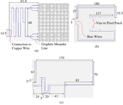
Fig. 2.1 illustrates the antenna stackup. Fig. 2.2(b) shows the antenna
structure with the DC bias wire routing shown in red. Fig. 2.2(a) is an overla y
showing the alignment of the different features of the antenna. The firs t
substrate from the bottom of the antenna is a 1.6mm thick FR4 (𝜀𝑟=4.4,
tan𝛿=0.02) panel with details shown in Fig. 2.3. The bottom side of this
substrate contains a microstrip feedline, two RF MEMS switches, three 40kΩ
DC bias resistors, and associated DC bias traces to provide 90V and ground
connection for the RF MEMS, and two tuning stubs. The upper surface of this
substrate contains the antenna ground plane with a 45mm by 4.5mm coupling
slot which is centered at the center of the ground plane substrate. The ground
plane is solid copper and spans the entirety of the antenna except in the area Ground Plane
Substrate Radiating Patch
Patch Substrate
DC Busbars
Foam Core
Ground Plane
Microstrip Feedline
12
left for the slot. The antenna will be excited through an end -launch SMA
connector feeding the 50Ω microstrip feedline which is located on this
substrate.
The second substrate is the foam core which maintains the separation
between the ground plane and the patch substrate. The foam core is 17mm
Figure 2.2 Alignment of the radiating slot to the feedline and pixel with DC bias wiring shown in red: (a) top down view showing all layers with the connection points for the DC bias wires annotated in red, (b) side view of antenna.
DC Bias Wire Connection Points
(b) (a)
Figure 2.3 Ground plane substrate trace dimensions in millimeters: (a) Upper surface of substrate with ground plane and radiating cavity, (b) underside of substrate with feedline, (c) area of feedline showing the reconfigurable stubs and DC bias traces.
(b) (a)
45
4.5
Bias Wire Via Holes
(c)
Ground Connection Lowband
Stub
MEMS Pockets MEMS Gate Pads Midband
Stub
13
thick Rohacell WF 51 (𝜀𝑟=1.06, tan𝛿=0.0003) structural, closed cell foam. The
foam fills temperature and compression rating requirements brought about by
the need to autoclave cure the structural specimen. The foam core is bounded
on the upper and lower surface by thin (1 -2 mil) layers of structural epoxy
which adheres the foam core to the ground plane and patch substrates. Our
simulation analysis neglects to include these layers of structural epoxy due to
their very small thickness.
Above the foam core is the third substrate, termed the Patch Substrate
which is shown in Fig. 2.4.
This panel is 0.4mm thick FR4 (𝜀𝑟=4.4, tan𝛿=0.02). The upper surface of the
Patch Substrate contains the pixelated patch antenna traces, thirty-six MEMS,
five 40kΩ DC bias resistors, gate pad traces to provide 90V to the MEMS, and
two ground pads. The lower surface of this substrate contains four DC busbars
used for supplying 90V to the gate pad traces, as well as one DC ground busbar
Figure. 2.4 Pixel patch substrate trace dimensions (in millimeters): (a) Upper surface of substrate with pixel patch traces, (b) underside of substrate with DC busbars, (c) area of pixel patch showing traces in the vicinity of the MEMS pocket, (d) view of MEMS chip resting in pocket.
(c)
(a) (b)
DC Bias Wire Connection Points
Gr
ound P
ad
MEMS Gate Pad
14
which connects the two ground pads. The pixel patch is centered at the same
location on the horizontal plane as the coupling slot.
Frequency reconfiguration will oc cur through altering the length of the
pixel patch and feedline to achieve multiple distinct but overlapping frequency
bands (see Fig. 2.5).
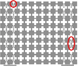
The pixelated patch is 𝑛 conductive pixels along the width, and 𝑚 conductive
pixels along the length. For this work we consider 𝑚=11 and 𝑛=9. Also, for
this work the pixels are 5mm square and separated on all sides by 2.5mm. The
inner 9×7 pixels are all permanently connected to each other by 1mm wide
bridges which span the 2.5mm gap between pixels. Observing Fig. 2.5, it can
be seen that the rows labeled Row 1−4 are not connected to the inner 9×7 grid
Figure 2.5 The three reconfiguration states for the pixel patch and feedline with active pixels shown in green and inactive regions shown in black: (a) Highband, (b) Midband, (c) Lowband.
(a) (b) (c)
Row 1
Row 2
15
of pixels. These four rows contain the reconfigurable elements of the pixel
patch and are connected to the central section of pixels through RF MEMS
switches. Rows 1 and 2 are referred to as the two inner rows and are required
to achieve both the Midband and Lowband reconfiguration states. Rows 3 and
4 are referred to as the two outer rows and are required for th e Lowband state
only. Each pixel along the width of rows 1 and 2 is connected to the adjacent
pixel in the central 9×7 section of pixels through one RF MEMS switch.
Similarly, each pixel along the width of rows 3 and 4 is connected to the
adjacent pixel of rows 1 and 2 through one MEMS switch. Thus, four rows of
MEMS, each with 9 MEMS in a row, make up the complement of 36 MEMS
present on the pixel patch substrate.
The microstrip feedline contains two tuning stubs in addition to the base
stub provided from the feedline. These stubs perform an important function of
impedance tuning the antenna at its respective band. Each frequency band for
the pixel patch antenna has a corresponding configuration for the feedline
which must be present for the antenna to be properly impedance matched. Two
RF MEMS switches connect the two tuning stubs with the microstrip line. The
Highband frequency band requires all RF MEMS to be in the OFF state.
Closing the switch that connects the feedline to the first tuning stub h elps to
match the Midband configuration. Closing both RF MEMS switches
simultaneously helps to match the Lowband. The dimensions of the different
patch configurations with expected operating frequencies are shown in Table
16
As mentioned previously, the typical method of gold plating the antenna
traces and wire bonding the MEMS in place was found to be unfeasible due to
concerns over the physical durability of the wire bonds and difficulties
anticipated with wire-bonding structural panels. Equally unfeasible is the
possibility of monolithically integrating RF MEMS switches onto our antenna
traces for similar reasons which make wire bonding unsuitable. We chose a
solution to this quandary in the form of a commercially available RF MEMS
switch in a hermetically se aled packaged chip from the Radant MEMS company
(model RMSW101). Using this device, we developed a completely non
-traditional and innovative method of electrically connecting RF MEMS
switches to antenna traces.
Our method of installing the RF MEMS chips i s based off of the flip
chip method which is well known. However, to our knowledge this method
has never before been applied to a RF MEMS device and presents a new
low-cost option for integrating RF MEMS switches with a design. The general idea
of the method is shown in Fig. 2.6. A small amount of conductive epoxy is
applied directly to the gate, drain, and source contacts of the RMSW101 chip.
The chip is then inverted and placed on the antenna such that the contact pads
Table 2.1. Reconfiguration States of Pixel Patch Antenna
L W L W Stub Length Bandwidth
(Pixels) (Pixels) (mm) (mm) (mm) (GHz)
Highband 7 9 50 65 6.4 1.5−1.9
Midband 9 9 65 65 10 1.4−1.6
17
of the chip rest directly on the appropriate pads of the antenna trace, separated
only by the thin layer of conductive epoxy. The RMSW101 device is intended
by the manufacturer to have the switch ground plane be connected to the RF
ground of the system. However, our meth od neglects this connection and
leaves the ground plane of the chip floating, with no observable detrimental
effects.
There are inherent fabrication challenges to this method of installation.
To place the chip on the antenna trace in an inverted manner, a pocket which
fits the glass case of the RMSW101 must be created in the antenna substrate.
The pocket is a relatively small feature with a length and width measuring
1.2 × 0.8mm. Furthermore, the pocket must be precisely located so that the
contacts of the chip align correctly with the pads of the antenna trace to within
approximately ± 0.1mm. Due to the small feature size and precision required,
it was found that the pocket was best created using an automated router to mill
the pockets in the antenna su bstrate. Even with the aid of an automated router, (a)
Conductive Epoxy Applied to MEMS
Contacts (b)
18
extreme care must be taken to assure proper indexing of the specimen on the
router as even minor misalignments of pockets to antenna traces will render
the specimen unusable. However, regardless of the d ifficulties associated with
creating the pocket, the fact that the chip can be successfully installed without
wire bonding is of paramount importance. This opens up a low-cost option for
integrating RF MEMS switches with a design, which for reasons of siz e or
material, may have been previously unviable.
Voltage is supplied to the RF MEMS through the 4 DC busbars which
are located on the underside of the patch substrate, with one busbar being
connected to each of the RF MEMS devices in the respective row through a
conducting via. Utilizing the busbars in this way allows the entire complement
of 36 RF MEMS to be controlled through a total of 5 DC bias wires attached
to the pixel patch antenna. One wire for each row of RF MEMS, and one
ground wire which is connected to both ground pads through the DC ground
busbar. The connection points and general routing of the DC bias wires can
be seen in Fig. 2.4(a) and (b). Due to being electrically joined by the busbars,
the individual MEMS in any one row cannot be controlled individually. There
is only the ability to control the entirety of a single row individually.
Undoubtedly, if each switch could be controlled independently, more
opportunities for reconfiguration would be possible. However, for this work a
simpler approach was chosen due to other significant issues requiring
investigation before a viable structurally integrated, reconfigurable antenna
19
The DC bias wires are routed straight downward from their connection
point on the pixel patch through the patch substrate, foam core, ground plane,
and ground plane substrate. The wires emerge from the ground plane substrate
at the locations circled in Fig. 2.3(b). The ground wire from the pixel patch
RF MEMS devices is then connected to the ground wire for the feedline RF
MEMS device resulting in one DC ground common for the entire complement
of RF MEMS on both the patch substrate and ground plane substrate. The four
DC voltage wires from the patch are then bundled together with the two DC
voltage wires from the feedline and the antenna DC ground connection and
routed to the edge of the coupon so that they can be connected to a 90V power
supply.
2.3
MEMS Performance
The performance (insertion loss, isolation, return loss) of the MEMS
when the devices are mounted in an inverted manner with electrical
connections made with conductive epoxy is unconventional and is not well
understood compared to their performance when wire bonded (well
documented). To get a clear understanding and comparison w ith wire bonded
MEMS, several transmission line specimens with inverted MEMS switches
were installed using conductive epoxy (EPO−TEK H20E, 𝜌 ≤ 0.0004 Ωcm
from data sheet, cure condition: 120°C for 1 hour). The S11 and S21 data vs
frequency of the MEMS (O N and OFF) were then measured. A dummy
20
determine the insertion loss due to the MEMS and the conductive epoxy. Fig.
2.7(a) shows what is termed the “dummy line.” This is a 50 microstrip
transmission line printed on a section of FR4 with a thickness that matches the
material and thickness of the feedline and ground plane substrate for the
antenna. Fig. 2.7(b) is a second transmission line identical to the dummy line,
except for the inclusion of two MEMS, two DC bias resistors, and four DC bias
wires. The MEMS are mounted using the inverted chip and conductive epoxy
method intended for the pixel patch antenna. The wires used to bias the MEMS
are solid copper. The four bias wi res can be seen in Fig. 2.7(c) and (d).
The insertion loss due to the MEMS was determined by first measuring
the insertion loss for the “dummy line”, and then measuring the insertion loss
for the 2-switch line. The insertion loss for the dummy line was then subtracted
from the 2-switch line insertion loss. This leaves as a remainder the loss due
(a) (b)
(d) (c)
21
to the two MEMS present on t he 2-switch line. The results of the experiment
are shown in Fig. 2.8. The RMSW101 datasheet provides the expectation of
approximately 0.2 dB of insertion loss per MEMS in the 1−2 GHz frequency
range when wire bonded. The insertion loss observed in our measurements is
generally lower than specified in the datasheet, possibly because we have not
used bond wires and made direct connections between the MEMS pads and the
contact pad with a miniscule amount of conductive epoxy. Note that as the
frequency increases to 2 GHz the insertion loss of our method of switch
assembly becomes closer to the wire bonded method. Regardless, the results
of Fig. 2.8 provide evidence that our method o f inverting the MEMS chip and
making electrical connections with conductive epoxy is viable for fabricating
the proposed pixelated patch antenna.
Figure 2.8 Measured data from the etched transmission line specimens: (a) S21 for the Dummy Line, 2 switch line, and MEMS loss, (b) S11 and isolation for the 2 switch line.
22
2.4
Non-Structural Antenna
This antenna is termed the “First Non -Structural Antenna” and was
created using etched FR4 boards (εr ~ 4.4) with 1 oz copper traces. The patch
substrate board measures 81mm x 67mm x 0.4mm and the ground plane
substrate measures 453mm x 178 x 1.6mm. An air gap of approximately 17mm
separates the ground plane substrate from the patch substrate with small foam
spacers used to maintain separation and support the patch substrate. The patch
substrate board is not extremely rigid, and the foam spacers were cut out from
a larger foam body by hand. These two facts mean that the actual separation
between the two substrates is not precisely 17mm, but rather17mm +/ - 1mm.
Photographs of this specimen are shown in Fig. 2.9.
This specimen is configured with a total of 21 DC bias wires attached to
the patch substrate rather than the originally intended 5 wires. One copper
wire is allocated for each gate pad trace on the patch substrate, allowing for
individual control of 16 pairs of MEMS and 4 individual MEMS. There is also
a single ground wire which serves the entirety of the patch. Due to
uncertainties in the fabrication process during this point we experienced a
greater than 50% rate of failure for installing the MEMS due to ESD events,
unsatisfactory pockets, and other various errors during fabrication. The
addition of 1 bias wire for every gate pad trace provi ded a means to more
effectively test the installed MEMS. It was understood that the additional
wires would negatively affect the tuning of the antenna, but the need to
23
necessitated the removal of the positive voltage DC busbars on the underside
of the patch substrate, which was done for this specimen.
The MEMS pockets for this specimen were created by hand. This was
achieved with the use of a drill press, small file, and a small razor knife. The
creation of the pockets using these tools is an imprecise process and led to a
portion of the pockets being unsuitable for MEMS installation. As a result,
this specimen was tested with 8 MEMS missing from the positions shown in
Fig. 2.10.
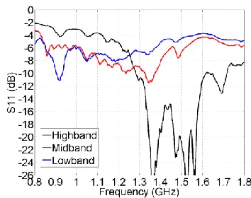
The measured S11 for the First Non -Structural Antenna is shown in Fig.
2.11. Considering a minimum S11 requirement of −10d B, the Highband shows
(a) (b)
(c) (d)
24
a dual band performance rather than the intended wideband response. The
Highband is resonant from approximately 1.46 to 1.48GHz and from 1.60 to
1.67 GHz. At no point does the Midband S11 satisfy the −10dB requirement,
but a resonance below −6dB from 0.95 to 1.12 GHz is present. The Lowband
satisfies the −10dB requirement at 0.94 GHz with approximately 30MHz
bandwidth.
The S11 plot demonstrates frequency reconfiguration, with three
frequency bands being apparent. The most significant reconfiguration occurs
Figure 2.10 Locations of the 8 MEMS missing from the First Non-Structural Antenna.
25
between the Highband and Midband, along with a smaller but still defi nite
reconfiguration between the Midband and Lowband. However, none of the
three bands show impedance matching which meets expectations. The
Midband is required to be shifted higher in frequency to cover the 1.2 to 1.4
GHz range as well as have improved matching. The Lowband reconfigured to
the correct frequency range but is intended to have a bandwidth of
approximately 100 MHz rather than 30MHz.
This antenna was measured in a Satimo anechoic chamber for pattern
and gain within the frequency range of 1 to 2 GHz. Gain and efficiency versus
frequency plots are shown in Fig. 2.14.
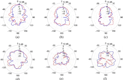
Radiation patterns are shown in Fig. 2.13. The radiation patterns show the E
-plane (red) and H--plane (blue) patterns for the antenna as measured at the
frequency of maximum gain for each band. Fig. 2.13 (a) shows the Highband
at 1.42 GHz, Fig. 2.13(b) the Midband at 1.38GHz, and Fig. 2.13(c) the
Lowband at 1.36 GHz.
(a) (b)
26
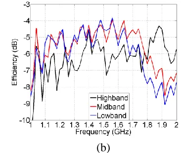
The measured results for the antenna show that even though the S11
demonstrates frequency reconfiguration, the gain is less than desired. This
is because of the poor efficiency shown in Fig. 2.13(b). This antenna was
expected to maintain an efficiency of approximately -2 dB over its operating
bandwidth. However, the m easured results show that the efficiency is worse
than -3 dB for all frequencies with the Lowband being particularly inefficient
with its best efficiency being slightly better th an -8 dB at 1.36 GHz.
Of positive note for this antenna is the observation that although the
efficiency and impedance matching are poor for all frequency bands, each band
still has positive gain as shown in Fig. 2.13(a). At -8 dB efficiency, the
Lowband provides 2 dB of gain. At -3.5 dB efficiency, the Midband provides
5 dB of gain at a point where the S11 magnitude is approximately -5dB. These
observations indicate that if the Lowband efficiency and overall impedance
matching can be improved, the antenna will provide gain magnitudes of
upwards of 5dB across all frequency bands .
(a) (b) (c)
27
Measured S11 data demonstrated frequency reconfiguration in 3 bands,
with all bands showing positive gain values. The Highband and Midband
achieved gain values of 5 dB, while the Lowband achieved above 2dB of gain.
However, none of the reconfiguratio n states demonstrated S11 bandwidth
acceptable to the project goals.
2.5
First Structural Antenna
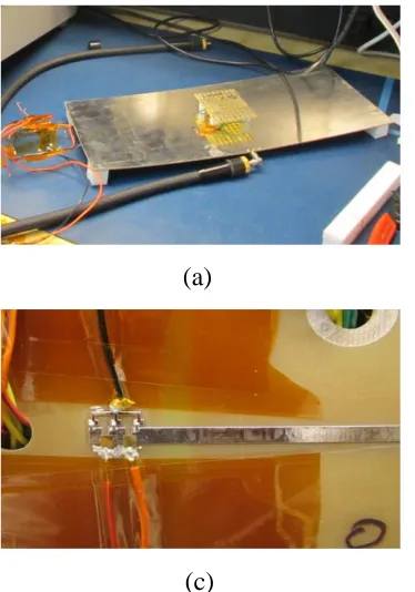
The second antenna fabricated is termed the “First Structural Coupon”
and is shown in Fig. 2.14.
The antenna coupon measures 178 × 470 × 19 mm and is comprised of the
0.4mm thick patch substrate, 17mm thick Rohacell WF 51 (𝜀𝑟= 1.06, tan𝛿 =
0.0003 @ 2.5GHz) foam core, and 1.6mm thick ground plane substrate. There
is also a layer of structural epoxy between the patch substrate and foam core,
and another layer between the foam core and ground plane substrate. This
(a) (b)
28
structural epoxy is of negligible thickness (t~2mil) and is necessary to bond
the individual layers of the structure together into a coupon.
The antenna artwork is identical to that of the previous non -structural
specimen, and once again was etched. The antenna s ubstrates remain FR4
(𝜀𝑟~4.4), however the substrate panels used for this specimen are not of the
same batch as the previous specimen and so may have marginally different
dielectric properties. The ground plane is solid copper and spans the entire
area of the coupon with the exception of where the slot is located.
Originally it was planned for all specimens following the previous non
-structural specimen to use only 5 DC bias wires to control the MEMS as per
the original design. However, the MEMS placem ent techniques were still not
well refined for this specimen, so the decision was made to again control the
MEMS with 21 DC bias wires to aid in troubleshooting. To simplify and reduce
risk to the process of connecting the DC bias wires to the DC power su pply, a
switch board was fabricated to minimize handling of the bias wiring. The
switch board is visible in the figure and consists of 22 mechanical toggle
switches mounted on top of a FR4 board with tr aces running along the
underside. These traces conn ect the toggle switches to a connector on the edge
of the board. The antenna bias wires can then plug into the switch board using
a 25 pin Molex connector. The edge of the switch board opposite the DC bias
wires has connectors for the power supply. The result is that once connected;
only the switch board must be handled to change antenna states, reducing the
29
complications rendered a small number of the pockets unsuitable to MEMS
installation. The locations of the missing MEMS are shown in Fig. 2.15.
The inconsistent separation between the patch substrate and groundplane
substrate that was a concern for the First Non-Structural Antenna was solved
by constructing the antenna on the structural coupon. The high pressures
applied to the coupon during the bonding process eliminated any possibility
for these to be variations in the substrate separation. The t rade-off for this
improvement is that instead of an air gap separating the patch substrate from
groundplane substrate, there is the Rohacell foam core which has a higher loss
tangent and dielectric constant than air and will likely produce a small
frequency shift.
The measured S11 for the First Structural Coupon is shown in Fig.
2.16(a), with Fig. 2.16(b) showing the same data formatted to better
differentiate the 3 reconfiguration states. It is immediately observable that the
S11 improved in both resonance magnitude and bandwidth. The Highband is
below −10dB from approximately 1.7 GHz to 2.05 GHz for a bandwidth of 350
MHz. The Midband is nearly resonant from 1.4−1.7 GHz, with only a small
30
gap in the S11 at 1.53 GHz. Ignoring the deficiency at 1.53 GHz, the Midband
has a −10dB bandwidth of 300 MHz. The Lowband is resonant from 1.04−1.4
GHz, for a bandwidth of nearly 400 MHz.
Taken at face value, these S11 plots would seem to indicate a great
success. However, the measured results show that both the Midband and the
Lowband have very close to a 700 MHz bandwidth at −10 dB. This is clearly
far too optimistic of a result, and it is obvious that these bands are
demonstrating a very large amount of loss. The 350 MHz bandwidth for the
Highband is a more realistic result and provides the expectation that it is
working as intended.
The antenna patterns and gain were m easured inside a Satimo chamber .
These results are shown in Fig. 2.17 and Fig. 2.18 . The radiation patterns of
(a) (b)
31
Fig. 2.17 shows the E-plane (red) and H-plane (blue) patterns for the antenna
as measured at the frequency of maximum gain.
A clear reconfiguration between the Highband and Midband is
observable in both the gain and efficiency plots of Fig. 2.18. The peak gain
for the Highband occurs at 1.9 GHz with a value of 4 dB. The Midband peak
gain occurs lower in frequency at 1.62 GHz with a value of 4 dB. This is a
clear improvement over the previous non -structural coupon for which no
(a) (b) (c)
Figure 2.17 Measured radiation patterns from the First Structural Coupon: (a) Highband at 1.90 GHz with E-plane shown in red, (b) Midband at 1.64 GHz with E-plane shown in red, (c) Lowband at 1.50 GHz with E-plane shown in red. E-plane in red, H-plane in blue for all plots.
(a) (b)
32
reconfiguration was observable in the gain or efficiency plots. However, there
is little evidence present in the gain or efficiency plots to indicate a
reconfiguration between the Midband and Lowband. The Midband is
approximately 1 dB more efficient than the Lowband between 1.66 and 1.76
GHz, but outside of that narrow frequency range the efficiency for the two
bands is nearly identical.
Gain for the Highband is less than desired. It is expected for the
Highband to achieve a peak gain of upwards of 7 dB, with a 5 dB gain
bandwidth of approximately 350 MHz. The Highband for this specimen
achieves only a 4dB peak gain, wi th even the 2 dB gain bandwidth being merely
140 MHz. The Midband peak gain is 1 to 2 dB less than what is expected
which might be attributable to the presence of conducting epoxy used to mount
the switches. However, the Midband only achieves 4 dB of gai n at 2 discrete
points with 0 MHz of bandwidth at 4 dB. From a gain standpoint, the specimen
can only really be said to function from 1.64 to 1.90 GHz where gain values
approach 4 dB. Even in this narrow frequency range, there are frequencies
where the gain decreases to values below 3 dB. The frequencies around 1.78
GHz are an especial problem area for which the gain falls off to almost 0 dB.
While this antenna does provide some improvements over the first non
-structural antenna, it has significant flaws and does not satisfy the objectives.
Of the potential causes of failure present in the “First Non -Structural
33
patch substrate height. The concerns involving the 21 DC bias wires and
reliability of the MEMS still exist in this specimen.
2.6
Discussion on MEMS Placement
The fabrication of both the “Non-Structural Antenna” and the “First
Structural Antenna” specimens suffered from excessively high MEMS failures
during the MEMS instrumentation process. A small fraction of the failures
were due to what are best referred to as accidents. These failures would include
MEMS slipping out of twe ezers and being lost, chipping of the MEMS case
during installation, etc. One or two of these failures are expected during the
construction of a pixelated patch antenna and are considered unfortunate, but
ultimately negligible losses. The vast majority o f MEMS failures were
attributable to either ESD events or incorrect application of conductive epoxy.
These two problems created what at times seemed an insurmountable obstacle,
and it was only after solutions to these problems had been found that further
progress on the project was possible.
A. Electrostatic Discharge Control
The easier of the two problems to solve was the issue of ESD
events damaging the MEMS devices. The “First Non -Structural Antenna” was
created before we completely understood the mea sures needed to safely install
the MEMS using our unorthodox method, and ESD events were the primary
34
resolve the problem of ESD events destroying MEMS, we developed a set of
conditions and equipment that must be satisfied for MEMS instrumentation to
occur.
When ESD events are referred to in this work, they mean specifically
that an electrostatic potential greater than 100V has interacted with the MEMS
and caused the internal cantilever beam to become stuck in the closed position
due to stiction. There are perhaps other aspects of ESD damage possible, but
the problem of stiction was one which was reoccurring and easily identifiable.
This problem is especially troubling due to the design of the pixel patch
antenna. ESD events occur generally through the DC bias wires coming into
close contact with an object which has an electrostatic potential. These wires
are grouped together so that electrical connections can easily be made to the
power supply. However, this grouping of the wires dictates that an ESD event
which affects one DC bias wire will generally affect several wires resulting in
several MEMS being lost to any one ESD event. The problem is exacerbated
further due to the pixels i n a row all being connected. If an ESD event has
occurred damaging at least one MEMS due to stiction, it is possible to identify
the problem with a continuity check. With no voltage supplied to the MEMS,
all MEMS should all be acting as open switches. A continuity check performed
across a row of MEMS should thus fail. If the continuity check does not fail
when there is no voltage being supplied to the MEMS, then an ESD event has
occurred and at least 1 MEMS in that row will have to be replaced.
35
determining that at least 1 MEMS in a row has failed, as any 1 MEMS failing
due to stiction causes the entire row to show as a short circuit. The corrective
action then becomes to begin replacing MEMS in the damaged row one by one,
until a continuity check no longer shows any switches in a row as being closed.
It is not possible to determine which MEMS are damaged and which MEMS
are working. In worst case scenarios, all 9 MEMS in a row require replacing
to break continuity, yet exactly how many and which specific MEMS actuall y
failed cannot be determined.
The following equipment and procedures were used to combat the ESD
problem. All work with MEMS, or on the antenna specimens with MEMS
installed, occurred on a grounded ESD safe surface with personnel grounded
through a wrist strap. An ionizer was positioned approximately 3 feet away
from the work area and directed to continuously create a de -ionizing air flow
onto the work area for all fabrication steps involving MEMS. Additionally, a
grounded ESD safe smock was worn at all times while working with MEMS.
When the specimen needed to be placed in an oven, ESD safe gloves were worn
while transporting the antenna to the oven and no traces or wires were allowed
to contact any object during transport.
Despite the equipment listed above, ESD events were still common, and
it was not until we imposed relative humidity requirements along with the
above equipment that the ESD proble m was solved. Through trial and error,
we found that ESD events were unavoidable at relative humidity of 40% or
36
those humidity conditions. Relative humidity between 40% - 50% made ESD
events far less common; however rare incidents were recorded for this relative
humidity range and working with MEMS for these humidity values was
avoided. At relative humidity values of above 50%, no ESD events were
encountered. However, when possible, relative humidity values between 60%
- 70% were preferred to provide as much of a safety margin as possible.
The combination of equipment and humidity solved the problem of ESD
events. These guidelines were not in place during the fabrication of the “Fi rst
Non-Structural Antenna” specimen, and as a result that specimen suffered
significant MEMS losses due to ESD events causing stiction. During the
construction of the “First Structural Coupon” specimen, these guidelines were
being refined. This specimen suffered some, but far fewer ESD related losses.
For antennas subsequent to the “First Structural Coupon” these ESD
precautions were in place and actively followed. Subsequent antennas
experienced 0 losses to MEMS due to ESD events.
B. Conductive Epoxy Application
The second problem which contributed to MEMS failures is the process
of installing the MEMS using conductive epoxy rather than the typical wire
bonding method. With the ESD problem, while it was more difficult to manage
than we originally anticipated, it was foreseeable that we would encounter the
ESD obstacle and we were prepared to develop a procedure given the available
37
other hand was completely unexpected, creatin g problems which were of
research-halting significance yet difficult to attribute to a cause. It was onl y
through many iterations of destructive testing that the approximate cause of
the problems was identified.
Fig. 2.19 shows the circuit diagram for a si ngle MEMS and the
associated bias circuit.
For our case, VG=90V and RS=RD=40kΩ. One of the advantages to using
MEMS is that MEMS dissipate very close to 0W of power in the biasing circuit.
90V is applied to the gate pad of the MEMS, but since there is no physical
connection within the MEMS device from the gate to either the drain or sou rce
terminals, there is no current flow into the gate terminal from the power supply.
The difference in potential between the gate terminal and the source terminal
creates the electrostatic field within the device. This electrostatic field in turn
applies a force to the internal cantilever beam with a large enough magnitude
to force the cantilever beam into the closed position. Radant MEMS gives the Source
(RF In/Out)
Drain (RF In/Out)
VG
RS RD
Gate MEMS