D
e f e c t s
l u i t h i n
C n R B O N - B R S E D
E
l e c t r o n i c
M
r t e r i r l s
Gliuier Pierre Mar i e Gaudin
T hesis subm itted for th e d e g re e of Doctor of Philosophy
D epartm ent of Electronic and Electrical Engineering
University College
•■■111
University of London
UCL
ProQuest Number: 10015070
All rights reserved
INFORMATION TO ALL USERS
The quality of this reproduction is dependent upon the quality of the copy submitted.
In the unlikely event that the author did not send a complete manuscript and there are missing pages, these will be noted. Also, if material had to be removed,
a note will indicate the deletion.
uest.
ProQuest 10015070
Published by ProQuest LLC(2016). Copyright of the Dissertation is held by the Author.
All rights reserved.
This work is protected against unauthorized copying under Title 17, United States Code. Microform Edition © ProQuest LLC.
ProQuest LLC
789 East Eisenhower Parkway P.O. Box 1346
D efects within Carbon-Based Electronic Materials
R
b s t r h c tThe defect states that exist within chemical vapour deposition (CVD) diamond and poly(p-phenylene vinylene) (PPV) thin films have been investigated using a range of techniques. Thermally stimulated currents (TSC) and charge-based deep level transient spectroscopy (Q-DLTS) are the main techniques used. Q-DLTS has been preferred to the most widely-used capacitance-based deep level transient spectroscopy (C-DLTS) due to the wider range of structures it allows to be investigated.
Defects within Carbon-Based Electronic Materials
R
c k n o u j l e d g e m e n t sI wish to thank first my supervisor, Dr Richard B. Jackman, for making it possible for me to start a Ph. D. in his group, at a time when my future in scientific research was rather uncertain. I first met Richard following a long period of unemployment in France and, although my English was not very good at that time, Richard quickly opened the door of his group for me. I am also grateful to Richard for regular opportunities to attend and present my work at international conferences during the whole period of my Ph. D. studies. These meetings have always been extremely useful, offering many chances to confront ideas with other researchers. Many key arguments in the data analyses presented here have followed such discussions.
London is an expensive place to live in and I could not have completed my Ph. D. without permanent financial support. The award of a post-graduate studentship from Centronic Ltd., Croydon, UK, for the whole period o f my Ph. D. studies is greatly acknowledged. The Semiconductor Physics Group of the Institute of Physics (lOP) and the Graduate School at UCL significantly contributed to the costs of attending the Diamond 2000 Conference in Porto (Portugal) in the form of travel bursaries. The lOP also provided several small grants for attending its Annual Congress in Brighton (UK).
Acknowledgements
leading to three publications, including one in Journal of Applied Physics, and an oral presentation at the 2002 Spring Meeting of the Materials Research Society (MRS), San Francisco, USA. I also wish to thank Prof. Nguyen for many fruitful discussions and pieces of advice about thermally stimulated current (TSC) measurements, and many other aspects of semiconductor physics, during periods of vacation in France.
Bhaswar, Costas, Damianos, Haitao, Hui Jin, Lisa, Mike, Ollie, Robert, Stéphane, Stuart, and again, Richard have been my colleagues, and friends, within the Diamond Electronics Group. Although all of them provided help at some point in one way or another, I would like to acknowledge more particularly those who were involved more closely in my Ph. D. work. I am very grateful to Stuart Lansley for fabricating most of the diamond UV detectors used here. Device D8, which has been used for half of the work in chapter V and is central to the investigation of the methane-air treatment by Q-DLTS, was kindly made by Hui Jin Looi during his spare time. Mike Whitfield provided initial assistance in designing the TSC system, and Damianos Troupis recently provided help for further necessary improvements. Many thanks as well to former member of the group Duncan Marshall. His help for tracking the leak that had developed, in addition to many other problems, in the cryostat of the brand-new Q-DLTS system was greatly appreciated. Also, Stephen Watson contributed significantly to the early TSC measurements on diamond UV detectors during his MSc project.
Within the department of Electronic and Electrical Engineering I would like to thank more specifically Alan, Trevor and Jim from the workshop, who were particularly helpful when building the thermal stage of the TSC kit, as well as the cleanroom staff, Chris, Kevin and Vic, who often provided help in the form of technical support.
D efects within Carbon-Based Electronic Materials
TABLE
OF C
o n t e n t sAbstract 2
Acknowledgements 3
Table of Contents 5
Chapter I Introduction 9
R eferen ces 13
Chapter II Diamond and conjugated polymers: two carbon-based electronic materials 14
11.1. Introduction 14
11.2. T he different forms of carbon bonding 14 11.3. Diamond in electronics 20
IL3.a. Diamond synthesis 20
n.3.b. Electronic properties of diamond 24 II.3.C. Defects in diamond 26
Table o f contents
IL4.a. Conjugated polymers 31
IL4.b. Organic light emitting diodes 33
II.5. Sum m ary 36 R eferen ces 37
Chapter III Experimental methods 40
III.1. Introduction 40
111.2. Photoconductor theory 40
111.3. Thermally stim ulated currents 47
IIL3.a. Thermally Stimulated Current theory 47 111.3.a.a. Principle of measurements 48
111.3.a.p. Theoretical models 49
111.3.a.y. Glow curve analysis 53
III.3.b. Thermally stimulated current system 63
111.4. Electrical contacts 66 111.5. C apture cro ss-sectio n s 69
111.6. D eep level transient spectroscopy 70
111.6 a. Basic principles of space-charge spectroscopy 70
111.6.b. Charge-based deep level transient spectroscopy theory 74 111.6.C. Charge-based deep level transient spectroscopy system 80
111.7. I-V m easu rem en ts 82
111.8. Photoconductivity m easu rem en ts 83 111.9. Diamond UV d etector fabrication 84 R eferen ces 87
Chapter IV Diamond UV detectors: gain and thermally stimulated currents 90
IV.1. Introduction 90
IV.2. Diamond UV photodetectors 90 IV.3. Experim ental details 96
Table o f contents
IV.3.C . Experimental procedures 100
IV.4. R esults 101
IV.4.a. Gain measurements 101
IV.4.b. Thermally stimulated current measurements 103 IV.4.b.a. Low temperature peaks 103
IV.4.b.p. Intermediate temperature peaks 104
IV.4.b.y. High temperature peaks 107
IV.5. D iscussion 118
IV.5.a. Gain measurements 118
IV.5.b. Thermally stimulated current measurements 121
IV.6. Sum m ary 133 R eferen ces 135
Chapter V Diamond UV detectors: photo-induced charge-based deep levei transient spectroscopy 139
V.1. Introduction 139
V.2. Experimental details 140 V.3. R esults 141
V.3.a. Wavelength-dependence of the Q-DLTS spectrum 141 V.3.b. Light intensity-dependence of the Q-DLTS spectrum 144 V.3.C. Stability of the photo-induced Q-DLTS spectrum 145 V.3.d. Determination of the trapping centre parameters 152
V.4. D iscussion 163 V.5. Sum m ary 176 R eferen ces 177
Chapter Vi Defect states within hydrogenated CVD diamond thin fiims 179
VI. 1 Introduction 179
VI.2. Electronic properties of hydrogen-term inated diam ond su rfaces 180 VI.3. D efect s ta te s within hydrogen-term inated diam ond 188
Table o f contents
VI.5. R esults 190
VI.5.a. “As-grown” samples 190
VL5.b. Following annealing in air at 430 K for an hour 192 VL5.C. Following annealing in air at 500 K for an hour 194 Vl.S.d. Following annealing in air at 573 K for three hours 202 VI.5.e. Following annealing in air at 673 K for three hours 206
VI.6. D iscussion 209 VI.7. Sum m ary 217 R eferen ces 219
Chapter VII Determination of traps within poly(p-phenylene vinylene) light emitting diodes
221
VI 1.1. Introduction 221
VII.2. Defect sta te s within poly(p-phenylene vinylene) 222 VII.3. Experimental m ethods 223
VII.4. R esults 226
VIL4.a. I-V characteristics 226 VII.4.b. Q-DLTS measurements 227
VII.4.b.a. Bias dependence of the Q-DLTS spectrum 228
VII.4.b.p. Determination of the trapping centre parameters 232
VII.5. D iscussion 237 VMS. Sum m ary 243 R eferen ces 244
Chapter VIII Concluding remarks 246
D efects within Carbon-Based Electronic Materials
C
h r p t e rI
I
n t r o d u c t i o nThe investigation of defect states presented in this thesis is focused on two carbon-based electronic materials. These are chemical vapour deposition (CVD) diamond and poly(p-phenylene vinylene) (PPV). Both materials have been extensively studied over the last decade due to their attractive properties for a number of technological applications.
Chapter I Introduction _________ 10
material can be used for the fabrication of visible “blind” deep UV photodetectors. Since diamond is robust and chemically inert such devices are also expected to be able to operate in hostile environments. The radiation hardness of diamond also offers the possibility to use it as a material for x-rays and particule detectors. Finally, in term of electronic applications, diamond is usually considered as one of the most promising materials for high frequency, high power and high temperature devices. This is due to a combination of extreme properties such as high electric breakdown field (-10^ V cm'^), high carrier saturation velocity (up to 2.7 x 10^ in the case of electrons) and high carrier mobilities (drift mobilities of 2400 cm^ s'^ for electrons [2] and 2100 cm^ s ’ for holes [3] have been measured in high quality natural diamond). For most o f these applications, however, natural or synthetic (i.e., high pressure high temperature) diamond is not a suitable choice due to small size, prohibitive cost or unsuitable shape. Therefore, intensive research for the development o f technical applications using diamond has only started when high quality diamond thin films grown by CVD techniques became available at the end of the 1980s.
Conducting or conjugated polymers have been extensively studied over the last decade for their electronic applications. Much of this research effort has been directed towards the fabrication of light emitting diodes (LEDs) following the discovery of yellow-green electroluminescence (EL) in PPV [4]. There are several reasons for using polymers, and in a broader sense, organic materials for the fabrication of LEDs. First, conducting polymers are plastic materials. Thus, they offer the prospect of fabricating light-weight, flexible, devices. Also, they are easy to process. The active layer can be deposited onto the substrate using spin-coating techniques and even direct inkjet printing. This allows large-area devices to be fabricated at low cost. Furthermore, the bandgap of conjugated polymers can easily be varied in order to obtain colour-tuning. Near infrared, red, green, blue, UV and white light emission have already been achieved [5]. The technical applications of conducting polymers is not limited to LEDs. For instance, all-polymer transistors [6] and all-polymer integrated circuits [7] have already been reported.
Chapter I Introduction __________________________________________________________________ 11
the carrier transport within the semiconductor layer or at the metal/semiconductor contact. Bulk defects may act, for instance, as scattering or trapping centres thus reducing the carrier mobility. In the case of photoconductive devices deep traps may act as recombination centres, therefore reducing the carrier lifetime and, in turn, the photodetector sensitivity. Also, they may introduce a significant level of unwanted extrinsic photoconductivity. Shallow traps, by releasing carriers after the light excitation has been removed, may lead to slow device turn-off times. In the case of organic LEDs, defects may act as quenching sites, or they may trap one type of carriers (electrons or holes) thereby creating an imbalance of both types of carriers within the emissive layer. In both cases, a reduction of the EL efficiency is observed.
The purpose of the work presented here is to study electrically and optically active defects in three specific situations. These are (i) diamond deep UV detectors, (ii) hydrogenated diamond thin films, and (iii) PPV-based LEDs. In the first and third cases, the motivations behind the work is a better understanding of the operation of the device, so that device performance can then be improved. In the second situation, however, no device is directly involved (although potential applications for hydrogenated diamond do exist). The objective is rather a better understanding o f the material itself. The technique used throughout in this study is charge-based deep level transient spectroscopy (Q-DLTS). Deep level transient spectroscopy (DLTS) is considered as the most sensitive technique for studying traps within semiconductors. The technique allows the determination of activation energy, capture cross-section and concentration of the traps. In the case of the diamond UV photodetectors (i) thermally stimulated current (TSC) and photoconductivity (PC) measurements have also been applied.
Chapter I Introduction __________________________________________________________________ 12 materials present compared to the most common inorganic materials. A review of defect states within PPV-based LEDs is given later in chapter VII.
The experimental techniques and laboratory equipments used are reviewed in chapter III. The operation of the photoconductor is first explained. This is followed by a detailed description of the TSC and Q-DLTS techniques. Also included is a brief review of the fabrication process of diamond UV detectors and of the system used for PC measurements.
Chapters IV and V are both concerned with the study of defect states within diamond UV detectors. Work in our group at UCL over the past years has led to the development of high performance UV detectors using polycrystalline diamond thin films [8]. Post growth processing techniques were found to be efficient at improving the device performance leading to reduction of extrinsic photoconductivity as well as improvement of the speed and/or sensitivity of the device. The aim of the experiments reported here is to study the defect structure within diamond UV photodetectors both before and after one or several treatments, so that the nature of the changes that the treatment may operate can be understood. Photoconductive gain and TSC measurements are applied in chapter IV whereas Q-DLTS measurements are used in chapter V. Also included in chapter IV is a review of the current status in the field of diamond-based UV detectors.
When the diamond surface is terminated with hydrogen, a p-type surface conductive layer is formed, which has already allowed Schottky diodes and metal-semiconductor field effect transistors (MESFBTs) to be fabricated. Defect states, possibly induced by hydrogen, are thought to be involved in the formation of this p-type layer. In chapter VI, the current understanding in the field o f hydrogenated diamond is first reviewed. Q-DLTS is then used in order to identify the defect states that may form when CVD diamond thin films are hydrogenated.
Chapter I Introduction __________________________________________________________________ 13 performed. In chapter VII, Q-DLTS is applied to the study of defect states within PPV-based LEDs. This allows new information to be obtained with regards to the transport and EL mechanisms within this material.
Finally, some concluding remarks to the whole study are given in chapter VIII.
Re f e r e n c e s
[1] Low-Pressure Synthetic Diamond. Manufacturing and Applications, edited by B. Dischler and
C. Wild (Springer-Verlag, Berlin Heidelberg, 1998).
[2] F. Nava, C. Canali, C. Jacobini, L. Reggiani, and S. F. Kozlov, Solid State Commun. 33, 475
(1980).
[3] L. Reggiani, S. Bosi, C. Canali, F. Nava, and S. F. Kozlov, Solid State Commun. 30, 333 (1979).
[4] J. H. Burroughes, D. D. C. Bradley, A. R. Brown, R. N. Marks, K. Mackay, R. H. Friend, P. L.
Bums, and A. B. Holmes, Nature (London) 347, 539 (1990).
[5] D. D. C. Bradley, Curr. Opin. Solid St. M. 1, 789 (1996).
[6] F. Gamier, R. Hajlaoui, A. Yassar, and P. Srivastava, Science 265, 1684 (1994).
[7] C. J. Drury, C. M. J. Mutsaers, C. M. Hart, M. Matters, and D. M. de Leeuw, Appl. Phys. Lett.
73, 108 (1998).
D efects within Carbon-Based Electronic Materials _____________________________________________ 1 4
C
h r p t e r11
D I R M O N D
RND
CONJUGRTED
P O L Y M E R S :
TUiO
CR RBON- B RS E D
ELECTRONIC
M R T E R I R L S
11.1. In t r o d u c t io n
The aim of this chapter is to give a background understanding of the very large field o f carbon-based electronic materials and a review of those aspects which are relevant in term of electronic applications. The different forms of carbon bonding and carbon-based materials are first reviewed. The emphasis is then placed on the two carbon-based materials of interest in this report, namely diamond and conjugated polymers.
11.2. Th e d if f e r e n t f o r m s o fc a r b o n b o n d in g
Chapter II Diamond and conjugated polymers: two carbon-based electronic materials ___________ 15
(tetragonal), sp^ (trigonal) and sp (digonal). In contrast, Si and Ge exhibit primarily sp^
hybridisation.
The sp'^ hybrid orbitals result from the prom otion o f one o f the 2s electrons to
the higher orbital 2p. The valence state o f the carbon atom is raised from two to four.
T he four hybrid sp^ orbitals (also known as tetragonal hybrids) have identical shape but
d ifferent spatial orientation. T h e y form equal angles to each other of 109 ° 2 .8 ’, as
shown in figure I I - 1. The sp'^ hybrid state is that which is found in diam ond as well as in
aliphatic com pounds [2].
' Axis of tfiese o rb ita ls In p lan e
of p a g e
'~-' A xis a b o v e p la n e of p a g e
■
Axis below p la n e of p a g e
Figure II-1 Tetrahedral hybridisation axes o f the four sp^ orbitals. (Reproduced from
[2]).
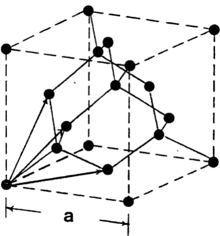
D ia m o n d is a crystal. T he m ost com m on diam ond structure has a face-centered
c ubic (fee) lattice w ith tw o c a rb o n atom s p e r p rim itiv e unit. E a c h carb o n atom
c o m b in e s its fo u r sp'^ valence e lectrons with one sp^ valence electron of four other
c a rb o n a to m s p la c e d s y m m e tric a lly a ro u n d it. This results in strong, directional,
covalent bonds called sigm a (cr) bonds [2]. T he bond length is 0.154 nm [2] while the
cubic edge is a = 3.567 Â at 0 °C [3]. D ia m o n d has the highest atom density o f any
material. This explains why diam ond is the stiffest, hardest and least com pressible of all
substances [2]. The crystal structure o f cubic diam ond is illustrated in figure II-2. Si and
Chapter II Diamond and conjugated polymers: two carbon-based electronic materials 1 6
Figure II-2 The crystal structure of cubic diamond {a is the cubic edge). (Reproduced from Ref. [3].)
In addition to the cubic symmetry of the diamond lattice there exists another important crystal structure of diamond. The carbon atoms are linked together as in the mineral wurtzite which has a hexagonal symmetry. This form of diamond was discovered in the 1960s during experiments on diamond synthesis [4]. It has also been found in meteorites [4]. This form of diamond is known as hexagonal diamond. The natural hexagonal diamond is known as lonsdaleite [2].
Chapter II Diamond and conjugated polymers: two carbon-based electronic materials 1 7
Figure II-3 Planar section of the sp^ hybrid orbitals of the carbon atom. (Reproduced from [2].)
. L
6.71
k
• C arbon atom
Figure II-4 Schematic drawing of the three dimensional structure of hexagonal graphite. (Reproduced from Ref. [2].)
Chapter II Diamond and conjugated polymers: two carbon-based electronic materials ____________ 18
are strong, covalent (T bonds of length equal to 0.141 nm [2]. The fourth free delocalised electron form a weaker van der Waals bond with another delocalised electron from an adjacent plane. This latter bond is called a pi {n) bond. The stacking of the different planes can occur in two different ways, leading to hexagonal and rhombohedral graphite. The graphite structure of hexagonal graphite (the most common form) is illustrated in figure II-4.
The sp orbital accounts for the sp bond in molecules such as the gas acetylene, HC=CH, and the carbines, (C=C)„. The sp bond is a covalent, cr, bond. The two other valence electrons of the carbon atom are free, delocalised electrons available to form 7t bonds [2].
Chapter II Diamond and conjugated polymers: two carbon-based electronic materials 19
sp
ta-C:H
H C polymers
sp u tte re d a-C
no films
g lassy C evap. C
Figure II-5 Phase diagram of diam ond-like carbon materials. (Reproduced from Ref.
[8]).
P olym ers s p 3 & s p 2
H /C >1
G raphite D iam ond
sp2 bonds
s p 3 bonds
DLC or taC
Figure II-6 D elim itation of properties o f diam o n d -lik e carb o n (R e p ro d u c e d from
Chapter II Diamond and conjugated polymers: two carbon-based electronic materials _________ 20 11.3. Dia m o n d in e l e c t r o n ic s
11.3.a. Diamond synthesis
The history of diamond synthesis has been reviewed in Refs. [4,9-11], Diamond has only become available in large quantities since it was found in alluvial deposits in South Africa near the Orange river in 1867 [4]. It was then realised that diamond could also be found by digging straight down into the earth into a rock that was not alluvial material but the vent of an extinct volcano. This indicated that natural diamond had been formed at great depth from carbonaceous material under high pressure and high temperatures conditions.
The main sources of natural diamond are nowadays located in the southern part of Africa, Siberia and Western Australia [4]. Natural diamonds can be classified within three categories: these are (i) those diamonds which can be sold as gemstones (ii) diamonds used for industrial purposes (because of their colour or the presence of defects they cannot be used as gemstones) (iii) lower quality stones, known as “boart”, used to provide grit and powder for grinding [4].
Chapter II Diamond and conjugated polymers: two carbon-based electronic materials 21 diam o n d . It m ust be n o ted (see figure II-8) that d ia m o n d is a th e r m o d y n a m ic a lly
m etastable phase o f carbon at room tem perature (RT) and under atm ospheric pressure.
How ever, the activation energy for converting diam ond back to graphite is so large that
diam ond can be considered as kinetically stable under ambient conditions [11].
50
DIAMOND
Ü
LIQ .
10
GRAPHITE
6000 4000 5000
1000 2000
Temperature (K) 3000
Figure 11-7 P ,T pha se and tra nsition d ia g ra m for c arbon. S o lid lines r e p re s e n t
e quilibrium phase boundaries. A: com m ercial synthesis o f d iam o n d from graphite by
catalysis; B: rapid solid-phase graphite to diam ond synthesis; C: fast transform ation of
d iam o n d to graphite; D: hexagonal graphite to hexagonal d iam o n d synthesis; E: shock
c om pression graphite to hexagonal d iam ond synthesis; F: shock com pression graphite
to cubic diam o n d synthesis; B, F, G: graphite or hexagonal d iam ond to cubic d iam ond
synthesis; H, I, J: com p re sse d graphite acquires diam ond-like properties, but reverts to
graphite upon release of pressure. (After Refs [1,13].)
Both synthe tic a nd natural d iam o n d s are fo rm e d u n d e r c o n d itio n s of high
pressure and high tem peratures. How ever, diam ond crystallisation can also occurs in a
te m p e ra tu re - p re s s u re reg im e w he re d ia m o n d is t h e r m o d y n a m ic a lly u n s ta b le with
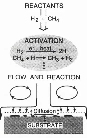
Chapter II Diamond and conjugated polymers: two carbon-based electronic materials 2 2 1373 K [11]. This can be attributed to a combination of thermodynamic, kinetic and chemical factors. The history of diamond synthesis at low pressure has been reviewed in Refs. [4,9,11]. The low-pressure synthesis of diamond was first successfully achieved by Eversole [14]. According to Angus et al. [9] Eversole’s work took place before the successful diamond synthesis by high pressure at the General Electric company, so that Eversole may have been the first to create new diamond by any method. Metastable diamond growth was also extensively studied by Derjaguin’s group in the Soviet Union from 1956 (see for instance Refs. [15-17] and references therein) as well as by Angus and co-workers at case Western Reserve University [18]. Derjaguin’s first approach consisted on the growth of diamond whiskers from a carbon containing vapour at approximately atmospheric pressure [15]. An extensive research programme at the National Institute for Research in Inorganic Materials (NIRIM) in Japan since the early 1980’s led to the development of various new techniques for the growth of diamond at low pressure. These include hot filament assisted chemical vapour deposition (HFCVD) [19,20], microwave plasma enhanced CVD (MPEGYD) [21] and radio frequency (RE) plasma CVD [22]. A schematic drawing of the MWPECVD deposition system used by Kamo et a l is shown in figure II-8.
W ave g u id e
S le e v e M a g n e tro n
I ^ Q u a r tz tu b e
S u b s tr a te
/
P lu n g e r
V acuum P um p
Chapter II Diamond and conjugated polymers: two carbon-based electronic materials 2 3 T here exists n ow adays a great variety o f m ethods to grow C V D diam ond. A
detailed review o f the different techniques can be found in Refs. [23,24]. The technique
which is c o m m o n ly used for electronic applications is M P E C V D . All of the m ethods
are b a s e d on the d iss o c iatio n o f c a r b o n - c o n ta in in g s o u rc e ga ses as well as the
generation o f atom ic hydrogen near the surface during the growth process. Hydrogen
acts as a selective etchant for rem oving graphite but not d ia m o n d during the growth
process. The process of C V D growth is illustrated in figure II-9.
REACTANTS 11
Hg + CH
4
u
A cn w iP N
CH4+H—
5 : ft
FLOW AND REACTIO N
Diffusion
SUBSTRATE
Figure II-9 A s c h em a tic sh o w in g the principal e le m e n ts in the d ia m o n d C V D
process: flow o f reactants into the reactor, activation o f the reactants by thermal and
p la s m a p rocesses, reaction and transport o f the species to the g row ing surface, and
surface chemical processes depositing diam ond and other form s o f carbon. (Reproduced
from Ref. [25].)
It is to be n o ted that, at present, the g row th o f d ia m o n d on non diam o n d
s u b s tr a te s ( h e t e r o e p i ta x y ) , su c h as silico n (Si), by C V D p r o c e s s e s leads to
Chapter II Diamond and conjugated polymers: two carbon-based electronic materials 2 4 crystal diamond (natural or synthetic diamond) is used as the substrate (homoepitaxy) material.
Il.S.b. Electronic properties of diamond
The properties of diamond as a material for electronic devices have been reviewed in [10,11,23,26,27] and are summarized in table ILL
Table II. 1 Electrical properties of diamond at RT. (From Refs. [28,29].)
Parameter Value
Bandgap Eg = 5.45 eV
Dielectric constant e = 5.7
Undoped resistivity > 10*^ Q cm
Thermal conductivity X = 2 0 W cm ' K '
Thermal expansion 1.1 X 10" K '
Electric breakdown field Ebr = 10^ V cm '
Electron saturation velocity Vg = 2.7 X 10^ cm s '
Hole saturation velocity vj = 1.0 X 10^ cm s ' Electron drift mobility [30] P e = 2400 cm^ V ' s '
Hole drift mobility [31] Ph = 2100 cm^ V ' s ' Longitudinal electron effective mass [30] niie= 1.4
Transverse electron effective mass [30] mte = 0.36
Heavy hole effective mass [31] I^hh =1. 1 Light hole effective mass [31] miij = 0.3
Diamond displays a number of attractive properties over other semiconductors for a number of electronic applications. Because of the large (indirect) bandgap* of diamond of ~ 5.5 eV the intrinsic carrier concentration at 1000 °C is comparable to that
Chapter II Diamond and conjugated polymers: two carbon-based electronic materials _________ 25 of silicon at RT. Also, the surface of diamond is stable up to 500-600 °C in air and 1400-1700 °C in inert atmosphere. For these reasons diamond has been envisaged for high temperature electronic devices. The high breakdown field (Ebr=10^ V cm'^) and the high thermal conductivity (X=20 W cm'^ K'^) are two major advantages of diamond over other semiconductors for high-frequency, high-power devices [26]. The thermal conductivity of diamond at RT is the highest of any known solid [26]. The properties of a material for electronic devices are often estimated by means of the Johnson’s [32] and Keyes’ [33] figures of merit, noted JFM and KFM, respectively. JFM is defined as:
and is usually used to compare material properties for power microwave applications. For «-type diamond JFM is roughly 90 times higher than the corresponding value for Si and is the highest among existing semiconductors [10]. The JFM is, however, slightly lower if it is estimated in the case of holes since the saturation velocity for holes is reduced by a factor of ~ 2.7 compared to that of electrons. The KFM is defined as:
KFM = A (II.3.C-2)
and is used in the case of digital integrated circuits. Here, c is the velocity of light in vacuum. Because of the high thermal conductivity of diamond, the low dielectric permittivity (e=5.7) and high saturation velocity (10^ cm s'^ for holes and 2.7 x 10^ for electrons) diamond is here as well superior to existing semiconductors.
The mobility values for diamond can differ depending on the sample considered and the technique used to measure them (i.e.. Hall mobility or drift mobility). The values given in table II I are those of pure and structurally perfect natural insulators. A comprehensive review of mobility values in diamond can be found in Ref. [29]. See also the case of boron doped diamond below.
Chapter II Diamond and conjugated polymers: two carbon-based electronic materials _________ 26 technique. From these data the hole effective mass can be evaluated from m* = ^ and the electron effective mass from m* = ) , which gives ml = 1.2m^ and m* = 0.51m^ where is the rest mass of a free electron [34]. A more comprehensive treatment of electron masses in diamond can be found in Ref. [34].
II.3.C. Defects in diamond
Defects within natural and synthetic diamond have been reviewed in Ref. [4]. The case of low-pressure CVD diamond is more specifically addressed in Ref. [27]. An ideal diamond consists of a lattice of carbon atoms as described in §11.2. and is a colourless crystal. Real diamonds contain a number of inclusions (i.e., foreign materials leading to dark spots within the crystal) as well as impurity atoms. There can also be gaps or voids between inclusions. Also, even if there are no impurities (i.e., only carbon atoms) the crystal may be imperfect with some atoms displaced from their position within the lattice. These types of defects are called geometric defects. They can be either point defects (i.e., zero-dimensional defects) such as vacancies (i.e., missing atom) and self-interstitials, or extended defects such as stacking faults (i.e., a lattice imperfection), twinning (i.e., interruption in the sequence of crystallographic planes) and dislocations (i.e., line discontinuity in the crystal lattice). In the case of CVD diamond the defect structure is even more complex [27]. For instance, varying amounts of graphitic carbon as well as impurities such as hydrogen and silicon are incorporated during the growth process. Also, CVD diamond grown on non diamond substrates is polycrystalline. Both high angle and low angle grain boundaries can form. Defects, impurities and strains tend to concentrate at grain boundaries. This is the case for instance of amorphous carbon regions as well as dopant atoms. Grain boundaries, therefore, significantly affect both the carrier transport and the thermal conductivity.
Chapter II Diamond and conjugated polymers: two carbon-based electronic materials 2 7 obtained from photoconductivity (PC) and TSC measurements are included in chapter IV and V. Additional information regarding first studies of diamond by PC may be found in Refs. [35,36].
Foreign Interstitial Atoms e.g., H, Li
Self’ Interstitial
I
Vacancy V
Foreign Substitutional Atoms e.g., N, P, B
Figure 11-10 Schematic of points defects in diamond. (Reproduced from Ref. [27].)
Chapter II Diamond and conjugated polymers: two carbon-based electronic materials _________ 28 800-1400 cm '\ and in the UV and even visible ranges. Diamonds which contain enough nitrogen (more than 1 ppm [4]) to produce a significant absorption in the range 800-1400 cm ' are known as type I diamonds; the others (about 2% of natural diamonds [4]) are known as type II diamonds. However, nitrogen in diamond can take many forms and the type I is further divided into type la and Ib. The A centre is thought to be formed of a pair of nitrogen atoms occupying substitutional sites. It gives an additional IR absorption in the range 1000-1400 cm ' as well as in the UV at energies lower than 5.5 eV. The A centre acts as a deep donor with an activation energy of ~ 4 eV below the conduction band. A second form of nitrogen-related optical centre is known as B centre. It produces a strong additional absorption in the IR range, different from the A centre, and less absorption in the UV than the A centre. A possible origin for the B centre could be an aggregate consisting of an even number of nitrogen atoms. A possible form would be four nitrogen atoms surrounding a vacancy [27]. Both A and B centres are non magnetic centres. Diamonds which contain nitrogen in the form of the A or/and B centres are known as type la. Depending on which centre makes the main contribution the type la is further divided into laA and laB. A third form of nitrogen in diamond is that of a single nitrogen atom replacing a carbon atom. This form of nitrogen also leads to additional absorption in the IR range of 1000-1500 cm ' as well as in the UV range. The absorption lines are different, however, from those produced by the A and B centres. This optical centre is paramagnetic. It is a donor with an activation energy of ~ 1.7 eV below the conduction band. When nitrogen is incorporated in diamond in this form it is known as type Ib diamond. Most of the synthetic diamonds are of type Ib. Type Ib diamonds show a yellow colour. Finally, two other forms of nitrogen in diamond not discussed above are the N3 centres and platelets. Further details about these centres can be found in Ref. [4]. The density of nitrogen in CVD diamond films is usually significantly lower than in natural or HPHT diamonds due to control of the growth environment.
Chapter II Diamond and conjugated polymers; two carbon-based electronic materials _________ 29 the presence of boron at substitutional sites. These diamonds are p-type semiconductors with an acceptor ionisation energy of 368.5 ± 1.5 meV [39]. The typical boron concentration in natural diamond is usually less than 1 ppm. Doping with boron can also easily be achieved during growth both in the case of synthetic and CVD diamonds. Synthetic diamond containing up to 1000 ppm of uncompensated boron can be produced [37]. In the case of CVD diamond incorporation of boron is usually obtained by adding diborane to the plasma gas mixture [10]. A reduction of the activation energy is observed for heavily doped films and is usually attributed to the formation of an impurity band [10]. The hole mobility in boron-doped diamond is found to decrease with increasing carrier density [10]. The hole mobility in type lib natural diamond has been measured to be in the range 700-2010 cm^ V'^ s'^ at 290 K [39]. In the case of polycrystalline CVD films typical values are in the range 1-30 cm^ V* s'^ due to carrier scattering at the grain boundaries [37] whilst values in the range 8-600 cm^ V ’ s * at RT were reported for homoépitaxial diamond layers when the carrier density was varied from 7 X 10*^ down to 7 x 10'^ cm'^ [40]. Boron doping of diamond has also been achieved by ion implantation [41-46]. The main problem here is the graphitisation of the damaged diamond regions [43,46]. In the case of CVD diamond additional problems arise during implantation from the presence of compensating impurities and defects introduced during the growth process [42]. The best results are typically achieved by implementing the procedure described by Prins known as Cold Implantation Rapid thermal Annealing (CIRA) [44-46].
Chapter II Diamond and conjugated polymers; two carbon-based electronic materials _________ 30 lithium (Li) sodium (Na) and sulfur (S) have been envisaged as «-type dopants for diamond [10,27]. The «-type character of Li, Na and S doped diamond has not been clearly demonstrated in spite of a significant research effort, especially in the case of S [50-53]. However, P doped homoépitaxial CVD layers obtained by introduction of phosphine (PH3) in the gas phase during the growth process are clearly «-type, as evidenced by Hall effect measurements [54-57]. The activation energy of the donor level was found to be at 0.43 eV in the early studies [54]. Modification of the growth process has led to an improvement of the crystal quality of P doped diamond and a shift of the activation energy of the donor level towards deeper values. A number of recent studies show that the activation energy of the ground state of P in diamond is at 0.6 eV below the CB [54-59].
Chapter II Diamond and conjugated polymers: two carbon-based electronic materials ____________ 31
suggested that it was unrelated to the blue band at 2.8 eV characteristic of natural diamond. Finally, in a recent investigation using homoépitaxial CVD films, Takeuchi et al. [64] suggested that a possible origin of the CL band A emission at 2.9 eV was sp^ defects located at dislocations or grain boundaries.
Vacancies in diamond are coupled with other defects such as impurities or grain boundaries so that their identification is not easy [27]. Vacancies have been mainly studied following irradiation using high energy electrons, gamma rays or neutrons [65-67]. The most widely studied vacancy-related features are the GR bands which can be observed both in absorption and luminescence measurements [27]. The GRl band gives absorption lines in between 1.6 and 2.4 eV with a zero phonon line at 1.673 eV[4]. Various peaks, known as GR2 to GR8 lines are also observed in between 2.8 and 3.0 eV [4]. The defect associated to the GR features is thought to be a neutral vacancy (V°) with a tetrahedral symmetry [27]. Another major vacancy-related feature is the N D l system with a zero-phonon line at 3.149 eV. This defect is thought to be due to negatively charged vacancies (V ). Other important vacancy-related features include the H3 defect related to a vacancy trapped between two nearest neighbour substitutional nitrogen atoms (N-V-N), H4 correlated to vacancies trapped at nitrogen platelet aggregates (V-B) and NV attributed to a nitrogen-vacancy pair (N-V) [27]. The incorporation o f vacancies into CVD diamond is usually higher than in natural diamond. Their concentration has been estimated to be typically of the order of 10^^ cm' ^ (10 ppm) in undoped diamond films compared to 10'* cm'^ (0.1 ppm) in natural diamond [27].
11.4. El e c t r o n ic p o l y m e r s
11.4.a. Conjugated polymers
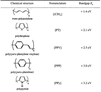
Chapter II Diamond and conjugated polymers: two carbon-based electronic materials _________ 32 common conjugated polymers is shown in table II-2. The simplest conjugated polymer is polyacetylene, which is made of a chain of repeating C-H units. Note as well the structure of PPV, one o f the most studied electroluminescent polymers. (PPV is reviewed more specifically in chapter VII.) The strong cr bonds in the backbone are responsible for the mechanical properties o f the polymer. In contrast, the unique electronic properties of conjugated polymers arise from the presence of ;r-electrons, whose wavefunctions are delocalised over long portions of the polymer chain. One of the main features of conjugated polymers is that the electronic (%-) band gap is relatively small (typically 1-3.5 eV), so that semiconducting properties are observed [68]. Furthermore, the polymer molecules can readily be oxidised or reduced (doping) leading to conducting polymers.
Table II-2 Chemical structure of a number of common conjugated polymers along with their corresponding nomenclature and banggap E^. (From Ref. [69,70].)
Chemical structure Nomenclature Bandgap Eg
= 1.4 eV
\ \ [(CH)J
/ran5-polyacetylene
polythiophene
[FT] = 2 .1 e V
poly(/?ara-phenylene vinylene)
[PPV] = 2.5 eV
poly(p<2ra-phenilene)
4 0
)
[PPP] = 3.0 eV
X [PPy] = 3.2 eV
Chapter II Diamond and conjugated polymers: two carbon-based electronic materials ____________ 3 3
Doping of conjugated polymers actually proceeds in a different way to that of an inorganic semiconductor [69]. Doping in polymers is obtained by charge injection into the macromolecular chain, usually using electrochemical reactions. The added charge is not simply a free electron or a free hole that is given to the conduction band (i.e., lowest unoccupied molecular orbital or LUMO level) or the valence band (i.e., highest occupied molecular orbital or HOMO level). In fact, the added charge interacts with the polymer chain so that a deformation of the chain is induced around the charge itself. This localised charged particule along with the deformation it creates is called a polaron. It is noted or F according to its sign. Other similar entities include bipolarons (double charged) and solitons. Solitons, noted S, can be understood as a portion of chain separating two regions of different bond alternation [71]. These quasi-particules can travel along the chain, the deformation being moved at the same time as the electron or the hole, leading to electrical conduction. For instance, the electrical conductivity in ordered thin films of iodine-doped polyacetylene is about 4 x 10^ S cm'% close to that of a single crystal of copper [68]. However, the mobility of carriers in conjugated polymers is rather low due to disorder and hopping conduction. Typical values are in the range lO "^ to 10'^ cm^ s'^ [72]. It should be noted that, in the case of electrochemical doping, the reaction can be reversed leading to the removal of the excess of carriers. Such a process is known as undoping.
II.4.b. Organic light emitting diodes
Chapter II Diamond and conjugated polymers: two carbon-based electronic materials __________ 34
excitons. W hen an exciton is form ed the electron and the hole rem ain on the same chain
b ound to each other by their electrostatic attraction and to a lesser extent by the chain
deform ation they may cause. It is to be noted, however, that exciton formation is still a
subject of debate [73].
T he simplest configuration for an O L E D is that o f a three layer device, as shown
in figure 11-13 (see also figure V I I - 1). A hole-injecting layer (anode), m ade o f a high
w ork function m aterial, is first deposited onto a transparent substrate (for instance, a
thin glass slide). T he anode itself is tra n sp a re n t so that the light p r o d u ce d in the
e m issiv e layer can escape. T ypically, in d iu m -tin -o x id e (ITO ) is used as the anode
material. T he second layer (emitter) is m ade o f the organic material. The third layer
(cathode) is an electron-injecting layer, typically m ade o f a low work function metal
such as m ag n e s iu m (Mg), calcium (Ca) or alloys such as M g :A g , L i:A g or M giln.
H o w e v er, single p o ly m e r layer devices have a n u m b e r o f d raw backs. T here is, for
instance, a strong im balance between electrons and holes, with holes often dom inating
the transport as this is the case in PPV. The most probable cause o f this is the presence
o f traps which control the transport [74]. Therefore, recom bination often takes place
n ear one of the metal contacts leading to quenching. For these reasons, bilayer devices
w here a charge (usually electron) transport layer has been added to the structure, are
preferred [72].
Emitter
W // /Æ W // // Z /
T ran sp aren t s u b stra te
Figure II-13 Simple device configuration for an O L F D .
T h e operation of an O L F D can be divided into four steps [72,74], as illustrated
in figure II-14. These are: first, carrier injection; second, carrier transport; third, carrier
Chapter II Diamond and conjugated polymers: two carbon-based electronic materials _________ 35 during the fourth step. It can be seen that during the third step electrons and holes combine to form either singlet (v) or triplet (vi) excitons (singlet excitons are produced when electrons and holes are created with opposite spins). The production of triplet excitons is detrimental to the EL efficiency because triplet excitons lead to nonradiative decay (xi). It is usually considered that triplet excitons represent 75% of the exciton population so that there is a 25% limit on EL efficiency compared with PL. For standard PPV the PL quantum efficiency is close to 30% so that a maximum internal quantum efficiency 0 ^ (i.e., number of photons emitted per electron injected) of 7% is predicted for PPV based devices [74]. It is to be noted, however, that a fraction of the singlet excitons also leads to nonradiative decay (ix) due to the presence of quenching sites such as charged excitations with deep intragap levels, chemical defects such as C=0 groups, and contaminants associated with the synthesis or processing [74]. Therefore, quenching sites further reduce the internal quantum efficiency 0 ^ of the device. As an indication, Burroughes et a l [75] measured maximum internal quantum efficiencies of only 0.05 % in the first PPV-based devices. Defect states within PPV-based devices are addressed more specifically in chapter VII.
Furthermore, it is to be noted that for practical applications, the important parameter is not the internal but rather the external quantum efficiency 0 ^ (i.e., number of photons detected per electron injected). The external quantum efficiency 0 ^ ' is obtained by multiplying 0 ^ by the fraction of photons that escape from the em issive layer. Since, in practice, only 10-20 % of the photons can escape due to internal reflection [72], 0 ^ ' is significantly lower than 0 ^ .
Chapter II Diamond and conjugated polymers: two carbon-based electronic materials 3 6
Coulom b
cap tu re C ath o d e A node
JV.
(IV)
(iii) > Exciton
Formation
(vi)
Singlet S = 0
Triplet S?»l (viii)
Exciton Decay (xi)
(ix)
G round s ta te
Figure 11-14 Schem atic diagram o f the p rocesses in volved in polym er electroluminescence; (i) hole injection and transport; (ii) electron injection and transport; (iii) electron leakage current; (iv) hole leakage current; (v) combination of electrons and holes to form singlet excitons; (vi) combination to form triplet excitons; (vii) intersystem crossing from singlet to triplet manifold; (viii) triplet-triplet annihilation to form singlet states; (ix) nonradiative decay o f singlet states via quenching sites; (x) radiative singlet emission of light; (xi) nonradiative decay of triplets to ground state. (Reproduced from [74].)
11.5. Su m m a r y
Chapter II Diamond and conjugated polymers: two carbon-based electronic materials _________ 37 significantly from those based on crystalline inorganic materials. However, as pointed out by RieB [73], the classical band theory can usually give at least a qualitative understanding of the operation of polymeric LEDs. This approach is the one which has been used in the study of trap states within PPV-based LEDs reported in chapter VII.
Re f e r e n c e s
[1] M. s . Dresselhaus and M. Endo, in Carbon Nanotubes. Synthesis, Structure, Properties and
A pplications, edited by M. S. Dresselhaus, G. Dresselhaus, and P. Avouris (Springer-Verlag,
Berlin Heidelberg, 2001), p. 11.
[2] H. O. Pierson, Hanbook o f Carbon, Graphite, Diamond and Fullerenes. Properties, Processing
and Applications (Noyes Publications, Park Ridge, New jersey, U.S.A., 1993).
[3] C. Y. Fong and B. M. Klein, in Diamond: Electronic Properties and Applications, edited by L.
S. Pan and D. R. Kania, Electronic Materials: Science and Technology (Kluwer Academic
Publishers, Boston / Dordrecht / London, 1995), p. 1.
[4] E. Wilks and J. Wilks, Properties and Applications o f Diamond (Butterworth-Heinemann Ltd,
Oxford, 1991).
[5] A. Grill, Diamond Relat. Mater. 8 ,428 (1999).
[6] Y. Lifshitz, Diamond Relat. Mater. 8,1659 (1999).
[7] S. Aisenberg and R. Chabot, J. Appl. Phys. 4 2 , 2953 (1971). [8] J. Robertson, Philos. Mag. B. 7 6 , 335 (1997).
[9] J. C. Angus and C. C. Hayman, Science 2 4 1 , 913 (1988).
[10] G. S. Gildenblat, S. A. Grot, and A. R. Badzian, Proc. IEEE 7 9 , 647 (1991). [11] W. Zhu, B. R. Stoner, B. E. Williams, and J. T. Glass, Proc. IEEE 7 9 , 621 (1991).
[12] F. P. Bundy, H. T. Hall, H. M. Strong, and R. H. Wentorf, Nature (London) 17 6 , 51 (1955). [13] F. P. Bundy, W. A. Basset, M. S. Weathers, R. J. Hemley, H. K. Mao, and A. F. Goncharov,
Carbon 34, 141 (1996).
[14] W. G. Eversole, U. S. Patent No. 3,030,187 (1962).
[15] B. V. Derjaguin, D. V. Fedoseev, V. M. Lukyanovich, B. V. Spitzin, V. A. Ryabov, and A. V.
Lavrentyev, J. Cryst. Growth 2, 380 (1968).
[16] B. V. Spitsyn, L. L. Bouilov, and B. V. Derjaguin, J. Cryst. Growth 52 , 219 (1981). [17] B. V. Spitsyn, J. Cryst. Growth 9 9 , 1162 (1990).
[18] J. C. Angus, H. A. Will, and W. S. Stanko, J. Appl. Phys. 3 9 , 2915 (1968).
Chapter II Diamond and conjugated polymers: two carbon-based electronic materials ____________ 3 8
[23] Low-Pressure Synthetic Diamond. Manufacturing and Applications, edited by B. Dischler and
C. Wild (Springer-Verlag, Berlin Heidelberg, 1998).
[24] Thin Film Diamond, edited by A. Lettington and J. W. Steeds (Chapman & Hall, London, 1994).
[25] D. G. Goodwin and J. E. Butler, in Handbook o f Industrial Diamonds and Diamond Films,
edited by M. A. Prelas, G. Popovici, and L. K. Bigelow (Marcel Dekker, Inc., New York, 1998).
[26] M. W. Geis, Proc. IEEE 7 9 , 669 (1991).
[27] W. Zhu, in Diamond: Electronic Properties and Applications, edited by L. S. Pan and D. R.
Kania, Electronic Materials: Science and Technology (Kluwer Academic Publishers, Boston /
Dordrecht / London, 1995), p. 175.
[28] D. L. Dreifus and B. A. Fox, in Handbook o f Industrial Diamonds and Diamond Films, edited
by M. A. Prelas, G. Popovici, and L. K. Bigelow (Marcel Dekker, Inc., New York, 1998).
[29] A. G. Gontar, in Handbook o f Industrial Diamonds and Diamond Films, edited by M. A. Prelas,
G. Popovici, and L. K. Bigelow (Marcel Dekker, Inc., New York, 1998).
[30] F. Nava, C. Canali, C. Jacobini, L. Reggiani, and S. F. Kozlov, Solid State Commun. 3 3 , 475 (1980).
[31] L. Reggiani, S. Bosi, C. Canali, F. Nava, and S. F. Kozlov, Solid State Commun. 3 0 , 333 (1979). [32] N. M. Johnson, RCA Rev. 2 6 , 163 (1963).
[33] R. W. Keyes, Proc. IEEE 6 3 (1975).
[34] A. T. Collins, in Handbook o f Industrial Diamonds and Diamond Films, edited by M. A. Prelas,
G. Popovici, and L. K. Bigelow (Marcel Dekker, Inc., New York, 1998).
[35] P. Denham, E. C. Lightowlers, and P. J. Dean, Phys. Rev. 1 61, 762 (1967). [36] J. A. Elmgren and D. E. Hudson, Phys. Rev. 12 8 , 1044 (1962).
[37] A. T. Collins, Ceram. Int. 2 2 , 321 (1996).
[38] R. Robertson, J. J. Fox, and A. E. Martin, Phil. Trans. Roy. Soc. (London) A 2 3 2 ,463 (1934). [39] A. T. Collins and A. W. S. Williams, J. Phys. C: Solid State 4, 1789 (1971).
[40] N. Fujimori, H. Nakahata, and T. Imai, Jpn. J. Appl. Phys. 2 9 , 824 (1990). [41] G. Braunstein and R. Kalish, J. Appl. Phys. 54, 2106 (1983).
[42] F. Fontaine, C. Uzan-Saguy, B. Philosoph, and R. Kalish, Appl. Phys. Lett. 68, 2264 (1996).
[43] R. Kalish, Diamond Relat. Mater. 2, 621 (1993).
[44] F. J. Prins, Phys. Rev. B 38, 5576 (1988). [45] F. J. Prins, Mater. Sci. Rep. 7 , 271 (1992).
[46] F. J. Prins, Nucl. Instrum. Meth. B 8 0 /8 1 , 1433 (1993). [47] H. Kawarada, Surf. Sci. Rep. 2 6 , 205 (1996).
[48] H. J. Looi, L. Y. S. Pang, A. B. Molloy, F. Jones, J. S. Foord, and R. B. Jackman, Diamond
Relat. Mater. 7, 550 (1998).
[49] H. J. Looi, L. Y. S. Pang, Y. Wang, M. D. Whitfield, and R. B. Jackman, Diamond Relat. Mater.
7, 565 (1998).
[50] M. Hasegawa, D. Takeuchi, S. Yamanaka, M. Ogura, H. Watanabe, N. Kobayashi, H. Okushi,
and K. Kajimura, Jpn. J. Appl. Phys. 38, L1519 (1999).
Chapter II Diamond and conjugated polymers: two carbon-based electronic materials ____________ 3 9
[53] I. Sakaguchi, M. N.-Gamo, Y. Kikuchi, E. Yasu, H. Haneda, T. Suzuki, and T. Ando, Phys. Rev.
B 60 (1999).
[54] S. Koizumi, M. Kamo, Y. Sato, H. Ozaki, and T. Inuzuka, Appl. Phys. Lett. 7 1 , 1065 (1997). [55] S. Koizumi, M. Kamo, Y. Sato, S. Mita, A. Sawabe, A. Reznik, C. Uzan-Saguy, and R. Kalish,
Diamond Relat. Mater. 7, 540 (1998).
[56] S. Koizumi, phys. stat. sol. (a) 172, 71 (1999).
[57] S. Koizumi, T. Teraji, and H. Kanda, Diamond Relat. Mater. 9, 935 (2000).
[58] E. Gheeraert, S. Koizumi, T. Teraji, H. Kanda, and M. Nesladek, Diamond Relat. Mater. 9, 948
(2000).
[59] M. Nesladek, K. Meykens, K. Haenen, L. M. Stals, T. Teraji, and S. Koizumi, Phys. Rev. B 5 9 ,
14 852 (1999).
[60] P. J. Dean, Phys. Rev. 13 9 , 588 (1965).
[61] H. Kawarada, Y. Yokota, Y. Mori, K. Nishimura, and A. Hiraki, J. Appl. Phys. 6 7 , 983 (1990). [62] J. Ruan, K. Kobashi, and W. J. Choyke, Appl. Phys. Lett. 60 , 3138 (1992).
[63] P. B. Klein, M. D. Crossfield, J. A. Freitas, Jr., and A. T. Collins, Phys. Rev. B 5 1 , 9634 (1995). [64] D. Takeuchi, H. Watanabe, S. Yamanaka, H. Okushi, H. Sawada, H. Ichinose, T. Sekiguchi, and
K. Kajimura, Phys. Rev. B 6 3 , 245328 (2001).
[65] R. G. Farrer and L. A. Vermeulen, J. Phys. C: Solid State 5 , 2762 (1972). [66] A. Halperin and L. A. Vermeulen, J. Phys. Chem. Solids 4 3 , 691 (1982). [67] L. A. Vermeulen and A. Halperin, J. Phys. Chem. Solids 4 5 , 771 (1984).
[68] W. R. Salaneck, S. Stafstrom, and J.-L. Brédas, Conjugated Polymer Surfaces and Interfaces
(Cambridge University Press, Cambridge, 1996).
[69] K. Potje-Kamloth, in Handbook o f Surfaces and Interfaces o f Materials, edited by H. S. Nalwa
(Academic Press, San Diego - London, 2001), p. 445.
[70] A. J. Epstein, in Organic Electronic Materials. Conjugated Polym ers and Low M olecular
Weight Organic Solids, edited by R. Farchioni and G. Grosso, Springer Series in Materials
Science (Springer-Verlag, Berlin Heidelberg, 2001), p. 3.
[71] E. M. Conwell, in Organic Electronic Materials. Conjugated Polymers and Low M olecular
Weight Organic Solids, edited by R. Farchioni and G. Grosso, Springer Series in Materials
Science (Springer-Verlag, Berlin Heidelberg, 2001), p. 127.
[72] L. J. Rothberg and A. J. Lovinger, J. Mater. Res. 11, 3174 (1996).
[73] W. RieB, in Organic Electroluminescent Materials and Devices, edited by S. Miyata and H. S.
Nalwa (Gordon and Breach Publishers, Tokyo, Ibaraki, 1997), p. 73.
[74] D. D. C. Bradley, Curr. Opin. Solid St. M. 1, 789 (1996).
[75] J. H. Burroughes, D. D. C. Bradley, A. R. Brown, R. N. Marks, K. Mackay, R. H. Friend, P. L.
Bums, and A. B. Holmes, Nature (London) 347, 539 (1990).
[76] Y. Cao, 1. D. Parker, G. Yu, C. Zhang, and A. J. Heeger, Nature (London) 3 9 7 , 414 (1999). [77] J. S. Wilson, A. S. Dhoot, A. J. A. B. Seeley, M. S. Khan, A. Kohler, and R. H. Friend, Nature
(London) 413, 828 (2001).
[78] M. Wohlgenannt, K. Tandon, S. Mazumdar, S. Ramasesha, and Z. V. Vardeny, Nature (London)
D efects within Carbon-Based Electronic Materials _____________________________________________ 4 0
C
h r p t e rI I I
E
k p e r i m e n t r l m e t h o d sIII.1 . In t r o d u c t io n
In this chapter the main techniques used are described. Additional information regarding experimental procedures more specific to a particular chapter may be found in the paragraph “Experimental Details” of that specific chapter.
III.2. Ph o t o c o n d u c t o r t h e o r y
This section describes the principles of operation of a photoconductor. The main parameters used for its characterisation are defined. This treatment has been compiled from various reports available in the literature [1-4].
The photoconductor is one of the three main types of photodetectors, the two others being the PIN diode and the avalanche photodiode. This is also probably the simplest one as it is fabricated by just placing two ohmic contacts onto a semiconductor or insulator material.* The two metal contacts may be formed at opposite ends of the material (see figure III-l) or on the top surface in a planar configuration.
Chapter III Experimental methods 4 1
IJ
r 1Figure III-l Schematic drawing showing an ideal photoconducting slab of length L with electrodes of area S equal to unity placed at opposite ends.
The dark conductivity of a semiconductor or an insulator can be expressed as:
(J = e(nfi^ + pjdp ) (in .2 -1 )
where e is the electronic charge, n and p are the thermal equilibrium densities of free electrons and holes in the dark, respectively, and and Pp are the electron and hole mobilities.* Absorption of light disturbs the free carrier densities n and p which increase by the quantities An and Ap, respectively. Assuming the material is homogeneous, i.e., n and p are uniform throughout the material, the variation of conductivity A c t which results can be written as:
Act = e ( A % + A p /c ^ ) (III.2-2)
This increase in conductivity by optical absorption is called photoconductivity. In a non homogeneous material, for instance a polycrystalline material like CVD diamond, photoconductivity can also arise from a reduction by radiation of barriers to the current flow introduced by lower conductivity regions [3].
![Table II. 1 Electrical properties of diamond at RT. (From Refs. [28,29].)](https://thumb-us.123doks.com/thumbv2/123dok_us/8391901.1385429/25.596.94.475.332.664/table-ii-electrical-properties-diamond-rt-refs.webp)
![Figure 11-10 Schematic of points defects in diamond. (Reproduced from Ref. [27].)](https://thumb-us.123doks.com/thumbv2/123dok_us/8391901.1385429/28.595.163.421.201.491/figure-schematic-points-defects-diamond-reproduced-ref.webp)