Pandian Saraswathi Yadav Engineering College, Arasanoor, Sivagangai, Tamilnadu, India
Low Power MIMO Decoding Accelerator
Using Path Decorrelator
S.David Bhaskar
1, M.Mohamed Rabiq
2PG Scholar, ECE Dept, NPR Engineering College, Dindigul, Tamil Nadu, India1 Assistant Professor, ECE Dept, NPR Engineering College, Dindigul, Tamil Nadu, India2
Abstract: This paper explains about programmable hardware accelerator that targets multiple-input-multiple-output (MIMO) decoding tasks of orthogonal frequency-division multiplexing (OFDM) systems .It delivers full programmability across different wireless standards (i.e., Wi-Fi, 3G-long term evolution, and Wi-Max) as well as different MIMO decoding algorithms with extreme energy efficiency .It delivers full programmability across different wireless standards (i.e., Wi-Fi, 3G-long term evolution, and Wi-Max). Path decorrelator is proposed for incorporating MIMO decoding accelerator for low power wireless applications.
KEYWORDS:MULTIPLE-INPUT-MULTIPLE-OUTPUT (MIMO), MULTIPLE-INPUT-MULTIPLE-OUTPUT (MIMO) DECODER, MIMO ACCELERATOR, ORTHOGONAL FREQUENCY-DIVISION MULTIPLEXING (OFDM)
I. INTRODUCTION
Pandian Saraswathi Yadav Engineering College, Arasanoor, Sivagangai, Tamilnadu, India
system subject to the need to satisfy the specifications of the standard at hand. A hardware engineer then implements the chosen algorithm with constraints on complexity, performance, and power consumption considering the parallel processing requirements for OFDM operation. This design cycle is typically repeated for every new communication standard.focus on the MIMO accelerator chip implementations.
A programmable MIMO decoder design using a software-driven processor that employs several general-purpose floating-point processing units. It is general to the extent that it is very close to a digital signal processor (DSP) requiring many processor cycles to execute a simple MIMO decoding algorithm. In addition, the design depends on the special case of using space-time block coding to simplify the matrix inversion algorithm .The MIMO accelerator is a software-programmable device that specializes in MIMO decoding, and MIMO signal processing for OFDM systems. As will be explained later, this accelerator depends on an instruction memory to store pre decoded instructions and a data memory
II. BACK GROUND AND RELATED WORKS
MIMO decoding is based on extensive matrix processing. Linear decoders (such as MMSE and ZF decoders) basically invert a channel matrix (or a variant of it). Matrix factorization [QR or singular value decomposition (SVD)] is usually applied to relax the hardware requirements for the matrix inversion. SD also requires a matrix factorization as well as several metric calculation steps that can all be reformulated into matrix form.The MIMO accelerator is a complex number vector-based processor that works on complex vector operands of length Nrxwhere Nrx is the number of receive antennas used in the MIMO system. The basic building blocks of the MIMO accelerator are shown in Fig. 1. The processing core, which is the main data path of the MIMO accelerator, specifically targets the MIMO decoding tasks. It consists of four powerful processing units that are chosen based on the minimum set of primitive operations needed to fully implement most (if not all) MIMO decoding algorithms .
Three of the four processing units are shown in Fig. 2. First is the addition unit, which is an adder/subtractor that can process two pairs of Nrx complex vectors simultaneously. Examples of its uses are the formulation of the MMSE matrix
and the calculation of the SD metrics. Second is a multiplication unit that contains four dot product blocks. Eachof which computes a single complex number that results from a dot product of two complex Nrx vectors. This allows the
multiplication unit to perform a complete vector-matrix multiplication in a single processor cycle. This multiplication unit is necessary for many MIMO decoding algorithms. Third is a reciprocal unit that computes a reciprocal of Nrx real
numbers. It is mainly used for scaling the signal power. The fourth processing unit is the rotation unit. It consists of a group of coordinate rotation (CORDIC) blocks. The rotation unit contains one super vectoring CORDIC block and Nrx
super rotation CORDIC blocks as shown in Fig. 3. A super CORDIC, whether it is a vectoring CORDIC or a rotation CORDIC, is composed of multiple simple CORDIC units that allow it to perform complex phase rotations. As all the Nrx rotation CORDIC blocks use the same rotation phases, it is only logical to use a single phase processing unit and
feed its output to the rotation CORDICs. A phase processing unit transforms a real phase value to a rotation vector that controls the individual rotation steps of a simple rotation CORDIC
Pandian Saraswathi Yadav Engineering College, Arasanoor, Sivagangai, Tamilnadu, India
tor processing cores. It also covers the automatic HDL genera-tion and the parameters that impact the actual implementation. In Section III, the authors present new hardware aspects of the MIMO accelerator. Some design tradeoffs are also presented in Section III and their effect on the resulting area, throughput, and power consumption .The test setup and test procedure for the MIMO accelerator chip. Finally, the test results are presented in Section V and compared with the dedicated MIMO decoder ASIC implementations reported in the literature.The data memory is the source for all operands as well as the target for the processing core results. Each memory location contains the data for a single OFDM subchannel. This data is logically divided into a number of complex ―matrix variables‖ of size Nrx by Nrx. When an instruction is executed for a subchannel, the chunk of data associated with the
subchannel is retrieved and then delivered to the core-input switch.
As shown in Fig. 4, the core-input switch is a two level multiplexing circuit that selects and properly arranges the complex vectors needed by the processing core—whether they are row vectors, column vectors, matrix diagonals, or a combination thereof. The memory-input switch performs the same task, but in the reverse direction. It takes the outputs of the processing units and properly packages them so as to write all data associated with the given OFDM subcarrier into the appropriate memory location. The instruction word provides the programmer with complete control of the two switching circuits, thus delivering a significant amount of flexibility.The data memory is the source for all operands as well as the target for the processing core results. Each memory location contains the data for a single OFDM subchannel. This data is logically divided in to a number of complex ―matrix variables‖ of size Nrx by Nrx. When an instruction is executed for subchannel,the chunk of data associated with the subchannel is retrieved and deliverd to core-input switch. Core –input switch is a two level mux switch that selects and
FIG 2. (A)MULTIPLIER UNIT,(B) ADDER/SUBSTRACTOR UNIT, AND (C) RECIPROCAL UNIT C= COMPLEX NUMBER,R= REAL NUMBER, AND NRX=
NUMBER OF DATA STREAMS.
And The phase memory, instruction memory, and data memory blocks. As previously mentioned, the phase memory is an static RAM (SRAM) that is dedicated to the storage of the phase outputs of the vectoring CORDICs of the rotation unit. This stored phase can be reused as the input to the super rotation CORDIC blocks for future instructions.The instruction memory is used to store predecoded instructions that run on the MIMO accelerator. An instruction is a wide control word that dictates: 1) which processing unit is to be used for a given operation; 2) the required configuration for this particular unit; 3) the data memory locations for the input. A generic processor cycle consists of four stages. They
Pandian Saraswathi Yadav Engineering College, Arasanoor, Sivagangai, Tamilnadu, India
FIG 3 ROTATION UNIT FIG.4.(A)CORE-INPUT SWITCH.(B)MEMORY-INPUT SWITCH the core-input switch is a two level multiplexing circuit that selects and properly arranges the complex vectors needed by the processing core whether they are row vectors, column vectors, matrix diagonals, or a combination thereof. The memory-input switch performs the same task, but in the reverse direction.
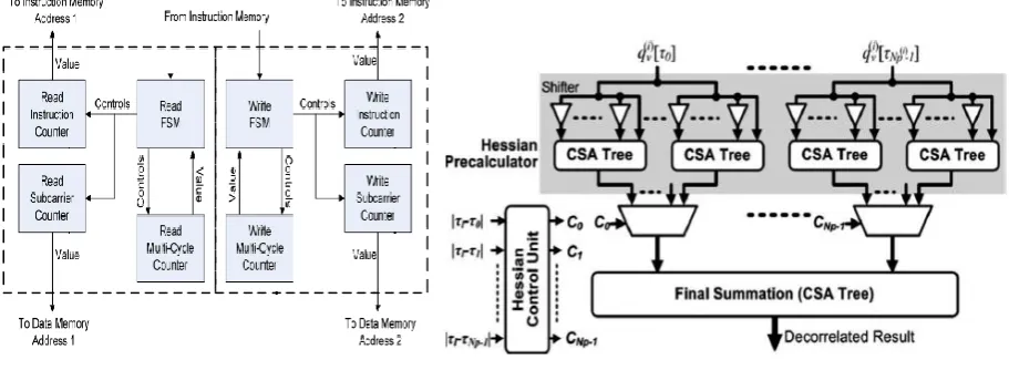
Fig 5.Block diagram of controller Fig 6.Path Decorrelator Controller
Pandian Saraswathi Yadav Engineering College, Arasanoor, Sivagangai, Tamilnadu, India
of instructions and subcarriers based on the executed instruction. It uses a subcarrier counter and an instruction counter. In general, an instruction is executed for all subcarriers of the OFDM system before a new instruction is fetched .The controller task is to control the flow of instructions and subcarriers based on the executed instruction. It uses a subcarrier counter and an instruction counter. In general, an instruction is executed for all subcarriers of the OFDM system before a new instruction is fetched. A multi cycle subprogram runs by executing all the instructions of the subprogram before incrementing the subcarrier counter to repeat this subprogram for the next subcarrier. That a single instruction is read twice whatever the mode of operation is, the controller state machine has to be run twice (simultaneously) as well. The controller hardware is thus duplicated as shown in
In Fig.5.One copy of the controller is used to manage the data read instruction and subcarrier flow, and a second copy is used to manage the data write instruction and subcarrier flow.The path decorrelator controller is used to reduce the power consumption in MIMO accelerator .The path decorrelator controller consist of level shifters, carry save adder trees, multiplexer, hessian control unit. The path decorrelator unit works based on hessian control logic. The hessian control unit generates hessian control signals based on the hessian matrix such as 3*3 unitary matrixes. The upper triangular elements in the hessian matrix are applied to the hessian logic which will generate the hessian controls. Based on this hessian controls the Path decorrelator output will be generated by applying the output of multiplexer to the Carry Save Adder unit. This relieves the accelerator and the data memory from the need for a double-frequency clock. But the top level will not be able to access the data memory during accelerator operation. This is acceptable because in a typical MIMO OFDM communication system, the outside blocks will only need to access the MIMO accelerator data memory once at the start of the packet and once at the end of the packet. No data transfer to the outside blocks is needed during the majority of the MIMO decoder operation. With this insight the complete memory read and write by the top level can be completed in Nsc clock cycles (recall that N sc is the number of subcarriers and is set to 52
for our prototype ASIC), and it is only required when a new packet is received and its channel estimates are available.
The four processing units are the most power hungry blocks in the accelerator because of the fact that they are constantly performing complex matrix operations. Following the example of a standard microcontroller architecture, we had initially connected the outputs of the core-input switch to all four processing units. This meant that for an instruction, the four units see, and effectively process, both operands even though the result of only one of the processing units is needed. This results in unnecessary dynamic power consumption in the chip. To avoid this unwanted power dissipation, additional hardware was introduced as shown in Fig 6.
To build a prototype chip for a complex system like the MIMO accelerator, a complete test plan had to be put in place. Fig. 8 shows a block diagram of the overall test setup. A Very High Speed Integrated Circuits (VHSIC) Hardware Descriptive Language (VHDL) test bench was used to generate the accelerator test vectors that included the initial contents and the expected final contents of the data memory for a given algorithm. A Virtex-4 field-programmable gate array (FPGA) was then used to transfer the memory contents to and from the accelerator. Custom software was written for the interaction between the VHDL test bench and the FPGA and a custom printed circuit board was designed and fabricated to connect the accelerator to the supply regulators, clock generator, logic analyzer probes, and the FPGA test signals An obvious problem facing the test setup was that both the data and instruction memories have wide word lengths (2048 bits and 326 bits, respectively). Such a large number of bits cannot be directly connected between the FPGA and the accelerator chip. To solve this problem, extra hardware blocks were designed and added on-chip for the sole purpose of testing the chi. The memory-input serializer works as a serial-to-parallel converter from the FPGA side to the accelerator. The memory-output serializer does the same job in the other direction. On one side, the two serializers are connected to the accelerator through the top-level ports. On the other side, they are connected to the FPGA by two 8-bits data busses.
Pandian Saraswathi Yadav Engineering College, Arasanoor, Sivagangai, Tamilnadu, India
for power measurements.
IV RESULTS AND DISCUSSION
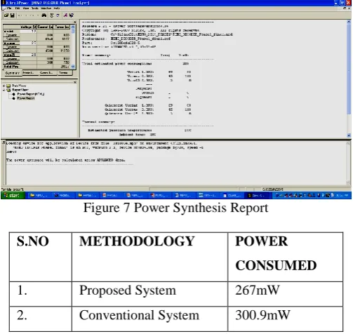
The synthesis result shown in figure .7 describes the power consumption of conventional systemMODELSIM simulation tool was developed by Mentor Graphics, Inc.., VHDL is the VHSIC Hardware Description Language. VHSIC is an abbreviation for very High Speed Integrated Circuit. It can describe the behavior and structure of electronic systems, but is particularly suited as a language to describe the structure and behavior of digital electronic designs, such as ASICs and FPGAs as well as conventional digital circuits. VHDL is a notation, and is precisely and completely defined by them Language Reference Manual (LRM). This sets VHDL apart from other hardware description e extent defined in an ad hoc way by the behavior of tools that use them. VHDL is an international standard, regulated by the IEEE. The definition of the language is non-proprietary.
VHDL is not an information model, a database scheme, a simulator, a toolset or a methodology However, a methodology and a toolset are essential for the effective use of VHDL. Simulation and synthesis are the two main kinds
Figure 7 Power Synthesis Report
S.NO METHODOLOGY POWER
CONSUMED
1. Proposed System 267mW 2. Conventional System 300.9mW
Table 1 Performance Analysis
The table 1 represents performance analysis of proposed system and conventional system. The power consumption of proposed system consumed power up to 267mW and the power consumption of conventional system consumed power up to 300.9mW
V.CONCLUSION
Pandian Saraswathi Yadav Engineering College, Arasanoor, Sivagangai, Tamilnadu, India
REFERENCES
[1] M.Shabany, D. Patel, and P. G. Gulak, ―A low-latency low-power QR-decomposition ASIC implementation in 0.13 µm CMOS,‖ IEEE Trans.Circuits Syst. I, Reg. Papers, vol. 60, no. 2, pp. 327–340, Feb. 2013.
[2] Z.-Y. Huang and P.-Y. Tsai, ―Efficient implementation of QR decompo-sition for gigabit MIMO-OFDM systems,‖ IEEE Trans. Circuits Syst. I,Reg. Papers, vol. 58, no. 10, pp. 2531–2542, Oct. 2011.
[3] K. Mohammed, M. I. A. Mohamed, and B. Daneshrad, ―A parameterized programmable MIMO decoding architecture with a scalable instruction set and compiler‖, IEEE Trans. Very Large Scale Integr. (VLSI) Syst., vol. 19, no. 8, pp. 1485–1489, Aug. 2011.4
[4] Karim Mohammed,‖ A Parameterized Programmable MIMO Decoding Architecture With a Scalable Instruction Set and Compiler‖, IEEE TRANSACTIONS ON VERY LARGE SCALE INTEGRATION (VLSI) SYSTEMS, VOL. 18, NO. 11, NOVEMBER 2010.
[5]M. Li, R. Fasthuber, D. Novo, B. Bougard, L. Van Der Perre, andF. Catthoor, ―Algorithm-architecture co-design of soft-output ML MIMO detector for parallel application specific instruction set processors‖, in Proc. DATE, Apr. 2009, pp. 1608–1613.
[7] H. S. Kim, W. Zhu, J. Bhatia, K. Mohammed, A. Shah, and B. Daneshrad, ―A practical, hardware friendly MMSE detector for MIMO-OFDM based systems‖,EURASIP J. Adv. Signal Process.,vol. 2008, p. 94, Jan. 2008.
[8] Andreas Burg,‖ VLSI Implementation of MIMO Detection Using theSphere Decoding Algorithm‖, IEEE JOURNAL OF SOLID-STATE CIRCUITS, VOL. 40, NO. 7, JULY 2005.
[9] P. Luethi, C. Studer, S. Duetsch, E. Zgraggen, H. Kaeslin,ImplementatioNand comparison‖, in Proc. IEEE APCCAS, Dec. 2008, pp. 830–833. [10] M. Karkooti, J. R. Cavallaro, and C. Dick, ―FPGA implementation ofmatrix inversion using QRD-RLS algorithm‖,in Proc. Conf. Rec. 49thAsilomar Conf. Signals, Syst. Comput., Nov. 2005, pp. 1625–1629
[11] A. J. Paulraj, D. A. Gore, R. U. Nabar, and H. Bolcskei, ―An overview of MIMO communications—A key to gigabit wireless,‖ Proc. IEEE, vol. 92, no. 2, pp. 198–218, Feb. 2004.
[12] IEEE Standard for Information Technology–Local and metropolitan Area Networks–Specific Requirements—Part 11: Wireless LAN Medium Access Control (MAC)and Physical Layer (PHY) Specifications Amendment 5: Enhancements for Higher Throughput, IEEE Standard 802.11n- 2009, Oct. 2009.
[13] IEEE Standard for Local and Metropolitan Area Networks Part 16: Air Interface for Broadband Wireless Access Systems Amendment 3: Advanced Air Interface, IEEE Standard 802.16m-2011, May 2011.
[14] M. Baker. (2009, Mar.). E-UTRA LTE Physical Layer General Description [Online].Available: http://www.in2eps.com/3g36/tk-3gpp- 36-201.html
[15] M. Baker, ―LTE-advanced physical layer,‖ in Proc. IMT Ad. Evaluation Workshop, Dec. 2009, pp. 1–48.